The future of lithography and its impact on design
|
|
|
- Ferdinand Carpenter
- 6 years ago
- Views:
Transcription


1 The future of lithography and its impact on design Chris Mack 1


2 Outline History Lessons Moore s Law Dennard Scaling Cost Trends Is Moore s Law Over? Litho scaling? The Design Gap The Future is Here 2

3 1965: Moore s Observation Components per chip Doubling each year 65,000 transistors 64 transistors! Year G. E. Moore, Cramming More Components onto Integrated Circuits, Electronics Vol. 38, No. 8 (Apr. 19, 1965) pp


4 Moore s Law Doubling every 1 2 years 25 nm Components per chip feature size + die size 25 µm Today only lithography contributes feature size + die size + device cleverness Year 4

5 Dennard s MOSFET Scaling Rules Robert Dennard Device/Circuit Parameter Scaling Factor Device dimension/thickness 1/λ Doping Concentration λ Voltage 1/λ Current 1/λ Capacitance 1/λ Delay time 1/λ Transistor power 1/λ 2 Power density 1 There are no trade-offs. Everything gets better when you shrink a transistor! 5
6 The Golden Age Dennard Scaling - as transistor shrinks it gets: Faster Lower power (constant power density) Smaller/lighter Moore s Law More transistors/chip & cost of transistor = 15%/year More powerful chip for same price Same chip for lower price Many new applications large increase in volume 6
7 Problems with Dennard Scaling Voltage stopped shrinking 10 years ago Thermal noise (kt/q = 25 mv at room temperature) Subthreshhold leakage current Gate oxide can only get so thin Interconnect dominates delay Power is at a wall Transistor variability grows with smaller size Small number of dopants per transistor, LER Today, shrinking a transistor makes it worse 7
8 Dennard + Moore Today The only benefits of shrinking a transistor today are lower cost/function and more functions/chip Moore s Law cost: despite rising fab, equipment and material costs, and increasing process complexity, the cost/cm 2 of finished silicon has remained about constant over the years. How? increasing yields increasing equipment productivity increasing wafer sizes 8
9 Chip Yield Trend 1970s High volume yields of 20 40% 1980s High volume yields of 40 60% 1990s High volume yields of 70 90% 2000s Yields must stay high, even as the technology gets more difficult (very hard to do!!) Chris Mack 9
10 Lithography Costs (single patterning) Chris Mack Wafer diameter (mm) Tool throughput (wph) Area throughput (cm^2/sec) Tool cost (M$) Tool cost ( /cm^2) 1979 g-line stepper 2004 ArF scanner 2012 ArF scanner (Note: this scaling requires that demand for chips increase by 100X) (Assumes 5-year straight line depreciation, maintenance not included) 10

11 Wafer Size Trend Time between wafer size increases is growing: Year* Wafer Diameter inch inch ,6 inch mm mm Chris Mack *first year of major production 11
12 Wafer Size and Litho Costs Litho costs scale with area, not wafers Increasing wafer size means litho costs increase as a fraction of total costs Chris Mack 150 mm wafer 25% Litho Cost 200 mm wafer 33% Litho Cost 300 mm wafer 50% Litho Cost 12
13 Litho Costs are Rising Wafer costs are very sensitive to litho costs Today, resolution improvements come ONLY from multiple patterning Litho costs must rise with multiple patterning Moore s Law costs scaling is no longer -15%/yr What is the smallest cost/transistor improvement that makes the next node worth while? 13

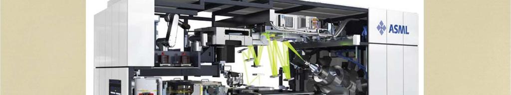
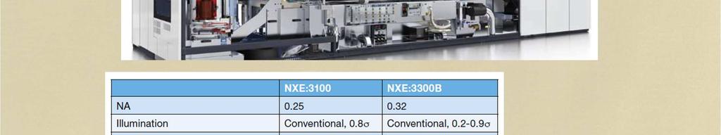
14 EUV Lithography Currently 10 wph 14
15 EUV Lithography: the Future is Not Bright Three major roadblocks to EUVL production Defect free masks (yield) High brightness source (throughput) Low line-edge roughness (LER) Current schedule calls for NXE:3300 shipping this year, going into production next year at 70 wph This will not happen In the end, it is the economics of production with EUVL that will determine its fate 15
16 The End of Litho Scaling? The reason to scale feature size is to lower the cost per transistor But if litho costs continue to rise, this benefit will likely disappear If higher litho costs mean higher cost per transistor, why reduce feature size? But wait! What about Moore s Law? 16
17 Intel s Moore s Law 10,000,000,000 1,000,000, ,000,000 10,000, Pentium 1,000, ,000 10,000 Doubling every 2.1 years 1,000 1/1/1970 1/1/1980 1/1/1990 1/1/2000 1/1/2010 1/1/
18 Intel s Moore s Law Itanium 2 10,000,000,000 1,000,000, ,000,000 10,000, Pentium 1,000, ,000 10,000 Doubling every 2.1 years 1,000 1/1/1970 1/1/1980 1/1/1990 1/1/2000 1/1/2010 1/1/


19 Intel s Itanium 2 Introduced Feb First Intel chip with 2 billion transistors 30MB Cache (1.4 billion transistors) 19
20 Intel s Moore s Law 10,000,000,000 1,000,000, ,000,000 10,000,000 1,000, Pentium Itanium 2 w/o cache 100,000 10,000 1,000 1/1/1970 1/1/1980 1/1/1990 1/1/2000 1/1/2010 1/1/
21 The Design Gap Today, we can make more transistors than we can use in logic circuits The trend in microprocessors is multiple processors per chip with lots of cache and SOC Typical chip die size is far smaller than maximum For logic, the only reason to shrink today is cost We are simply not using more transistors Flash memory has no problem using as many transistors as we can make so long as the cost per transistor keeps dropping 21
22 The Design Gap Design Gap = # transistors/chip I can make # transistors/chip I can design 22


23 Design Gap Intel Ivy Bridge 22-nm process 1.4 billion transistors Shrink from 32-nm Sandy Bridge 8.14 mm 19.5 mm 23

24 Design Gap Maximum Lithography Field Size 26 mm 33 mm 24
25 Device Cleverness How to reduce the area per transistor Isolation: LOCOS STI (shallow trench isolation) Interconnect: Single metal (all tracks between transistors) Multilevel metal (most tracks above transistors). Has this shrunk area/transistor? Transistor: Planar FinFET (gate width into the third dimension) DRAM: Folded bit line (8F 2 ) Diagonal bit line (6F 2 ) Flash: Single level cell Multilevel cell 25
26 Intel Microprocessor Device Cleverness Area/transistor/F SRAM 0 1/1/1970 1/1/1980 1/1/1990 1/1/2000 1/1/2010 1/1/2020 Introduction Date 26
27 The Future: Standard Scenario Begin using EUV lithography in 2014 Many technical hurdles May never be cost-effective: the SST of lithography? Wafer size increases to 450 mm in Lowers the cost per chip, but only for high-volume manufacturers No one knows how to pay for the equipment development costs Litho cost becomes 70 80% of chip cost Chip production is dominated by three or four super-fabs One fab costs > US$10B Moore s Law goes on as before We all have a super computer in our pocket Chris Mack 27
28 The Future: Possible Scenario 193i + DSA Very tight (single) pitch unidirectional lines cover the chip Cuts made with 193i + DSA with simple design rules Strict layout paradigm All devices are on a grid Layout choice: where to remove a line There will be no shrink of standard cell IP Every IP block must be redesigned Materials challenges High resistance lines and high resistance contacts Chris Mack 28
29 The Future: Likely Scenario Moore s Law continues only by redefining it True Moore s Law ends on Wednesday, Feb. 26, 2014 Litho is good at printing small lines/spaces, but not irregular patterns The end of shrinks Lithography still a key technology, but value moves to materials, devices, and designs The design gap is now about for logic Chris Mack 29
30 Conclusions There is Hope! The Golden Days of Moore + Dennard are over The beginning of the end of litho scaling is here Chip cost is extremely sensitive to lithography costs, and lithography costs are rising Physical limits are stochastic (line-edge roughness), but economic limits will get us first But there is hope! There is lots of room for device cleverness Fill in the design gap! 30
Advanced Digital Integrated Circuits. Lecture 2: Scaling Trends. Announcements. No office hour next Monday. Extra office hour Tuesday 2-3pm
 EE241 - Spring 20 Advanced Digital Integrated Circuits Lecture 2: Scaling Trends and Features of Modern Technologies Announcements No office hour next Monday Extra office hour Tuesday 2-3pm 2 1 Outline
Intel's 65 nm Logic Technology Demonstrated on 0.57 µm 2 SRAM Cells
 Intel's 65 nm Logic Technology Demonstrated on 0.57 µm 2 SRAM Cells Mark Bohr Intel Senior Fellow Director of Process Architecture & Integration Intel 1 What are We Announcing? Intel has fabricated fully-functional
Lecture #29. Moore s Law
 Lecture #29 ANNOUNCEMENTS HW#15 will be for extra credit Quiz #6 (Thursday 5/8) will include MOSFET C-V No late Projects will be accepted after Thursday 5/8 The last Coffee Hour will be held this Thursday
EE241 - Spring 2013 Advanced Digital Integrated Circuits. Announcements. Sign up for Piazza if you haven t already
 EE241 - Spring 2013 Advanced Digital Integrated Circuits Lecture 2: Scaling Trends and Features of Modern Technologies Announcements Sign up for Piazza if you haven t already 2 1 Assigned Reading R.H.
Trends and Challenges in VLSI Technology Scaling Towards 100nm
 Trends and Challenges in VLSI Technology Scaling Towards 100nm Stefan Rusu Intel Corporation stefan.rusu@intel.com September 2001 Stefan Rusu 9/2001 2001 Intel Corp. Page 1 Agenda VLSI Technology Trends
Transistor Scaling in the Innovation Era. Mark Bohr Intel Senior Fellow Logic Technology Development August 15, 2011
 Transistor Scaling in the Innovation Era Mark Bohr Intel Senior Fellow Logic Technology Development August 15, 2011 MOSFET Scaling Device or Circuit Parameter Scaling Factor Device dimension tox, L, W
TWINSCAN XT:1950i Water-based immersion taken to the max Enabling fast, single-exposure lithography at sub 40 nm
 TWINSCAN XT:1950i Water-based immersion taken to the max Enabling fast, single-exposure lithography at sub 40 nm SEMICON West, San Francisco July 14-18, 2008 Slide 1 The immersion pool becomes an ocean
Multiple Patterning for Immersion Extension and EUV Insertion. Chris Bencher Distinguished Member of Technical Staff Applied Materials CTO group
 Multiple Patterning for Immersion Extension and EUV Insertion Chris Bencher Distinguished Member of Technical Staff Applied Materials CTO group Abstract Multiple Patterning for Immersion Extension and
FinFET vs. FD-SOI Key Advantages & Disadvantages
 FinFET vs. FD-SOI Key Advantages & Disadvantages Amiad Conley Technical Marketing Manager Process Diagnostics & Control, Applied Materials ChipEx-2014, Apr 2014 1 Moore s Law The number of transistors
CS4617 Computer Architecture
 1/26 CS4617 Computer Architecture Lecture 2 Dr J Vaughan September 10, 2014 2/26 Amdahl s Law Speedup = Execution time for entire task without using enhancement Execution time for entire task using enhancement
VLSI: An Introduction
 Chapter 1 UEEA2223/UEEG4223 Integrated Circuit Design VLSI: An Introduction Prepared by Dr. Lim Soo King 02 Jan 2011. Chapter 1 VLSI Design: An Introduction... 1 1.0 Introduction... 1 1.0.1 Early Computing
NANOELECTRONIC TECHNOLOGY: CHALLENGES IN THE 21st CENTURY
 NANOELECTRONIC TECHNOLOGY: CHALLENGES IN THE 21st CENTURY S. M. SZE National Chiao Tung University Hsinchu, Taiwan And Stanford University Stanford, California ELECTRONIC AND SEMICONDUCTOR INDUSTRIES
Manufacturing Case Studies: Copy Exactly (CE!) and the two-year cycle at Intel
 and the two-year cycle at Intel") Manufacturing Case Studies: Copy Exactly (CE!) and the two-year cycle at Intel Paolo A. Gargini Director Technology Strategy Intel Fellow 1 Agenda 2-year cycle Copy Exactly Conclusions 2 I see no reason
Manufacturing Case Studies: Copy Exactly (CE!) and the two-year cycle at Intel Paolo A. Gargini Director Technology Strategy Intel Fellow 1 Agenda 2-year cycle Copy Exactly Conclusions 2 I see no reason
450mm and Moore s Law Advanced Packaging Challenges and the Impact of 3D
 450mm and Moore s Law Advanced Packaging Challenges and the Impact of 3D Doug Anberg VP, Technical Marketing Ultratech SOKUDO Lithography Breakfast Forum July 10, 2013 Agenda Next Generation Technology
Chapter 1, Introduction
 Introduction to Semiconductor Manufacturing Technology Chapter 1, Introduction hxiao89@hotmail.com 1 Objective After taking this course, you will able to Use common semiconductor terminology Describe a
Scaling of Semiconductor Integrated Circuits and EUV Lithography
 Scaling of Semiconductor Integrated Circuits and EUV Lithography ( 半導体集積回路の微細化と EUV リソグラフィー ) December 13, 2016 EIDEC (Emerging nano process Infrastructure Development Center, Inc.) Hidemi Ishiuchi 1 OUTLINE
Newer process technology (since 1999) includes :
 includes :") Newer process technology (since 1999) includes : copper metalization hi-k dielectrics for gate insulators si on insulator strained silicon lo-k dielectrics for interconnects Immersion lithography for masks
Newer process technology (since 1999) includes : copper metalization hi-k dielectrics for gate insulators si on insulator strained silicon lo-k dielectrics for interconnects Immersion lithography for masks
Holistic View of Lithography for Double Patterning. Skip Miller ASML
 Holistic View of Lithography for Double Patterning Skip Miller ASML Outline Lithography Requirements ASML Holistic Lithography Solutions Conclusions Slide 2 Shrink Continues Lithography keeps adding value
Introduction to VLSI ASIC Design and Technology
 Introduction to VLSI ASIC Design and Technology Paulo Moreira CERN - Geneva, Switzerland Paulo Moreira Introduction 1 Outline Introduction Is there a limit? Transistors CMOS building blocks Parasitics
ATV 2011: Computer Engineering
 ATV 2011: Technology Trends in Computer Engineering Professor Per Larsson-Edefors ATV 2011, L1, Per Larsson-Edefors Page 1 Solid-State Devices www.cse.chalmers.se/~perla/ugrad/ SemTech/Lectures_2000.pdf
PUSHING LITHOGRAPHY TO ENABLE ULTIMATE NANO-ELECTRONICS. LUC VAN DEN HOVE President & CEO imec
 PUSHING LITHOGRAPHY TO ENABLE ULTIMATE NANO-ELECTRONICS LUC VAN DEN HOVE President & CEO imec OUTLINE! Industry drivers! Roadmap extension! Lithography options! Innovation through global collaboration
Practical Information
 EE241 - Spring 2010 Advanced Digital Integrated Circuits TuTh 3:30-5pm 293 Cory Practical Information Instructor: Borivoje Nikolić 550B Cory Hall, 3-9297, bora@eecs Office hours: M 10:30am-12pm Reader:
(Complementary E-Beam Lithography)
") Extending Optical Lithography with C E B L (Complementary E-Beam Lithography) July 13, 2011 4008 Burton Drive, Santa Clara, CA 95054 Outline Complementary Lithography E-Beam Complements Optical Multibeam
Extending Optical Lithography with C E B L (Complementary E-Beam Lithography) July 13, 2011 4008 Burton Drive, Santa Clara, CA 95054 Outline Complementary Lithography E-Beam Complements Optical Multibeam
ISSCC 2003 / SESSION 1 / PLENARY / 1.1
 ISSCC 2003 / SESSION 1 / PLENARY / 1.1 1.1 No Exponential is Forever: But Forever Can Be Delayed! Gordon E. Moore Intel Corporation Over the last fifty years, the solid-state-circuits industry has grown
Practical Information
 EE241 - Spring 2013 Advanced Digital Integrated Circuits MW 2-3:30pm 540A/B Cory Practical Information Instructor: Borivoje Nikolić 509 Cory Hall, 3-9297, bora@eecs Office hours: M 11-12, W 3:30pm-4:30pm
EUVL Scanners Operational at Chipmakers. Skip Miller Semicon West 2011
 EUVL Scanners Operational at Chipmakers Skip Miller Semicon West 2011 Outline ASML s Lithography roadmap to support Moore s Law Progress on NXE:3100 (0.25NA) EUV systems Progress on NXE:3300 (0.33NA) EUV
Progress due to: Feature size reduction - 0.7X/3 years (Moore s Law). Increasing chip size - 16% per year. Creativity in implementing functions.
. Increasing chip size - 16% per year. Creativity in implementing functions.") Introduction - Chapter 1 Evolution of IC Fabrication 1960 and 1990 integrated t circuits. it Progress due to: Feature size reduction - 0.7X/3 years (Moore s Law). Increasing chip size - 16% per year. Creativity
Introduction - Chapter 1 Evolution of IC Fabrication 1960 and 1990 integrated t circuits. it Progress due to: Feature size reduction - 0.7X/3 years (Moore s Law). Increasing chip size - 16% per year. Creativity
40nm Node CMOS Platform UX8
 FUKAI Toshinori, IKEDA Masahiro, TAKAHASHI Toshifumi, NATSUME Hidetaka Abstract The UX8 is the latest process from NEC Electronics. It uses the most advanced exposure technology to achieve twice the gate
FUTURE PROSPECTS FOR CMOS ACTIVE PIXEL SENSORS
 FUTURE PROSPECTS FOR CMOS ACTIVE PIXEL SENSORS Dr. Eric R. Fossum Jet Propulsion Laboratory Dr. Philip H-S. Wong IBM Research 1995 IEEE Workshop on CCDs and Advanced Image Sensors April 21, 1995 CMOS APS
MICROPROCESSOR TECHNOLOGY
 MICROPROCESSOR TECHNOLOGY Assis. Prof. Hossam El-Din Moustafa Lecture 3 Ch.1 The Evolution of The Microprocessor 17-Feb-15 1 Chapter Objectives Introduce the microprocessor evolution from transistors to
EUVL getting ready for volume introduction
 EUVL getting ready for volume introduction SEMICON West 2010 Hans Meiling, July 14, 2010 Slide 1 public Outline ASML s Lithography roadmap to support Moore s Law Progress on 0.25NA EUV systems Progress
+1 (479)
") Introduction to VLSI Design http://csce.uark.edu +1 (479) 575-6043 yrpeng@uark.edu Invention of the Transistor Vacuum tubes ruled in first half of 20th century Large, expensive, power-hungry, unreliable
Introduction to VLSI Design http://csce.uark.edu +1 (479) 575-6043 yrpeng@uark.edu Invention of the Transistor Vacuum tubes ruled in first half of 20th century Large, expensive, power-hungry, unreliable
Homework 10 posted just for practice. Office hours next week, schedule TBD. HKN review today. Your feedback is important!
 EE141 Fall 2005 Lecture 26 Memory (Cont.) Perspectives Administrative Stuff Homework 10 posted just for practice No need to turn in Office hours next week, schedule TBD. HKN review today. Your feedback
1 Digital EE141 Integrated Circuits 2nd Introduction
 Digital Integrated Circuits Introduction 1 What is this lecture about? Introduction to digital integrated circuits + low power circuits Issues in digital design The CMOS inverter Combinational logic structures
Microprocessor Design in the Nanoscale Era
 Microprocessor Design in the Nanoscale Era Stefan Rusu Senior Principal Engineer Intel Corporation IEEE Fellow stefan.rusu@intel.com 2012 Stefan Intel Rusu Corporation July 2012 1 Agenda Microprocessor
Introduction. Digital Integrated Circuits A Design Perspective. Jan M. Rabaey Anantha Chandrakasan Borivoje Nikolic. July 30, 2002
 Digital Integrated Circuits A Design Perspective Jan M. Rabaey Anantha Chandrakasan Borivoje Nikolic Introduction July 30, 2002 1 What is this book all about? Introduction to digital integrated circuits.
EE4800 CMOS Digital IC Design & Analysis. Lecture 1 Introduction Zhuo Feng
 EE4800 CMOS Digital IC Design & Analysis Lecture 1 Introduction Zhuo Feng 1.1 Prof. Zhuo Feng Office: EERC 730 Phone: 487-3116 Email: zhuofeng@mtu.edu Class Website http://www.ece.mtu.edu/~zhuofeng/ee4800fall2010.html
Low Transistor Variability The Key to Energy Efficient ICs
 Low Transistor Variability The Key to Energy Efficient ICs 2 nd Berkeley Symposium on Energy Efficient Electronic Systems 11/3/11 Robert Rogenmoser, PhD 1 BEES_roro_G_111103 Copyright 2011 SuVolta, Inc.
Lecture Wrap up. December 13, 2005
 6.012 Microelectronic Devices and Circuits Fall 2005 Lecture 26 1 Lecture 26 6.012 Wrap up December 13, 2005 Contents: 1. 6.012 wrap up Announcements: Final exam TA review session: December 16, 7:30 9:30
Photolithography I ( Part 1 )
") 1 Photolithography I ( Part 1 ) Chapter 13 : Semiconductor Manufacturing Technology by M. Quirk & J. Serda Bjørn-Ove Fimland, Department of Electronics and Telecommunication, Norwegian University of Science
1 Photolithography I ( Part 1 ) Chapter 13 : Semiconductor Manufacturing Technology by M. Quirk & J. Serda Bjørn-Ove Fimland, Department of Electronics and Telecommunication, Norwegian University of Science
PC accounts for 353 Cory will be created early next week (when the class list is completed) Discussions & Labs start in Week 3
 Discussions & Labs start in Week 3") EE141 Fall 2005 Lecture 2 Design Metrics Admin Page Everyone should have a UNIX account on Cory! This will allow you to run HSPICE! If you do not have an account, check: http://www-inst.eecs.berkeley.edu/usr/
EE141 Fall 2005 Lecture 2 Design Metrics Admin Page Everyone should have a UNIX account on Cory! This will allow you to run HSPICE! If you do not have an account, check: http://www-inst.eecs.berkeley.edu/usr/
EECS 151/251A Spring 2019 Digital Design and Integrated Circuits. Instructors: Wawrzynek. Lecture 8 EE141
 EECS 151/251A Spring 2019 Digital Design and Integrated Circuits Instructors: Wawrzynek Lecture 8 EE141 From the Bottom Up IC processing CMOS Circuits (next lecture) EE141 2 Overview of Physical Implementations
Intel Technology Journal
 Volume 06 Issue 02 Published, May 16, 2002 ISSN 1535766X Intel Technology Journal Semiconductor Technology and Manufacturing The Intel Lithography Roadmap A compiled version of all papers from this issue
Fin-Shaped Field Effect Transistor (FinFET) Min Ku Kim 03/07/2018
 Min Ku Kim 03/07/2018") Fin-Shaped Field Effect Transistor (FinFET) Min Ku Kim 03/07/2018 ECE 658 Sp 2018 Semiconductor Materials and Device Characterizations OUTLINE Background FinFET Future Roadmap Keeping up w/ Moore s Law
Fin-Shaped Field Effect Transistor (FinFET) Min Ku Kim 03/07/2018 ECE 658 Sp 2018 Semiconductor Materials and Device Characterizations OUTLINE Background FinFET Future Roadmap Keeping up w/ Moore s Law
Semiconductor Devices
 Semiconductor Devices - 2014 Lecture Course Part of SS Module PY4P03 Dr. P. Stamenov School of Physics and CRANN, Trinity College, Dublin 2, Ireland Hilary Term, TCD 3 th of Feb 14 MOSFET Unmodified Channel
HOW TO CONTINUE COST SCALING. Hans Lebon
 HOW TO CONTINUE COST SCALING Hans Lebon OUTLINE Scaling & Scaling Challenges Imec Technology Roadmap Wafer size scaling : 450 mm 2 COST SCALING IMPROVED PERFORMANCE 3 GLOBAL TRAFFIC FORECAST Cloud Traffic
EMT 251 Introduction to IC Design
 EMT 251 Introduction to IC Design (Pengantar Rekabentuk Litar Terkamir) Semester II 2011/2012 Introduction to IC design and Transistor Fundamental Some Keywords! Very-large-scale-integration (VLSI) is
BCD Smart Power Roadmap Trends and Challenges. Giuseppe Croce NEREID WORKSHOP Smart Energy Bertinoro, October 20 th
 BCD Smart Power Roadmap Trends and Challenges Giuseppe Croce NEREID WORKSHOP Smart Energy Bertinoro, October 20 th Outline 2 Introduction Major Trends in Smart Power ASICs An insight on (some) differentiating
EE 330 Lecture 7. Design Rules. IC Fabrication Technology Part 1
 EE 330 Lecture 7 Design Rules IC Fabrication Technology Part 1 Review from Last Time Technology Files Provide Information About Process Process Flow (Fabrication Technology) Model Parameters Design Rules
Acknowledgements. o Stephen Tobin. o Jason Malik. o Dr. Dragan Djurdjanovic. o Samsung Austin Semiconductor, Machine Learning
 Semicon West 2016 Acknowledgements o Stephen Tobin o Samsung Austin Semiconductor, Machine Learning o Jason Malik o Samsung Austin Semiconductor, Metrology o Dr. Dragan Djurdjanovic o University of Texas,
450mm silicon wafers specification challenges. Mike Goldstein Intel Corp.
 450mm silicon wafers specification challenges Mike Goldstein Intel Corp. Outline Background 450mm transition program 450mm silicon evolution Mechanical grade wafers (spec case study) Developmental (test)
6.012 Microelectronic Devices and Circuits
 MIT, Spring 2009 6.012 Microelectronic Devices and Circuits Charles G. Sodini Jing Kong Shaya Famini, Stephanie Hsu, Ming Tang Lecture 1 6.012 Overview Contents: Overview of 6.012 Reading Assignment: Howe
IC Knowledge LLC, PO Box 20, Georgetown, MA Ph: (978) , Fx: (978)
 , Fx: (978)") IC Knowledge LLC, PO Box 20, Georgetown, MA 01833 www.icknowledge.com Ph: (978) 352 7610, Fx: (978) 352 3870 Linx Consulting, PO Box 384, Mendon, MA 01756 0384 www.linxconsulting.com Ph: (617) 273 8837
IC Knowledge LLC, PO Box 20, Georgetown, MA 01833 www.icknowledge.com Ph: (978) 352 7610, Fx: (978) 352 3870 Linx Consulting, PO Box 384, Mendon, MA 01756 0384 www.linxconsulting.com Ph: (617) 273 8837
45nm Foundry CMOS with Mask-Lite Reduced Mask Costs
 This work is sponsored in part by the Air Force Research Laboratory (AFRL/RVSE) 45nm Foundry CMOS with Mask-Lite Reduced Mask Costs 21 March 2012 This work is sponsored in part by the National Aeronautics
Intel Demonstrates High-k + Metal Gate Transistor Breakthrough on 45 nm Microprocessors
 Intel Demonstrates High-k + Metal Gate Transistor Breakthrough on 45 nm Microprocessors Mark Bohr Intel Senior Fellow Logic Technology Development Kaizad Mistry 45 nm Program Manager Logic Technology Development
CMOS Technology & Business Trends
 CMOS Technology & Business Trends Can the semiconductor industry afford to continue advancing? Peter M. O Neill Automated Test Innovations Agilent Laboratories Disclaimers Not a thoroughly researched paper
32nm High-K/Metal Gate Version Including 2nd Generation Intel Core processor family
 From Sand to Silicon Making of a Chip Illustrations 32nm High-K/Metal Gate Version Including 2nd Generation Intel Core processor family April 2011 1 The illustrations on the following foils are low resolution
CMOS Digital Integrated Circuits Lec 2 Fabrication of MOSFETs
 CMOS Digital Integrated Circuits Lec 2 Fabrication of MOSFETs 1 CMOS Digital Integrated Circuits 3 rd Edition Categories of Materials Materials can be categorized into three main groups regarding their
UV Nanoimprint Stepper Technology: Status and Roadmap. S.V. Sreenivasan Sematech Litho Forum May 14 th, 2008
 UV Nanoimprint Stepper Technology: Status and Roadmap S.V. Sreenivasan Sematech Litho Forum May 14 th, 2008 Overview Introduction Stepper technology status: Patterning and CD Control Through Etch Alignment
Nanometer Technologies: Where Design and Manufacturing Converge. Walden C. Rhines CHAIRMAN & CEO
 Nanometer Technologies: Where Design and Manufacturing Converge Walden C. Rhines CHAIRMAN & CEO Nanometer Technologies: Where Design and Manufacturing Converge Nanometer technologies make designers aware
EUV Supporting Moore s Law
 EUV Supporting Moore s Law Marcel Kemp Director Investor Relations - Europe DB 2014 TMT Conference London September 4, 2014 Forward looking statements This document contains statements relating to certain
EUV lithography: today and tomorrow
 EUV lithography: today and tomorrow Vadim Banine, Stuart Young, Roel Moors Dublin, October 2012 Resolution/half pitch, "Shrink" [nm] EUV DPT ArFi ArF KrF Industry roadmap towards < 10 nm resolution Lithography
Present Status and Future Prospects of EUV Lithography
 3rd EUV-FEL Workshop Present Status and Future Prospects of EUV Lithography (EUV リソグラフィーの現状と将来展望 ) December 11, 2011 Evolving nano process Infrastructure Development Center, Inc. (EIDEC) Hidemi Ishiuchi
18nm FinFET. Lecture 30. Perspectives. Administrivia. Power Density. Power will be a problem. Transistor Count
 18nm FinFET Double-gate structure + raised source/drain Lecture 30 Perspectives Gate Silicon Fin Source BOX Gate X. Huang, et al, 1999 IEDM, p.67~70 Drain Si fin - Body! I d [ua/um] 400-1.50 V 350 300-1.25
Leading at the edge TECHNOLOGY AND MANUFACTURING DAY
 Leading at the edge 22FFL technology MARK BOHR Intel Senior Fellow, Technology and Manufacturing Group Director, Process Architecture and Integration Disclosures Intel Technology and Manufacturing Day
Enabling Breakthroughs In Technology
 Enabling Breakthroughs In Technology Mike Mayberry Director of Components Research VP, Technology and Manufacturing Group Intel Corporation June 2011 Defined To be defined Enabling a Steady Technology
Digital Integrated Circuits Perspectives. Administrivia
 Lecture 30 Perspectives Administrivia Final on Friday December 14, 2001 8 am Location: 180 Tan Hall Topics all what was covered in class. Review Session - TBA Lab and hw scores to be posted on the web
The Transistor. Survey: What is Moore s Law? Survey: What is Moore s Law? Technology Unit Overview. Technology Generations
 CSE 560 Computer Systems Architecture Technology Survey: What is Moore s Law? What does Moore s Law state? A. The length of a transistor halves every 2 years. B. The number of transistors on a chip will
Chapter 15 Summary and Future Trends
 Chapter 15 Summary and Future Trends Hong Xiao, Ph. D. hxiao89@hotmail.com www2.austin.cc.tx.us/hongxiao/book.htm Hong Xiao, Ph. D. www2.austin.cc.tx.us/hongxiao/book.htm 1 The 1960s First IC product Bipolar
Lecture 0: Introduction
 Lecture 0: Introduction Introduction Integrated circuits: many transistors on one chip. Very Large Scale Integration (VLSI): bucketloads! Complementary Metal Oxide Semiconductor Fast, cheap, low power
FinFET-based Design for Robust Nanoscale SRAM
 FinFET-based Design for Robust Nanoscale SRAM Prof. Tsu-Jae King Liu Dept. of Electrical Engineering and Computer Sciences University of California at Berkeley Acknowledgements Prof. Bora Nikoli Zheng
Sub-micron technology IC fabrication process trends SOI technology. Development of CMOS technology. Technology problems due to scaling
 Goodbye Microelectronics Welcome Nanoelectronics Sub-micron technology IC fabrication process trends SOI technology SiGe Tranzistor in 50nm process Virus The thickness of gate oxide= 1.2 nm!!! Today we
Reducing Transistor Variability For High Performance Low Power Chips
 Reducing Transistor Variability For High Performance Low Power Chips HOT Chips 24 Dr Robert Rogenmoser Senior Vice President Product Development & Engineering 1 HotChips 2012 Copyright 2011 SuVolta, Inc.
The 28 nm CMOS Power Amplifier
 The 28 nm CMOS Power Amplifier IECC 2017 Keynote talk 2017-05-19 Ted Johansson, Integrated Circuits and System, Dept. of Electrical Engineering, Linköping University, Sweden ted.johansson@liu.se Outline
EE5324. VLSI Design II
 EE5324 VLSI Design II Professor Chris H. Kim University of Minnesota Dept. of ECE www.umn.edu/~chriskim/ chriskim@umn.edu Practical Information Class webpage http://www.ece.umn.edu/class/ee5324 Instructor:
Semiconductor Memory: DRAM and SRAM. Department of Electrical and Computer Engineering, National University of Singapore
 Semiconductor Memory: DRAM and SRAM Outline Introduction Random Access Memory (RAM) DRAM SRAM Non-volatile memory UV EPROM EEPROM Flash memory SONOS memory QD memory Introduction Slow memories Magnetic
Innovation to Advance Moore s Law Requires Core Technology Revolution
 Innovation to Advance Moore s Law Requires Core Technology Revolution Klaus Schuegraf, Ph.D. Chief Technology Officer Silicon Systems Group Applied Materials UC Berkeley Seminar March 9 th, 2012 Innovation
Toward 5nm node ; Untoward Scaling with Multi-patterning
 1 st International Symposium on DSA Toward 5nm node ; Untoward Scaling with Multi-patterning 27 th OCT 2015 H. Yaegashi Chief Engineer Tokyo Electron Limited Down-caling trend towards N5 N20 N14 N10 N7
1. Introduction. Institute of Microelectronic Systems. Status of Microelectronics Technology. (nm) Core voltage (V) Gate oxide thickness t OX
 Core voltage (V) Gate oxide thickness t OX") Threshold voltage Vt (V) and power supply (V) 1. Introduction Status of s Technology 10 5 2 1 0.5 0.2 0.1 V dd V t t OX 50 20 10 5 2 Gate oxide thickness t OX (nm) Future VLSI chip 2005 2011 CMOS feature
Threshold voltage Vt (V) and power supply (V) 1. Introduction Status of s Technology 10 5 2 1 0.5 0.2 0.1 V dd V t t OX 50 20 10 5 2 Gate oxide thickness t OX (nm) Future VLSI chip 2005 2011 CMOS feature
ECE 5745 Complex Digital ASIC Design Topic 2: CMOS Devices
 ECE 5745 Complex Digital ASIC Design Topic 2: CMOS Devices Christopher Batten School of Electrical and Computer Engineering Cornell University http://www.csl.cornell.edu/courses/ece5950 Simple Transistor
CMOS Technology. 1. Why CMOS 2. Qualitative MOSFET model 3. Building a MOSFET 4. CMOS logic gates. Handouts: Lecture Slides. metal ndiff.
 CMOS Technology 1. Why CMOS 2. Qualitative MOSFET model 3. Building a MOSFET 4. CMOS logic gates poly pdiff metal ndiff Handouts: Lecture Slides L03 - CMOS Technology 1 Building Bits from Atoms V in V
Used Semiconductor Manufacturing Equipment: Looking for Sales in All the Right Places. Study Number MA108-09
 Study Number MA108-09 August 2009 Copyright Semico Research, 2009. All rights reserved. Reproduction in whole or part is prohibited without permission of Semico. The contents of this report represent
Spring of EUVL: SPIE 2012 AL EUVL Conference Review
 Spring of EUVL: SPIE 2012 AL EUVL Conference Review Vivek Bakshi, EUV Litho, Inc., Austin, Texas Monday, February 20, 2012 The SPIE Advanced Lithography EUVL Conference is usually held close to spring,
Session 3: Solid State Devices. Silicon on Insulator
 Session 3: Solid State Devices Silicon on Insulator 1 Outline A B C D E F G H I J 2 Outline Ref: Taurand Ning 3 SOI Technology SOl materials: SIMOX, BESOl, and Smart Cut SIMOX : Synthesis by IMplanted
LSI ON GLASS SUBSTRATES
 LSI ON GLASS SUBSTRATES OUTLINE Introduction: Why System on Glass? MOSFET Technology Low-Temperature Poly-Si TFT Technology System-on-Glass Technology Issues Conclusion System on Glass CPU SRAM DRAM EEPROM
Copyright 2003 by the Society of Photo-Optical Instrumentation Engineers.
 Copyright 2003 by the Society of Photo-Optical Instrumentation Engineers. This paper was published in the proceedings of Optical Microlithography XVI, SPIE Vol. 5040, pp. xxi-xxxi. It is made available
Jan M. Rabaey Anantha Chandrakasan Borivoje Nikolic. July 30, Digital EE141 Integrated Circuits 2nd Introduction
 Digital Integrated Circuits A Design Perspective Jan M. Rabaey Anantha Chandrakasan Borivoje Nikolic Introduction July 30, 2002 1 What is this book all about? Introduction to digital integrated circuits.
Chapter 3 Basics Semiconductor Devices and Processing
 Chapter 3 Basics Semiconductor Devices and Processing 1 Objectives Identify at least two semiconductor materials from the periodic table of elements List n-type and p-type dopants Describe a diode and
Kenneth R. Laker, University of Pennsylvania, updated 20Jan15
 http://www.seas.upenn.edu/~ese570/ 1 TOPICS The Course Industry Trends Digital CMOS Basics Some VLSI Fundamentals Illustrative Design Example 2 1. Apply principles of hierarchical digital CMOS VLSI, from
Low-Power VLSI. Seong-Ook Jung VLSI SYSTEM LAB, YONSEI University School of Electrical & Electronic Engineering
 Low-Power VLSI Seong-Ook Jung 2013. 5. 27. sjung@yonsei.ac.kr VLSI SYSTEM LAB, YONSEI University School of Electrical & Electronic Engineering Contents 1. Introduction 2. Power classification & Power performance
Chapter 3: Basics Semiconductor Devices and Processing 2006/9/27 1. Topics
 Chapter 3: Basics Semiconductor Devices and Processing 2006/9/27 1 Topics What is semiconductor Basic semiconductor devices Basics of IC processing CMOS technologies 2006/9/27 2 1 What is Semiconductor
Contribution of Gate Induced Drain Leakage to Overall Leakage and Yield Loss in Digital submicron VLSI Circuits
 Contribution of Gate Induced Drain Leakage to Overall Leakage and Yield Loss in Digital submicron VLSI Circuits Oleg Semenov, Andrzej Pradzynski * and Manoj Sachdev Dept. of Electrical and Computer Engineering,
From Sand to Silicon Making of a Chip Illustrations May 2009
 From Sand to Silicon Making of a Chip Illustrations May 2009 1 The illustrations on the following foils are low resolution images that visually support the explanations of the individual steps. For publishing
UNIT III VLSI CIRCUIT DESIGN PROCESSES. In this chapter we will be studying how to get the schematic into stick diagrams or layouts.
 UNIT III VLSI CIRCUIT DESIGN PROCESSES In this chapter we will be studying how to get the schematic into stick diagrams or layouts. MOS circuits are formed on four basic layers: N-diffusion P-diffusion
Power Spring /7/05 L11 Power 1
 Power 6.884 Spring 2005 3/7/05 L11 Power 1 Lab 2 Results Pareto-Optimal Points 6.884 Spring 2005 3/7/05 L11 Power 2 Standard Projects Two basic design projects Processor variants (based on lab1&2 testrigs)
Optics for EUV Lithography
 Optics for EUV Lithography Dr. Sascha Migura, Carl Zeiss SMT GmbH, Oberkochen, Germany 2018 EUVL Workshop June 13 th, 2018 Berkeley, CA, USA The resolution of the optical system determines the minimum
Optical lithography is the technique for
 By Chris A. Mack Snapshot: The author describes optical lithography in the context of the semiconductor industry. Past trends are evaluated and used to predict future possibilities. The economics of the
Digital Integrated Circuits (83-313) Lecture 3: Design Metrics
 Lecture 3: Design Metrics") Digital Integrated Circuits (83-313) Lecture 3: Design Metrics Semester B, 2016-17 Lecturer: Dr. Adam Teman TAs: Itamar Levi, Robert Giterman 2 April 2017 Disclaimer: This course was prepared, in its entirety,
Digital Integrated Circuits (83-313) Lecture 3: Design Metrics Semester B, 2016-17 Lecturer: Dr. Adam Teman TAs: Itamar Levi, Robert Giterman 2 April 2017 Disclaimer: This course was prepared, in its entirety,
What s So Hard About Lithography?
 What s So Hard About Lithography? Chris A. Mack, www.lithoguru.com, Austin, Texas Optical lithography has been the mainstay of semiconductor patterning since the early days of integrated circuit production.
Competitive in Mainstream Products
 Competitive in Mainstream Products Bert Koek VP, Business Unit manager 300mm Fabs Analyst Day 20 September 2005 ASML Competitive in mainstream products Introduction Market share Device layers critical