Progress Energy Distinguished University Professor Jay Baliga. April 11, Acknowledgements
|
|
|
- Jonas Richards
- 5 years ago
- Views:
Transcription


1 Progress Energy Distinguished University Professor Jay Baliga April 11, 2019 Acknowledgements 1
2 Outline SiC Power MOSFET Breakthroughs achieved at NCSU PRESiCE: SiC Power Device Manufacturing Technology SiC Power MOSFETs: Inversion Channel & Accumulation Channel The JBSFET: SiC MOSFET with Integrated Schottky Diode Split-Gate (SG) MOSFET: Improved HF-FOM Buffered-Gate (BG) MOSFET: Further Improved HF-FOM The OCTFET: A New Cell Topology with Superior High Frequency Figures-of-Merit The BiDFET: A Monolithic Bi-Directional Field Effect Transistor 2
3 Outline SiC Power MOSFET Breakthroughs achieved at NCSU PRESiCE: SiC Power Device Manufacturing Technology SiC Power MOSFETs: Inversion Channel & Accumulation Channel The JBSFET: SiC MOSFET with Integrated Schottky Diode Split-Gate (SG) MOSFET: Improved HF-FOM Buffered-Gate (BG) MOSFET: Further Improved HF-FOM The OCTFET: A New Cell Topology with Superior High Frequency Figures-of-Merit The BiDFET: A Monolithic Bi-Directional Field Effect Transistor 3
4 PRESiCE: PRocess Engineered for manufacturing SiC Electronic-Devices SiC Power Electronic-Devices B.J. Baliga, et al, "PRESiCE TM : Process Engineered for manufacturing SiC Electronic-Devices", Int. Conf. on Silicon Carbide and Related Materials, Paper MO.CP.10, September 18,
 Design a Mask Set (NCSU) for Manufacturing SiC Power MOSFETs, JBSFETs, and JBS Rectifiers at X-Fab for Qualifying the process. (3) Fabricated Three Process Lots at X-Fab.")
5 PRESiCE: PRocess Engineered for manufacturing SiC Electronic-Devices Qualification Procedure: (1) Define Process Flow (NCSU) for Manufacturing SiC Power MOSFETs, JBSFETs, and JBS Rectifiers at X-Fab. (2) Design a Mask Set (NCSU) for Manufacturing SiC Power MOSFETs, JBSFETs, and JBS Rectifiers at X-Fab for Qualifying the process. (3) Fabricated Three Process Lots at X-Fab. (4) Obtained Statistical Data (NCSU) on device parameters to confirm tight distribution of parameters from within each wafer, from wafer-towafer within each process lot, and from lot-to-lot. Data Acquisition Equipment: (1) New Semi-Automated Signatone Wafer Prober. - 6 inch wafer capability - 3 kv chuck isolation - High Temp (300 oc) (2) New Keysight Test Equipment. - Maximum Voltage = 3 kv - Maximum Current = 20 A 5


6 1.2 kv JBS Rectifier Process Qualification Process Qualification using Three Lots at X-Fab Device #2: JBS Rectifier with Nickel Schottky Contact Active Area = cm2 W. Sung, K. Han and B.J. Baliga, "Design and Manufacturing of 1200 V SiC JBS Diodes with Low On-State Voltage Drop and Reverse Blocking Leakage Current", Int. Conf. on Silicon Carbide and Related Materials, Paper WE.DP.9, September 20, inch SiC wafer fabricated at X-Fab
![JBS Rectifier with Nickel Schottky Contact (Within Lot Variation) On-state Voltage Drop [V] @ If](/docs-images/96/128808336/images/7-3.jpg "= 5A Lot-3-W3-#2 Lot-3-W6-#2 Std. Dev. : 0.05 Std. Dev. : 0.06 Average = 2.00 V Average = 2.")
7 JBS Rectifier with Nickel Schottky Contact (Within Lot Variation) On-state Voltage Drop If = 5A Lot-3-W3-#2 Lot-3-W6-#2 Std. Dev. : 0.05 Std. Dev. : 0.06 Average = 2.00 V Average = 2.05 V 7
![JBS Rectifier with Nickel Schottky Contact (Within Lot Variation) Leakage Current (I L ) [na] @ Vd=1000 V, RT](/docs-images/96/128808336/images/8-4.jpg "Lot-3-W3-#2 Lot-3-W6-#2 Yield : 98.7% Yield : 95.")
8 JBS Rectifier with Nickel Schottky Contact (Within Lot Variation) Leakage Current (I L ) Vd=1000 V, RT Lot-3-W3-#2 Lot-3-W6-#2 Yield : 98.7% Yield : 95.3% Yield based on allowable maximum leakage current of 100 µa 8
![JBS Rectifier with Nickel Schottky Contact (Lot-to-Lot Variation) Lot-3-W3-#2 On-state Voltage Drop [V] @ if = 5A, RT](/docs-images/96/128808336/images/9-2.jpg "Lot-4-W3-#2 Lot-5-W3-#2 Std. Dev. : 0.05 Std. Dev. : 0.03 Std. Dev. : 0.07 Average = 2.00 V Average = 1.94 V Average = 2.")
9 JBS Rectifier with Nickel Schottky Contact (Lot-to-Lot Variation) Lot-3-W3-#2 On-state Voltage Drop if = 5A, RT Lot-4-W3-#2 Lot-5-W3-#2 Std. Dev. : 0.05 Std. Dev. : 0.03 Std. Dev. : 0.07 Average = 2.00 V Average = 1.94 V Average = 2.06 V
 Leakage Current (I L ) [na] @ Vd=1000 V, RT")

10 JBS Rectifier with Nickel Schottky Contact (Lot-to-Lot Variation) Leakage Current (I L ) Vd=1000 V, RT Lot-5-W3-#2 Lot-3-W3-#2 Lot-4-W3-#2 Yield : 98.7% Yield : 94.7% Yield : 96.7% Yield based on allowable maximum leakage current of 100 µa 10 10
11 Accumulation Channel MOSFET (ACCUFET) Process Qualification using Three Process Lots at X-Fab Device #5: Accumulation Channel MOSFET (ACCUFET) with JFET Implant Active Area = cm2 Technical Note: W. Sung, K. Han and B.J. Baliga, "A Comparative Study of Channel Designs for SiC MOSFETs: Accumulation-Mode Channel vs Inversion-Mode Channel", IEEE Int. Symp. On Power Semiconductor Devices and ICs, Paper SiC-P9, pp , June 2017, Sapporo, Japan. The Rds,on values in the Wafer Maps and Statistical Data plots include 35 mω of parasitic probe (~ 1 mω-cm2) and substrate (~ 1 mω-cm2) resistance. The Cgd values in Wafer Maps and Statistical data include 0.5 pf of parasitic probe capacitance.
![Accumulation Channel MOSFET (ACCUFET) (Within Lot Variation) On-Resistance (R on ) [mω] @ Id=1A,](/docs-images/96/128808336/images/12-1.jpg "Vg=25V, RT - 6.5 mω-cm2 Lot-4-W1-#5 Lot-4-W2-#5 Damaged during the BV test w/o Flourinert Std. Dev.")
) All devices")
12 Accumulation Channel MOSFET (ACCUFET) (Within Lot Variation) On-Resistance (R on ) Id=1A, Vg=25V, RT mω-cm2 Lot-4-W1-#5 Lot-4-W2-#5 Damaged during the BV test w/o Flourinert Std. Dev. : 5.57 Typical value is the Average of All Devices from All Three Lots Std. Dev. : 3.29 Average = 139 mω Average = 137 mω Typical: 144 mω (Allowable Max : 187 mω (30 % more)) All devices meet specifications 12
![Accumulation Channel MOSFET (ACCUFET) (Within Lot Variation) Threshold Voltage (V th ) [V] @ Id = 1 ma, Vd = 0.1 V, RT Lot-4-W1-#5 Lot-4-W2-#5 Std. Dev. : 0.](/docs-images/96/128808336/images/13-3.jpg "14 Typical value is the Average of All Devices from All Three Lots Std. Dev. :0.16 Average = 2.03 V Average = 2.48 V Typical : 2.33 V (Allowable Max : 3.")
13 Accumulation Channel MOSFET (ACCUFET) (Within Lot Variation) Threshold Voltage (V th ) Id = 1 ma, Vd = 0.1 V, RT Lot-4-W1-#5 Lot-4-W2-#5 Std. Dev. : 0.14 Typical value is the Average of All Devices from All Three Lots Std. Dev. :0.16 Average = 2.03 V Average = 2.48 V Typical : 2.33 V (Allowable Max : 3.50 V (50 % more)) All devices meet specifications 13
![Accumulation Channel MOSFET (ACCUFET) (Within Lot Variation) Lot-5-W1-#5 Cgd [pf] @](/docs-images/96/128808336/images/14-2.jpg "Vd=1000 V, RT Lot-5-W2-#5 Std. Dev. :0.489 Std. Dev. :0.543 Average = 9.51 pf Average = 9.")
14 Accumulation Channel MOSFET (ACCUFET) (Within Lot Variation) Lot-5-W1-#5 Cgd Vd=1000 V, RT Lot-5-W2-#5 Std. Dev. :0.489 Std. Dev. :0.543 Average = 9.51 pf Average = 9.86 pf
![Accumulation Channel MOSFET (ACCUFET) (Within Lot Variation) Leakage Current (I L ) [na] @ Vd=1000 V, RT](/docs-images/96/128808336/images/15-4.jpg "Lot-4-W1-#5 Lot-4-W2-#5 Yield : 95.3% Yield : 92.")
15 Accumulation Channel MOSFET (ACCUFET) (Within Lot Variation) Leakage Current (I L ) Vd=1000 V, RT Lot-4-W1-#5 Lot-4-W2-#5 Yield : 95.3% Yield : 92.7% Yield based on allowable maximum leakage current of 100 µa 15
 [mω] @ Id=1A, Vg=25V, RT")

) All devices meet")
16 Accumulation Channel MOSFET (ACCUFET) (Lot-to-Lot Variation) Lot-3-W1-#5 On-Resistance (R on ) Id=1A, Vg=25V, RT Lot-4-W1-#5 Lot-5-W1-#5 Damaged during the BV test w/o Flourinert Std. Dev. : 2.75 Std. Dev. : 5.57 Std. Dev. : 3.60 Average = 149 mω Average = 139 mω Average = 150 mω Typical : 144 mω (Allowable Max : 187 mω (30 % more)) All devices meet specifications 16


17 Accumulation Channel MOSFET (ACCUFET) (Lot-to-Lot Variation) Threshold Voltage (V th ) Id = 1 ma, Vd = 0.1 V, RT Lot-3-W1-#5 Lot-4-W1-#5 Lot-5-W1-#5 Std. Dev. : 0.13 Std. Dev. : Std. Dev. : Average = 2.33 V Average = 2.03 V Average = 2.36 V Typical : 2.33 V (Allowable Max : 3.50 V (50 % more)) All devices meet specifications 17


18 Accumulation Channel MOSFET (ACCUFET) (Lot-to-Lot Variation) Lot-3-W1-#5 Cgd Vd=1000 V, RT Lot-4-W1-#5 Lot-5-W1-#5 Damaged during the BV test w/o Flourinert Std. Dev. :0.21 Std. Dev. :0.25 Std. Dev. :0.49 Average = pf Average = 9.64 pf Average = 9.51 pf 18
 [na] @ Vd=1000 V, RT Lot-3-W1-#5")

19 Accumulation Channel MOSFET (ACCUFET) (Lot-to-Lot Variation) Leakage Current (I L ) Vd=1000 V, RT Lot-3-W1-#5 Lot-4-W1-#5 Lot-5-W1-#5 Yield : 93.3 % Yield : 95.3% Yield : 96% Yield based on allowable maximum leakage current of 100 µa 19
20 Inversion Channel MOSFET (INVFET) Process Qualification using Three Process at X-Fab Device #5: Inversion Channel MOSFET (INVFET) with JFET Implant Active Area = cm2 Similar Results like Accumulation Channel devices PRESiCE Technology is available for licensing from NCSU for manufacturing products at X-Fab 20
21 Outline SiC Power MOSFET Breakthroughs achieved at NCSU PRESiCE: SiC Power Device Manufacturing Technology SiC Power MOSFETs: Inversion Channel & Accumulation Channel The JBSFET: SiC MOSFET with Integrated Schottky Diode Split-Gate (SG) MOSFET: Improved HF-FOM Buffered-Gate (BG) MOSFET: Further Improved HF-FOM The OCTFET: A New Cell Topology with Superior High Frequency Figures-of-Merit The BiDFET: A Monolithic Bi-Directional Field Effect Transistor
22 JBSFET: MOSFET with Integrated JBS Diode Inter layer dielectric P+ohmic N+ohmic Poly-Gate MOSFET Cell pitch 11um Simulated R on,sp =6.8 mω cm 2 (assuming µ ch =13 cm 2 /V s) P+source N+source Channel JFET region P-body Drift layer N d = cm -3 W d =10um Inter layer dielectric Schottky P+ohmic N+ohmic Poly-Gate JBSFET Cell pitch 16um R on,sp =10 mω cm 2 (assuming µ ch =13 cm 2 /V s) P+source N+source Channel JFET region P-body Drift layer N d = cm -3 W d =10um W. Sung and B.J. Baliga, "On Developing One-Chip Integration of 1.2 kv SiC MOSFET and JBS Diode (JBSFET)", IEEE Transactions on Industrial Electronics, Vol. 64, pp ,
23 JBSFET Area Savings Analysis Layout comparison for 1.2 kv, 5.7 A Devices Approaches Active area (cm2) Edge termination And periphery Total area (cm2) Previous approach Pure MOS FET + Pure JBS (MOSFET) (JBS) (MOSFET) (JBS) = PA approach 1 JBSEFET1 JBSFET (5.72A MOSFET*) PA approach 2 JBSFET2 JBSFET PA approach 3 JBSFET3 Pure MOS FET Pure JBS Assumptions: Edge termination design : 10 floating field rings 3um wide, total spacing is about 20um, which gives about 50um total width for edge termination Periphery : Edge termination to C/S implant 20um, dicing lane 70um per side, C/S to dicing 30um-> total 120um *Comparison with a 5.72A pure MOSFET : active periphery = cm2 23

24 JBSFET Area Savings Analysis Conclusion: Area Savings of about 40 % can be achieved with the JBSFET Approach Other Benefits: Cuts package count in half. Reduces switching loss by 40% at elevated temperatures. 24
25 Measured Data - JBSFET I-V JBSFET Id-Vd, Active area 4.5mm 2 Drain Current (A) st Quadrant JBSFET 3 rd Quadrant Drain Voltage (V) Vg=25V Vg=20V Vg=15V Vg=10V Vg=5V Vg=0V MOSFET Vg=-5V MOSFET Vg=0V Drain Voltage (V) JBSFET Vg=-5V, 0V Drain Current (A) Specific on resistance: 20 mohm-cm Vg = 25 V JBSFET V(on) at 5A: 2 V MOSFET V(on) at 5A: 4.5 V 25
26 Accumulation Channel JBSFET Process Qualification using Three Process Lots at X-Fab Device #7: Accumulation Channel JBSFET with JFET Implant Active Area = cm2 Inter layer dielectric Schottky P+ohmic N+ohmic Poly-Gate P+source N+source Channel JFET region P-body W. Sung and B.J. Baliga, "Monolithically Integrated 4H-SiC MOSFET and JBS Diode (JBSFET) using a Single Ohmic/Schottky Process Scheme", IEEE Electron Device Letters, Vol. 37, pp , Technical Note: The Rds,on values in the Wafer Maps and Statistical Data plots include 35 mω of parasitic probe (~ 1 mω-cm2) and substrate (~ 1 mω-cm2) resistance. The Cgd values in Wafer Maps and Statistical data include 0.5 pf of parasitic probe capacitance. 26
 [mω] @ Id=1A, Vg=25V, RT 11")

)")
27 Accumulation Channel JBSFET (Lot-to-Lot Variation) On-Resistance (R on ) Id=1A, Vg=25V, RT 11 mω-cm2 Lot-3-W3-#7 Lot-4-W3-#7 Lot-5-W3-#7 Std. Dev. : Std. Dev. : 7.05 Std. Dev. : 16.6 Average = 250 mω Average = 232 mω Average = 268 mω Typical : 250 mω (Allowable Max : 325 mω (30 % more)) All devices meet specifications 27
 [V] @ Id = 1 ma, Vd = 0.")


28 Accumulation Channel JBSFET (Lot-to-Lot Variation) Threshold Voltage (V th ) Id = 1 ma, Vd = 0.1 V, RT Lot-3-W3-#7 Lot-4-W3-#7 Lot-5-W3-#7 Std. Dev. : 0.10 Std. Dev. : 0.11 Std. Dev. : 0.11 Average = 2.43 V Average = 2.31 V Average = 2.50 V Typical : 2.41 V (Allowable Max : 3.62 V (50 % more)) All devices meet specifications 28
 3 rd Quadrant")
![(V f ) [V]@ If = 5A, RT Lot-3-W3-#7](/docs-images/96/128808336/images/29-2.jpg "Lot-4-W3-#7 Lot-5-W3-#7 Std. Dev. : 0.")

29 Accumulation Channel JBSFET (Lot-to-Lot Variation) 3 rd Quadrant (V f ) [V]@ If = 5A, RT Lot-3-W3-#7 Lot-4-W3-#7 Lot-5-W3-#7 Std. Dev. : Std. Dev. : Std. Dev. : Average = 2.25 V Average = 2.21 V Average = 2.33 V 29
 Leakage Current (I L ) [na]")


30 Accumulation Channel JBSFET (Lot-to-Lot Variation) Leakage Current (I L ) Vd=1000 V, RT Lot-3-W3-#7 Lot-4-W3-#7 Lot-5-W3-#7 Yield : 95.3% Yield : 93.3% Yield : 94.7% Yield based on allowable maximum leakage current of 100 µa 30 30
31 Outline SiC Power MOSFET Breakthroughs achieved at NCSU PRESiCE: SiC Power Device Manufacturing Technology SiC Power MOSFETs: Inversion Channel & Accumulation Channel The JBSFET: SiC MOSFET with Integrated Schottky Diode Split-Gate (SG) MOSFET: Improved HF-FOM Buffered-Gate (BG) MOSFET: Further Improved HF-FOM The OCTFET: A New Cell Topology with Superior High Frequency Figures-of-Merit The BiDFET: A Monolithic Bi-Directional Field Effect Transistor 31

32 Split-Gate (SG) SiC Power MOSFET Conventional Split-Gate The Split-Gate SiC Power MOSFET can be fabricated with the same process as used for the Conventional MOSFET. Gate Design is different during device layout. 32


33 Split-Gate (SG) SiC Power MOSFET Conventional MOSFET Optimum X is 0.3 µm based on alignment tolerances 33

34 Split-Gate (SG) SiC Power MOSFET: Experimental Results Cgd 34
35 Split-Gate (SG) SiC Power MOSFET: Experimental Results TABLE I SUMMARY OF EXPERIMENTAL RESULTS FOR CONVENTIONAL MOSFET AND SG-MOSFET MOSFET SG-MOSFET Breakdown voltage [V] Threshold voltage [V] R on,sp [mω-cm2] C gd,sp [pf/cm 2 ] (@V d =0V) C gd,sp [pf/cm 2 ] (@V d =1kV) Q gd,sp [nc/cm 2 ] FOM <R C (@V d =0V)> [mω-pf] FOM <R C (@V d =1kV)> [mω-pf] x Improvement FOM <R Q> [mω-nc] x Improvement K. Han, B.J. Baliga, and W. Sung, "Split-Gate 1.2 kv 4H-SiC MOSFET: Analysis and Experimental Validation", IEEE Electron Device Letters, Vol. 38, pp , October
36 Outline SiC Power MOSFET Breakthroughs achieved at NCSU PRESiCE: SiC Power Device Manufacturing Technology SiC Power MOSFETs: Inversion Channel & Accumulation Channel The JBSFET: SiC MOSFET with Integrated Schottky Diode Split-Gate (SG) MOSFET: Improved HF-FOM Buffered-Gate (BG) MOSFET: Further Improved HF-FOM The OCTFET: A New Cell Topology with Superior High Frequency Figures-of-Merit The BiDFET: A Monolithic Bi-Directional Field Effect Transistor 36
 Step compared with the Conventional MOSFET.")
37 Buffered-Gate (BG) SiC Power MOSFET Conventional Split-Gate Buffered-Gate The Buffered-Gate SiC Power MOSFET can be fabricated with one additional (N+ JFET) Step compared with the Conventional MOSFET. Gate Design is different during device layout. 37
38 Buffered-Gate (BG) SiC Power MOSFET Ron,sp (mohm-cm 2 ) Optimum X 1 = 0.4 µm, X 2 = 0.1 µm Inv. BG- MOSFET Accu. BG- MOSFET Oxide Field (MV/cm) 0 2E+17 4E+17 6E+17 8E+17 1E+18 Doping concentration (cm -3 ) Optimization of N+ JFET Doping Concentration 3E17 cm-3 is Optimum to: Reduce Specific On-Resistance Maintain Low Gate Oxide Electric Field 38


39 Buffered-Gate (BG) SiC Power MOSFET X1 = 0. 4 µm X2 is P+ Shielding Region Extension beyond Gate Edge Optimum X2 is 0.3 µm based on alignment tolerances 39

40 Buffered-Gate (BG) SiC Power MOSFET: Experimental Results 40
41 Buffered-Gate (BG) SiC Power MOSFET: Experimental Results TABLE I SUMMARY OF EXPERIMENTAL RESULTS FOR C-MOSFET, SG-MOSFET, AND BG-MOSFETS C- SG- BG- BG- MOSFET MOSFET MOSFET_L MOSFET_H Cell pitch [µm] BV [V] V th [V] R on,sp [mω-cm 2 ] C gd,sp [pf/cm 2 ] Q gd,sp [nc/cm 2 ] FOM <R on C gd > [mω-pf] x Improvement FOM <R on Q gd > [mω-nc] x Improvement K. Han, B.J. Baliga, and W. Sung, "A Novel 1.2 kv 4H-SiC Buffered-Gate (BG) MOSFET: Analysis and Experimental Validation", IEEE Electron Device Letters, Vol. 39, pp , February
42 Outline SiC Power MOSFET Breakthroughs achieved at NCSU PRESiCE: SiC Power Device Manufacturing Technology SiC Power MOSFETs: Inversion Channel & Accumulation Channel The JBSFET: SiC MOSFET with Integrated Schottky Diode Split-Gate (SG) MOSFET: Improved HF-FOM Buffered-Gate (BG) MOSFET: Further Improved HF-FOM The OCTFET: A New Cell Topology with Superior High Frequency Figures-of-Merit The BiDFET: A Monolithic Bi-Directional Field Effect Transistor 42
 can be fabricated with the same process as the Conventional MOSFET. Gate Design is different during device layout.")
43 SiC Power MOSFET: New OCTFET Cell Topology Conventional Split-Gate Buffered-Gate The New Octagonal Cell Topology for the SiC Power MOSFET (OCTFET) can be fabricated with the same process as the Conventional MOSFET. Gate Design is different during device layout. 43


44 SiC Power MOSFET: New OCTFET Cell Topology 44


45 1.2kV SiC Power OCTFET: Experimental Results Measured Performance of Devices fabricated at X-Fab Foundry 45

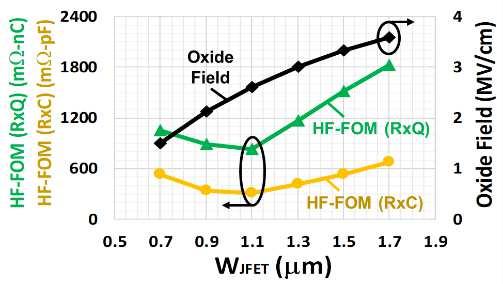
46 SiC Power MOSFET: New OCTFET Cell Topology TABLE I SUMMARY OF EXPERIMENTAL RESULTS FOR THE OCTFETS AND THE CONVENTIONAL LINEAR MOSFET linear_j0.7 O_J0.9 O_J1.1 O_J1.3 O_J1.5 O_J1.1_C CH. density [µm -1 ] JFET density BV [V] V th [V] *R on,sp [mωcm ] C gd,sp [pf/cm 2 ] Q gd,sp [nc/cm 2 ] FOM (Ron Cgd) [mω-pf] FOM (Ron Qgd) [mω-nc] * includes R sub (~0.7 mω-cm 2 ) 2.1x Improvement 1.4x Improvement K. Han and B.J. Baliga, The 1.2 kv 4H-SiC OCTFET: A New Cell Topology with Improved High- Frequency Figures-of-Merit", IEEE Electron Device Letters, Vol. 40, pp , February
47 Outline SiC Power MOSFET Breakthroughs achieved at NCSU PRESiCE: SiC Power Device Manufacturing Technology SiC Power MOSFETs: Inversion Channel & Accumulation Channel The JBSFET: SiC MOSFET with Integrated Schottky Diode Split-Gate (SG) MOSFET: Improved HF-FOM Buffered-Gate (BG) MOSFET: Further Improved HF-FOM The OCTFET: A New Cell Topology with Superior High Frequency Figures-of-Merit The BiDFET: A Monolithic Bi-Directional Field Effect Transistor 47

48 BiDFET: Monolithic Bi-Directional FET 48


49 Proposed SiC Bi-Directional FET BiDFET Drain Metal Drain Metal Drain Metal 49

50 BiDFET: Experimental Results 50
51 BiDFET: Experimental Results 51
52 BiDFET: Experimental Results 52
 IGBT On-State Voltage Drop = 2.5 V SiC Diode On-State Voltage Drop = 1.5 V SiC MOSFET On-State Voltage Drop = 0.")
53 BiDFET: Comparison with Prior Art Assumptions: Si Diode On-State Voltage Drop = 1.5 V Si Asymmetric IGBT On-State Voltage Drop = 2.0 V Si Symmetric (RB) IGBT On-State Voltage Drop = 2.5 V SiC Diode On-State Voltage Drop = 1.5 V SiC MOSFET On-State Voltage Drop = 0.25 V 53


54 BiDFET: Monolithic Bi-Directional FET B.J. Baliga and K. Han, "Monolithic SiC Bi-Directional Field Effect Transistor (BiDFET): Concept, Implementation, and Electrical Characteristics ", GOMACTech 2018, Paper 3.2, pp , March 13,
55 Conclusion SiC Power MOSFET Breakthroughs achieved at NCSU PRESiCE: SiC Power Device Manufacturing Technology SiC Power MOSFETs: Inversion Channel & Accumulation Channel The JBSFET: SiC MOSFET with Integrated Schottky Diode Split-Gate (SG) MOSFET: Improved HF-FOM Buffered-Gate (BG) MOSFET: Further Improved HF-FOM The OCTFET: A New Cell Topology with Superior High Frequency Figures-of-Merit The BiDFET: A Monolithic Bi-Directional Field Effect Transistor 55
Power MOSFET Zheng Yang (ERF 3017,
 ECE442 Power Semiconductor Devices and Integrated Circuits Power MOSFET Zheng Yang (ERF 3017, email: yangzhen@uic.edu) Evolution of low-voltage (
Students: Yifan Jiang (Research Assistant) Siyang Liu (Visiting Scholar)
 Siyang Liu (Visiting Scholar)") Y9.FS1.1: SiC Power Devices for SST Applications Project Leader: Faculty: Dr. Jayant Baliga Dr. Alex Huang Students: Yifan Jiang (Research Assistant) Siyang Liu (Visiting Scholar) 1. Project Goals (a)
Y9.FS1.1: SiC Power Devices for SST Applications Project Leader: Faculty: Dr. Jayant Baliga Dr. Alex Huang Students: Yifan Jiang (Research Assistant) Siyang Liu (Visiting Scholar) 1. Project Goals (a)
Advanced Power MOSFET Concepts
 В. Jayant Baliga Advanced Power MOSFET Concepts Springer Contents 1 Introduction 1 1.1 Ideal Power Switching Waveforms 2 1.2 Ideal and Typical Power MOSFET Characteristics 3 1.3 Typical Power MOSFET Structures
Fundamentals of Power Semiconductor Devices
 В. Jayant Baliga Fundamentals of Power Semiconductor Devices 4y Spri ringer Contents Preface vii Chapter 1 Introduction 1 1.1 Ideal and Typical Power Switching Waveforms 3 1.2 Ideal and Typical Power Device
Y9.FS1.2.1: GaN Low Voltage Power Device Development. Sizhen Wang (Ph.D., EE)
") Y9.FS1.2.1: GaN Low Voltage Power Device Development Faculty: Students: Alex. Q. Huang Sizhen Wang (Ph.D., EE) 1. Project Goals The overall objective of the GaN power device project is to fabricate and
Y9.FS1.2.1: GaN Low Voltage Power Device Development Faculty: Students: Alex. Q. Huang Sizhen Wang (Ph.D., EE) 1. Project Goals The overall objective of the GaN power device project is to fabricate and
Some Key Researches on SiC Device Technologies and their Predicted Advantages
 18 POWER SEMICONDUCTORS www.mitsubishichips.com Some Key Researches on SiC Device Technologies and their Predicted Advantages SiC has proven to be a good candidate as a material for next generation power
USCi MOSFET progress (ARL HVPT program)
") USCi MOSFET progress (ARL HVPT program) L. Fursin, X. Huang, W. Simon, M. Fox, J. Hostetler, X. Li, A. Bhalla Aug 18, 2016 Contents USCi product line 1200V MOSFET progress 10kV IGBT and MPS progress 2
USCi MOSFET progress (ARL HVPT program) L. Fursin, X. Huang, W. Simon, M. Fox, J. Hostetler, X. Li, A. Bhalla Aug 18, 2016 Contents USCi product line 1200V MOSFET progress 10kV IGBT and MPS progress 2
Temperature-Dependent Characterization of SiC Power Electronic Devices
 Temperature-Dependent Characterization of SiC Power Electronic Devices Madhu Sudhan Chinthavali 1 chinthavalim@ornl.gov Burak Ozpineci 2 burak@ieee.org Leon M. Tolbert 2, 3 tolbert@utk.edu 1 Oak Ridge
Wide Band-Gap Power Device
 Wide Band-Gap Power Device 1 Contents Revisit silicon power MOSFETs Silicon limitation Silicon solution Wide Band-Gap material Characteristic of SiC Power Device Characteristic of GaN Power Device 2 1
High-Temperature and High-Frequency Performance Evaluation of 4H-SiC Unipolar Power Devices
 High-Temperature and High-Frequency Performance Evaluation of H-SiC Unipolar Power Devices Madhu Sudhan Chinthavali Oak Ridge Institute for Science and Education Oak Ridge, TN 37831-117 USA chinthavalim@ornl.gov
Monolithic integration of GaN power transistors integrated with gate drivers
 October 3-5, 2016 International Workshop on Power Supply On Chip (PwrSoC 2016) Monolithic integration of GaN power transistors integrated with gate drivers October 4, 2016 Tatsuo Morita Automotive & Industrial
Chapter 9 SiC Planar MOSFET Structures
 Chapter 9 SiC Planar MOSFET Structures In Chap. 1, it was demonstrated that the specific on-resistance of power MOSFET devices can be greatly reduced by replacing silicon with wide band gap semiconductors.
4H-SiC V-Groove Trench MOSFETs with the Buried p + Regions
 ELECTRONICS 4H-SiC V-Groove Trench MOSFETs with the Buried p + Regions Yu SAITOH*, Toru HIYOSHI, Keiji WADA, Takeyoshi MASUDA, Takashi TSUNO and Yasuki MIKAMURA ----------------------------------------------------------------------------------------------------------------------------------------------------------------------------------------------------------------------------------------------------------
SGP100N09T. Symbol Parameter SGP100N09T Unit. 70* -Continuous (TA = 100 )
") SUPER-SEMI SUPER-MOSFET Super Gate Metal Oxide Semiconductor Field Effect Transistor 100V Super Gate Power Transistor SG*100N09T Rev. 1.01 Jun. 2016 SGP100N09T 100V N-Channel MOSFET Description The SG-MOSFET
SUPER-SEMI SUPER-MOSFET Super Gate Metal Oxide Semiconductor Field Effect Transistor 100V Super Gate Power Transistor SG*100N09T Rev. 1.01 Jun. 2016 SGP100N09T 100V N-Channel MOSFET Description The SG-MOSFET
Introduction Device Achievements & Needs Future Prospects of SiC Power Devices Conclusion
 Present Present Status Status And And Future Future Prospects of of SiC SiC Power Power Devices Devices Contributors : Gourab Majumdar Chief Engineer, Power Device Works, Mitsubishi Electric Corporation,
Advances in SiC Power Technology
 Advances in SiC Power Technology DARPA MTO Symposium San Jose, CA March 7, 2007 John Palmour David Grider, Anant Agarwal, Brett Hull, Bob Callanan, Jon Zhang, Jim Richmond, Mrinal Das, Joe Sumakeris, Adrian
NAME: Last First Signature
 UNIVERSITY OF CALIFORNIA, BERKELEY College of Engineering Department of Electrical Engineering and Computer Sciences EE 130: IC Devices Spring 2003 FINAL EXAMINATION NAME: Last First Signature STUDENT
ENHANCING POWER ELECTRONIC DEVICES WITH WIDE BANDGAP SEMICONDUCTORS
 ENHANCING POWER ELECTRONIC DEVICES WITH WIDE BANDGAP SEMICONDUCTORS BURAK OZPINECI Oak Ridge National Laboratory Oak Ridge, TN 37831-6472 USA ozpinecib@ornl.gov MADHU SUDHAN CHINTHAVALI Oak Ridge Institute
ECSE-6300 IC Fabrication Laboratory Lecture 7 MOSFETs. Lecture Outline
 ECSE-6300 IC Fabrication Laboratory Lecture 7 MOSFETs Prof. Rensselaer Polytechnic Institute Troy, NY 12180 Office: CII-6229 Tel.: (518) 276-2909 e-mails: luj@rpi.edu http://www.ecse.rpi.edu/courses/s16/ecse
ECE 5745 Complex Digital ASIC Design Topic 2: CMOS Devices
 ECE 5745 Complex Digital ASIC Design Topic 2: CMOS Devices Christopher Batten School of Electrical and Computer Engineering Cornell University http://www.csl.cornell.edu/courses/ece5950 Simple Transistor
MOSFET & IC Basics - GATE Problems (Part - I)
") MOSFET & IC Basics - GATE Problems (Part - I) 1. Channel current is reduced on application of a more positive voltage to the GATE of the depletion mode n channel MOSFET. (True/False) [GATE 1994: 1 Mark]
MOSFET & IC Basics - GATE Problems (Part - I) 1. Channel current is reduced on application of a more positive voltage to the GATE of the depletion mode n channel MOSFET. (True/False) [GATE 1994: 1 Mark]
Three Terminal Devices
 Three Terminal Devices - field effect transistor (FET) - bipolar junction transistor (BJT) - foundation on which modern electronics is built - active devices - devices described completely by considering
PWRLITE LD1010D High Performance N-Ch Vertical Power JFET Transistor with Schottky G D S
 www.lovoltech.com PWRLITE LD11D High Performance N-Ch Vertical Power JFET Transistor with Schottky Features Trench Power JFET with low threshold voltage Vth. Device fully ON with Vgs =.7V Optimum for Low
M?k^iMMIBiiS^^^M^^Ä^^^ÄÄ^I^^^ÄyM»ÄM^SSSäSä^^iB^S^«SI^M^^«^B^^^^^» ANNUAL REPORT. Novel SiC High Power IC
 M?k^iMMIBiiS^^^M^^Ä^^^ÄÄ^I^^^ÄyM»ÄM^SSSäSä^^iB^S^«SI^M^^«^B^^^^^» ANNUAL REPORT Novel SiC High Power IC Tehnology Supported Under Grant # N00014-98-1-0534 Office of Naval Research Funded by DARPA/ETO Program
Power FINFET, a Novel Superjunction Power MOSFET
 Power FINFET, a Novel Superjunction Power MOSFET Wai Tung Ng Smart Power Integration & Semiconductor Devices Research Group Department of Electrical and Computer Engineering Toronto, Ontario Canada, M5S
D AB Z DETAIL "B" DETAIL "A"
 QJD1211 Preliminary Powerex, Inc., 173 Pavilion Lane, Youngwood, Pennsylvania 15697 (724) 925-7272 www.pwrx.com Split Dual SiC MOSFET Module 1 Amperes/12 Volts Y A AA F D AB Z AC Q DETAIL "B" Q P Q U B
ECSE-6300 IC Fabrication Laboratory Lecture 9 MOSFETs. Lecture Outline
 ECSE-6300 IC Fabrication Laboratory Lecture 9 MOSFETs Prof. Rensselaer Polytechnic Institute Troy, NY 12180 Office: CII-6229 Tel.: (518) 276-2909 e-mails: luj@rpi.edu http://www.ecse.rpi.edu/courses/s18/ecse
Q1. Explain the construction and principle of operation of N-Channel and P-Channel Junction Field Effect Transistor (JFET).
.") Q. Explain the construction and principle of operation of N-Channel and P-Channel Junction Field Effect Transistor (JFET). Answer: N-Channel Junction Field Effect Transistor (JFET) Construction: Drain(D)
Q. Explain the construction and principle of operation of N-Channel and P-Channel Junction Field Effect Transistor (JFET). Answer: N-Channel Junction Field Effect Transistor (JFET) Construction: Drain(D)
A new Vertical JFET Technology for Harsh Radiation Applications
 A New Vertical JFET Technology for Harsh Radiation Applications ISPS 2016 1 A new Vertical JFET Technology for Harsh Radiation Applications A Rad-Hard switch for the ATLAS Inner Tracker P. Fernández-Martínez,
High Voltage Normally-off GaN MOSC- HEMTs on Silicon Substrates for Power Switching Applications
 High Voltage Normally-off GaN MOSC- HEMTs on Silicon Substrates for Power Switching Applications Zhongda Li, John Waldron, Shinya Takashima, Rohan Dayal, Leila Parsa, Mona Hella, and T. Paul Chow Department
Improving Totem-Pole PFC and On Board Charger performance with next generation components
 Improving Totem-Pole PFC and On Board Charger performance with next generation components Anup Bhalla 1) 1) United Silicon Carbide, Inc., 7 Deer Park Drive, Monmouth Jn., NJ USA E-mail: abhalla@unitedsic.com
SiC Cascodes and its advantages in power electronic applications
 SiC Cascodes and its advantages in power electronic applications WBG Power Conference, Munich, 5 th December 2017 Christopher Rocneanu Director Sales Europe and North America cro@unitedsic.com +4915121063411
Impact of Basal Plane Dislocations and Ruggedness of 10 kv 4H-SiC Transistors
 11th International MOS-AK Workshop (co-located with the IEDM and CMC Meetings) Silicon Valley, December 5, 2018 Impact of Basal Plane Dislocations and Ruggedness of 10 kv 4H-SiC Transistors *, A. Kumar,
GaN is Crushing Silicon. EPC - The Leader in GaN Technology IEEE PELS
 GaN is Crushing Silicon EPC - The Leader in GaN Technology IEEE PELS 2014 www.epc-co.com 1 Agenda How egan FETs work Hard Switched DC-DC converters High Efficiency point-of-load converter Envelope Tracking
3-D Modelling of the Novel Nanoscale Screen-Grid Field Effect Transistor (SGFET)
") 3-D Modelling of the Novel Nanoscale Screen-Grid Field Effect Transistor (SGFET) Pei W. Ding, Kristel Fobelets Department of Electrical Engineering, Imperial College London, U.K. J. E. Velazquez-Perez
3-D Modelling of the Novel Nanoscale Screen-Grid Field Effect Transistor (SGFET) Pei W. Ding, Kristel Fobelets Department of Electrical Engineering, Imperial College London, U.K. J. E. Velazquez-Perez
Advanced Silicon Devices Applications and Technology Trends
 Advanced Silicon Devices Applications and Technology Trends Gerald Deboy Winfried Kaindl, Uwe Kirchner, Matteo Kutschak, Eric Persson, Michael Treu APEC 2015 Content Silicon devices versus GaN devices:
GaAs PowerStages for Very High Frequency Power Supplies. Greg Miller Sr. VP - Engineering Sarda Technologies
 GaAs PowerStages for Very High Frequency Power Supplies Greg Miller Sr. VP - Engineering Sarda Technologies gmiller@sardatech.com Agenda Case for Higher Power Density Voltage Regulators Limitations of
Unit III FET and its Applications. 2 Marks Questions and Answers
 Unit III FET and its Applications 2 Marks Questions and Answers 1. Why do you call FET as field effect transistor? The name field effect is derived from the fact that the current is controlled by an electric
Study on Fabrication and Fast Switching of High Voltage SiC JFET
 Advanced Materials Research Online: 2013-10-31 ISSN: 1662-8985, Vol. 827, pp 282-286 doi:10.4028/www.scientific.net/amr.827.282 2014 Trans Tech Publications, Switzerland Study on Fabrication and Fast Switching
3084 IEEE TRANSACTIONS ON NUCLEAR SCIENCE, VOL. 60, NO. 4, AUGUST 2013
 3084 IEEE TRANSACTIONS ON NUCLEAR SCIENCE, VOL. 60, NO. 4, AUGUST 2013 Dummy Gate-Assisted n-mosfet Layout for a Radiation-Tolerant Integrated Circuit Min Su Lee and Hee Chul Lee Abstract A dummy gate-assisted
Field-Effect Transistor (FET) is one of the two major transistors; FET derives its name from its working mechanism;
 is one of the two major transistors; FET derives its name from its working mechanism;") Chapter 3 Field-Effect Transistors (FETs) 3.1 Introduction Field-Effect Transistor (FET) is one of the two major transistors; FET derives its name from its working mechanism; The concept has been known
Chapter 3 Field-Effect Transistors (FETs) 3.1 Introduction Field-Effect Transistor (FET) is one of the two major transistors; FET derives its name from its working mechanism; The concept has been known
Basic Fabrication Steps
 Basic Fabrication Steps and Layout Somayyeh Koohi Department of Computer Engineering Adapted with modifications from lecture notes prepared by author Outline Fabrication steps Transistor structures Transistor
A 1-kV 4H-SiC power DMOSFET optimized for low ON-resistance
 Purdue University Purdue e-pubs Birck and NCN Publications Birck Nanotechnology Center October 2007 A 1-kV 4H-SiC power DMOSFET optimized for low ON-resistance Asmita Saha Purdue University James A. Cooper
Reaching new heights by producing 1200V SiC MOSFETs in CMOS fab
 82 Technology focus: Silicon carbide Reaching new heights by producing 1200V SiC MOSFETs in CMOS fab Monolith Semiconductor and Littelfuse describe how 1200V silicon carbide MOSFETs can be mass produced
SiC Transistor Basics: FAQs
 SiC Transistor Basics: FAQs Silicon Carbide (SiC) MOSFETs exhibit higher blocking voltage, lower on state resistance and higher thermal conductivity than their silicon counterparts. Oct. 9, 2013 Sam Davis
Open Access. C.H. Ho 1, F.T. Chien 2, C.N. Liao 1 and Y.T. Tsai*,1
 56 The Open Electrical and Electronic Engineering Journal, 2008, 2, 56-61 Open Access Optimum Design for Eliminating Back Gate Bias Effect of Silicon-oninsulator Lateral Double Diffused Metal-oxide-semiconductor
ELEC-E8421 Components of Power Electronics
 ELEC-E8421 Components of Power Electronics MOSFET 2015-10-04 Metal-Oxide-Semiconductor Field-Effect-Transistor (MOSFET) Vertical structure makes paralleling of many small MOSFETs on the chip easy. Very
Depletion-mode operation ( 공핍형 ): Using an input gate voltage to effectively decrease the channel size of an FET
: Using an input gate voltage to effectively decrease the channel size of an FET") Ch. 13 MOSFET Metal-Oxide-Semiconductor Field-Effect Transistor : I D D-mode E-mode V g The gate oxide is made of dielectric SiO 2 with e = 3.9 Depletion-mode operation ( 공핍형 ): Using an input gate voltage
Ch. 13 MOSFET Metal-Oxide-Semiconductor Field-Effect Transistor : I D D-mode E-mode V g The gate oxide is made of dielectric SiO 2 with e = 3.9 Depletion-mode operation ( 공핍형 ): Using an input gate voltage
Electrical Characterization of a Second-gate in a Silicon-on-Insulator Transistor
 Electrical Characterization of a Second-gate in a Silicon-on-Insulator Transistor Antonio Oblea: McNair Scholar Dr. Stephen Parke: Faculty Mentor Electrical Engineering As an independent double-gate, silicon-on-insulator
Tests of monolithic CMOS SOI pixel detector prototype INTPIX3 MOHAMMED IMRAN AHMED. Supervisors Dr. Henryk Palka (IFJ-PAN) Dr. Marek Idzik(AGH-UST)
 Dr. Marek Idzik(AGH-UST)") Internal Note IFJ PAN Krakow (SOIPIX) Tests of monolithic CMOS SOI pixel detector prototype INTPIX3 by MOHAMMED IMRAN AHMED Supervisors Dr. Henryk Palka (IFJ-PAN) Dr. Marek Idzik(AGH-UST) Test and Measurement
Internal Note IFJ PAN Krakow (SOIPIX) Tests of monolithic CMOS SOI pixel detector prototype INTPIX3 by MOHAMMED IMRAN AHMED Supervisors Dr. Henryk Palka (IFJ-PAN) Dr. Marek Idzik(AGH-UST) Test and Measurement
MEI. 20V P-Channel Enhancement-Mode MOSFET P2301BLT1G. Features. Simple Drive Requirement Small Package Outline Surface Mount Device G 1 2 V DS -20
 V P-Channel Enhancement-Mode MOSFET VDS= -V RDS(ON), Vgs@-.5V, Ids@-.A = mω RDS(ON), Vgs@-.5V, Ids@-.A = 15 mω Features Advanced trench process technology High Density Cell Design For Ultra Low On-Resistance
GS61008T Top-side cooled 100 V E-mode GaN transistor Preliminary Datasheet
 Features 100 V enhancement mode power switch Top-side cooled configuration R DS(on) = 7 mω I DS(max) = 90 A Ultra-low FOM Island Technology die Low inductance GaNPX package Easy gate drive requirements
Lecture 19 Real Semiconductor Switches and the Evolution of Power MOSFETS A.. Real Switches: I(D) through the switch and V(D) across the switch
 through the switch and V(D) across the switch") Lecture 19 Real Semiconductor Switches and the Evolution of Power MOSFETS 1 A.. Real Switches: I(D) through the switch and V(D) across the switch 1. Two quadrant switch implementation and device choice
Lecture 19 Real Semiconductor Switches and the Evolution of Power MOSFETS 1 A.. Real Switches: I(D) through the switch and V(D) across the switch 1. Two quadrant switch implementation and device choice
Alternative Channel Materials for MOSFET Scaling Below 10nm
 Alternative Channel Materials for MOSFET Scaling Below 10nm Doug Barlage Electrical Requirements of Channel Mark Johnson Challenges With Material Synthesis Introduction Outline Challenges with scaling
INTRODUCTION: Basic operating principle of a MOSFET:
 INTRODUCTION: Along with the Junction Field Effect Transistor (JFET), there is another type of Field Effect Transistor available whose Gate input is electrically insulated from the main current carrying
EPC2014 Enhancement Mode Power Transistor
 EPC4 EPC4 Enhancement Mode Power Transistor V DSS, V R DS(ON), 6 mw I D, A NEW PRODUCT EFFICIENT POWER CONVERSION HAL Gallium Nitride is grown on Silicon Wafers and processed using standard CMOS equipment
Achieving 3000 V test at the wafer level
 Achieving 3000 V test at the wafer level Bryan Root 1, Alex Pronin 2, Seng Yang 1,Bill Funk 1, K. Armendariz 1 1 Celadon Systems Inc., 2 Keithley September 2016 Outline Introduction Si, SiC and GaN Power
GS61008P Bottom-side cooled 100 V E-mode GaN transistor Preliminary Datasheet
 Features 100 V enhancement mode power switch Bottom-side cooled configuration R DS(on) = 7 mω I DS(max) = 90 A Ultra-low FOM Island Technology die Low inductance GaNPX package Easy gate drive requirements
Analog and Telecommunication Electronics
 Politecnico di Torino - ICT School Analog and Telecommunication Electronics F2 Active power devices»mos»bjt» IGBT, TRIAC» Safe Operating Area» Thermal analysis 30/05/2012-1 ATLCE - F2-2011 DDC Lesson F2:
Design of a Rugged 60V VDMOS Transistor
 Design of a Rugged 60V VDMOS Transistor H. P. Edward Xu, Olivier P. Trescases, I-Shan Michael Sun, Dora Lee, Wai Tung Ng*, Kenji Fukumoto, Akira Ishikawa, Yuichi Furukawa, Hisaya Imai, Takashi Naito, Nobuyuki
GaN based Power Devices. Michael A. Briere. RPI CFES Conference
 GaN based Power Devices Michael A. Briere ACOO Enterprises LLC Under contract to International Rectifier RPI CFES Conference January 25, 2013 1 Motivation : Potential Energy Savings Worldwide M.A. Briere
Gallium nitride (GaN)
") 80 Technology focus: GaN power electronics Vertical, CMOS and dual-gate approaches to gallium nitride power electronics US research company HRL Laboratories has published a number of papers concerning
80 Technology focus: GaN power electronics Vertical, CMOS and dual-gate approaches to gallium nitride power electronics US research company HRL Laboratories has published a number of papers concerning
Appendix: Power Loss Calculation
 Appendix: Power Loss Calculation Current flow paths in a synchronous buck converter during on and off phases are illustrated in Fig. 1. It has to be noticed that following parameters are interrelated:
Monolith Semiconductor Inc. ARL SiC MOSFET Workshop 14 August 2015
 Monolith Semiconductor Inc. ARL SiC MOSFET Workshop 14 August 2015 Kevin Matocha, President 408 Fannin Ave Round Rock, TX 78664 Bringing SiC to our World. Acknowledgments Office of Science SBIR Prog. Office
Solid State Device Fundamentals
 Solid State Device Fundamentals 4.4. Field Effect Transistor (MOSFET) ENS 463 Lecture Course by Alexander M. Zaitsev alexander.zaitsev@csi.cuny.edu Tel: 718 982 2812 4N101b 1 Field-effect transistor (FET)
VDS (V) min 600 VTDS (V) max 750 RDS(on) (mω) max* 63. Qrr (nc) typ 136. * Dynamic R(on)
 min 600 VTDS (V) max 750 RDS(on) (mω) max* 63. Qrr (nc) typ 136. * Dynamic R(on)") 600V Cascode GaN FET in TO-247 (source tab) Not recommended for new designs see TP65H050WS Description The TPH3205WS 600V, 52mΩ gallium nitride (GaN) FET is a normally-off device. Transphorm GaN FETs offer
600V Cascode GaN FET in TO-247 (source tab) Not recommended for new designs see TP65H050WS Description The TPH3205WS 600V, 52mΩ gallium nitride (GaN) FET is a normally-off device. Transphorm GaN FETs offer
SSF6602. Main Product Characteristics. Features and Benefits. Description. Absolute Maximum Ratings (T A =25 C unless otherwise specified)
") Main Product Characteristics D2 S1 V (BR)DSS 30V -30V D1 58mΩ@10V 100mΩ@-10V G2 R DS(on)MAX 95mΩ@4.5V 150mΩ@-4.5V G1 S2 I D 3.5A -2.7A SOT-23-6L Schematic Diagram Features and Benefits Advanced MOSFET
Main Product Characteristics D2 S1 V (BR)DSS 30V -30V D1 58mΩ@10V 100mΩ@-10V G2 R DS(on)MAX 95mΩ@4.5V 150mΩ@-4.5V G1 S2 I D 3.5A -2.7A SOT-23-6L Schematic Diagram Features and Benefits Advanced MOSFET
Comparison of SiC and Si Power Semiconductor Devices to Be Used in 2.5 kw DC/DC Converter
 Comparison of SiC and Si Power Semiconductor Devices to Be Used in 2.5 kw DC/DC Converter M. G. Hosseini Aghdam Division of Electric Power Engineering Department of Energy and Environment Chalmers University
General look back at MESFET processing. General principles of heterostructure use in FETs
 SMA5111 - Compound Semiconductors Lecture 11 - Heterojunction FETs - General HJFETs, HFETs Last items from Lec. 10 Depletion mode vs enhancement mode logic Complementary FET logic (none exists, or is likely
Low On-Resistance Trench Lateral Power MOS Technology
 Low On-Resistance Trench Lateral Power MO Technology Akio ugi Mutsumi awada Naoto Fujishima 1. Introduction Market demands for smaller sized, lighter weight, lower power consuming and higher efficiency
Wide band gap, (GaN, SiC etc.) device evaluation with the Agilent B1505A Accelerate emerging material device development
 device evaluation with the Agilent B1505A Accelerate emerging material device development") Wide band gap, (GaN, SiC etc.) device evaluation with the Agilent B1505A Accelerate emerging material device development Stewart Wilson European Sales Manager Semiconductor Parametric Test Systems Autumn
Wide band gap, (GaN, SiC etc.) device evaluation with the Agilent B1505A Accelerate emerging material device development Stewart Wilson European Sales Manager Semiconductor Parametric Test Systems Autumn
Review of Power IC Technologies
 Review of Power IC Technologies Ettore Napoli Dept. Electronic and Telecommunication Engineering University of Napoli, Italy Introduction The integration of Power and control circuitry is desirable for
Pitch Pack Microsemi full SiC Power Modules
 Pitch Pack Microsemi full SiC Power Modules October 2014 SiC Main Characteristics vs. Si Characteristics SiC vs. Si Results Benefits Breakdown field (MV/cm) Electron sat. velocity (cm/s) Bandgap energy
FIELD EFFECT TRANSISTOR (FET) 1. JUNCTION FIELD EFFECT TRANSISTOR (JFET)
 1. JUNCTION FIELD EFFECT TRANSISTOR (JFET)") FIELD EFFECT TRANSISTOR (FET) The field-effect transistor (FET) is a three-terminal device used for a variety of applications that match, to a large extent, those of the BJT transistor. Although there
FIELD EFFECT TRANSISTOR (FET) The field-effect transistor (FET) is a three-terminal device used for a variety of applications that match, to a large extent, those of the BJT transistor. Although there
Characterization and Modeling of 4H-SiC Low Voltage MOSFETs and Power MOSFETs
 University of Arkansas, Fayetteville ScholarWorks@UARK Theses and Dissertations 5-2012 Characterization and Modeling of 4H-SiC Low Voltage MOSFETs and Power MOSFETs Mihir Mudholkar University of Arkansas,
Next Generation Curve Tracing & Measurement Tips for Power Device. Kim Jeong Tae RF/uW Application Engineer Keysight Technologies
 Next Generation Curve Tracing & Measurement Tips for Power Device Kim Jeong Tae RF/uW Application Engineer Keysight Technologies Agenda Page 2 Conventional Analog Curve Tracer & Measurement Challenges
WPM3028 WPM3028. Descriptions. Features. Applications. Order information. Typical R DS(on) (mω) V GS =-10V V GS =-5V -30
 (mω) V GS =-10V V GS =-5V -30") WPM32 WPM32 Single P-Channel, -3V, -11.5A, Power MOSFET Http://www.sh-willsemi.com V DS (V) Typical R DS(on) (mω) -3 11@ =-1V 15 @ =-5V S S S G Descriptions The WPM32 is P-Channel enhancement MOS Field
WPM32 WPM32 Single P-Channel, -3V, -11.5A, Power MOSFET Http://www.sh-willsemi.com V DS (V) Typical R DS(on) (mω) -3 11@ =-1V 15 @ =-5V S S S G Descriptions The WPM32 is P-Channel enhancement MOS Field
VDS (V) min 600 VTDS (V) max 750 RDS(on) (mω) max* 180. Qrr (nc) typ 54. * Dynamic R(on)
 min 600 VTDS (V) max 750 RDS(on) (mω) max* 180. Qrr (nc) typ 54. * Dynamic R(on)") 600V Cascode GaN FET in TO-220 (drain tab) Description The 600V, 150mΩ gallium nitride (GaN) FET is a normally-off device. Transphorm GaN FETs offer better efficiency through lower gate charge, faster
600V Cascode GaN FET in TO-220 (drain tab) Description The 600V, 150mΩ gallium nitride (GaN) FET is a normally-off device. Transphorm GaN FETs offer better efficiency through lower gate charge, faster
SIMULATION STUDIES OF HALF-BRIDGE ISOLATED DC/DC BOOST CONVERTER
 POZNAN UNIVE RSITY OF TE CHNOLOGY ACADE MIC JOURNALS No 80 Electrical Engineering 2014 Adam KRUPA* SIMULATION STUDIES OF HALF-BRIDGE ISOLATED DC/DC BOOST CONVERTER In order to utilize energy from low voltage
GS61008T Top-side cooled 100 V E-mode GaN transistor Preliminary Datasheet
 Features 100 V enhancement mode power switch Top-side cooled configuration R DS(on) = 7 mω I DS(max) = 90 A Ultra-low FOM Island Technology die Low inductance GaNPX package Easy gate drive requirements
All-SiC Modules Equipped with SiC Trench Gate MOSFETs
 All-SiC Modules Equipped with SiC Trench Gate MOSFETs NAKAZAWA, Masayoshi * DAICHO, Norihiro * TSUJI, Takashi * A B S T R A C T There are increasing expectations placed on products that utilize SiC modules
Complementary MOSFET
 General Description uses advanced trench technology to provide excellent Rds(on) and low gate charge. Complementary MOSFET Features N-channel Vds=40V, Id=8.0A, Rds(on)=22mΩ(Vgs=10V) Vds=40V, Id=6.0A, Rds(on)=28mΩ(Vgs=4.5V)
Taiwan Goodark Technology Co.,Ltd TGD0103M
 TGD N-Channel Enhancement Mode Power MOSFET Description The uses advanced trench technology and design to provide excellent R DS(ON) with low gate charge. It can be used in a wide variety of applications.
ALL Switch GaN Power Switch - DAS V22N65A
 Description ALL-Switch is a System In Package (SIP) switch. A Normally-Off safe function is integrated within the package, designed according to SmartGaN topology, an innovation by VisIC Technologies.
Trench MOS Having Source with Waffle Patterns
 POSTER 2018, PRAGUE MAY 10 1 Trench MOS Having Source with Waffle Patterns Patrik VACULA 1, 2, Vlastimil KOTĚ 1, 2, Dalibor BARRI 1, 2 1 Dept. of Microelectronics, Czech Technical University, Technická
2nd-Generation Low Loss SJ-MOSFET with Built-In Fast Diode Super J MOS S2FD Series
 2nd-Generation Low Loss SJ-MOSFET with Built-In Fast Diode Super J MOS WATANABE, Sota * SAKATA, Toshiaki * YAMASHITA, Chiho * A B S T R A C T In order to make efficient use of energy, there has been increasing
EPE 2005 Dresden ESCAPEE. ESCAPEE Project. SiC Workshop. EPE 2005, September 12
 1 EPE 2005 Dresden ESCAPEE 2 The achievements of the EC funded project "Establish Silicon Carbide Applications for Power Electronics in Europe" (ESCAPEE) J. Millan 1, P. Godignon 1, D. Tournier 1, P.A.
Transistor Scaling in the Innovation Era. Mark Bohr Intel Senior Fellow Logic Technology Development August 15, 2011
 Transistor Scaling in the Innovation Era Mark Bohr Intel Senior Fellow Logic Technology Development August 15, 2011 MOSFET Scaling Device or Circuit Parameter Scaling Factor Device dimension tox, L, W
Power Matters Microsemi SiC Products
 Microsemi SiC Products James Kerr Director of Marketing Power Discrete Products Microsemi Power Products MOSFETs (100V-1200V) Highest Performance SiC MOSFETs 1200V MOSFETs FREDFETs (MOSFET with fast body
Drive and Layout Requirements for Fast Switching High Voltage MOSFETs
 Drive and Layout Requirements for Fast Switching High Voltage MOSFETs Contents Introduction SuperJunction Technologies Influence of Circuit Parameters on Switching Characteristics Gate Resistance Clamp
n-channel LDMOS WITH STI FOR BREAKDOWN VOLTAGE ENHANCEMENT AND IMPROVED R ON
 n-channel LDMOS WITH STI FOR BREAKDOWN VOLTAGE ENHANCEMENT AND IMPROVED R ON 1 SUNITHA HD, 2 KESHAVENI N 1 Asstt Prof., Department of Electronics Engineering, EPCET, Bangalore 2 Prof., Department of Electronics
PERSPECTIVES FOR DISRUPTIVE 200MM/8-INCH GAN POWER DEVICE AND GAN-IC TECHNOLOGY DR. DENIS MARCON SR. BUSINESS DEVELOPMENT MANAGER
 PERSPECTIVES FOR DISRUPTIVE 200MM/8-INCH GAN POWER DEVICE AND GAN-IC TECHNOLOGY DR. DENIS MARCON SR. BUSINESS DEVELOPMENT MANAGER What I will show you today 200mm/8-inch GaN-on-Si e-mode/normally-off technology
New Wide Band Gap High-Power Semiconductor Measurement Techniques Accelerate your emerging material device development
 New Wide Band Gap High-Power Semiconductor Measurement Techniques Accelerate your emerging material device development Alan Wadsworth Americas Market Development Manager Semiconductor Test Division July
PWRLITE LU1014D High Performance N-Channel POWERJFET TM with PN Diode
 PWRLITE LU114D High Performance N-Channel POWERJFET TM with PN Diode Features Superior gate charge x Rdson product (FOM) Trench Power JFET with low threshold voltage Vth. Device fully ON with Vgs =.7V
1200 V SiC Super Junction Transistors operating at 250 C with extremely low energy losses for power conversion applications
 1200 V SiC Super Junction Transistors operating at 250 C with extremely low energy losses for power conversion applications Ranbir Singh, Siddarth Sundaresan, Eric Lieser and Michael Digangi GeneSiC Semiconductor,
V DSS R DS(on) max Qg (typ.) 60V GS = 10V 24nC
 max Qg (typ.) 60V GS = 10V 24nC") Applications l Synchronous Rectifier MOSFET for Isolated DC-DC Converters l Low Power Motor Drive Systems PD - 97436 IRF735PbF HEXFET Power MOSFET V DSS R DS(on) max Qg (typ.) 60V 7.8mΩ@V GS = 0V 24nC
Applications l Synchronous Rectifier MOSFET for Isolated DC-DC Converters l Low Power Motor Drive Systems PD - 97436 IRF735PbF HEXFET Power MOSFET V DSS R DS(on) max Qg (typ.) 60V 7.8mΩ@V GS = 0V 24nC
6. LDD Design Tradeoffs on Latch-Up and Degradation in SOI MOSFET
 110 6. LDD Design Tradeoffs on Latch-Up and Degradation in SOI MOSFET An experimental study has been conducted on the design of fully depleted accumulation mode SOI (SIMOX) MOSFET with regard to hot carrier
ECE 340 Lecture 37 : Metal- Insulator-Semiconductor FET Class Outline:
 ECE 340 Lecture 37 : Metal- Insulator-Semiconductor FET Class Outline: Metal-Semiconductor Junctions MOSFET Basic Operation MOS Capacitor Things you should know when you leave Key Questions What is the
EPC2007C Enhancement Mode Power Transistor
 EPC7C EPC7C Enhancement Mode Power Transistor V DSS, V R DS(on), 3 mw I D, 6 A NEW PRODUCT EFFICIENT POWER CONVERSION HAL Gallium Nitride is grown on Silicon Wafers and processed using standard CMOS equipment
Taiwan Goodark Technology Co.,Ltd
 TGD N-Channel Enhancement Mode Power MOSFET Description The uses advanced trench technology and design to provide excellent R DS(ON) with low gate charge. It can be used in a wide variety of applications.