STM RH-ASIC capability
|
|
|
- Verity Joan Carroll
- 6 years ago
- Views:
Transcription
1 STM RH-ASIC capability JAXA 24 th MicroElectronic Workshop 13 th 14 th October 2011 Prepared by STM Crolles and AeroSpace Unit
2 Deep Sub Micron (DSM) is strategic for Europe Strategic importance of European DSM access / Support: Scientific satellites and probes require more and more low power RH Computing capability Same trend for Observation satellites Commercial Telecomm satellites progressively move from «listen & retransmit» birds to complex re-programming, signal reconstitution and so on: Computer power needed Business for Telecomm Operators and Satellite makers must strategically not depend from abroad technology sources. European Community (FP-7 Plans) recognized this major risk since 2006 CNES and ESA do technically and financially support this initiative since 2007 RH 65nm STm technology selected in 2009 after successful Reliability and Radiation performance evaluation contracts. European Satellite makers Industry also joined the team STM a 55,000 people advanced technology Company supports European goals This Presentation focuses upon RH, RH Library and Design tools 2


3 ST 65nm CMOS selected by European Space Agencies 21 ST qualification circuits in CMOS 130/90/65/45/40 jointly irradiated by ESA and ST-Crolles since 2005 with heavy ions, protons and gamma rays using ESA certified beam facilities & test standards >1,000,000 test data collected over the past 5 years High intrinsic radiation hardness measured with heavy ions and protons no latch-up nor permanent fails ESA newton spacecraft 2014 Quasi intrinsic immunity to gamma rays no longer need for costly edgeless transistors, rings, Validation of new specific rad-hard solutions and telecom circuits in progress joint work with European satellite makers 3
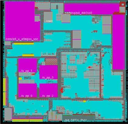


4 ST System-on-Chip approach Memories Digital Logic Data Converters Clock Generator Links & Interfaces Sensors, Regulators Design Methodologies & Design Flows Silicon Validation & Qualification 4


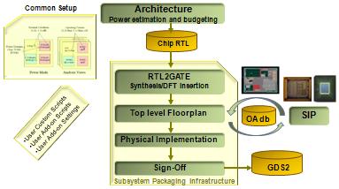
5 Design Flow Overview Common Setup Architecture Power estimation and budgeting Chip RTL RTL to Gate Synthesis/DFT Insertion Top level Prototyping & Floorplan Physical Units Implementation Chip Level Assembly Sign-Off Subsystem Packaging infrastructure GDS2 5
6 Analog / Full Custom Design Flow Overview Design Kit Create schematic Pre-layout simulation Physical Design Kit, analog design Layout creation Layout verification Post layout simulation Custom Methodologies for design robustness, parametric yield enhancement DFM Analysis & Correction Design productivity enhancement Layout finishing


 FIT simulation")


7 Radiation Hardening Design Solutions Expertise covering radiation testing, modeling, hardening Test Chips Modeling Accelerated Rad Test (Crolles) FIT simulation Radiation Hardening Offer Fault Injection platform Real Time Rad Test (Pic de Bure) Rad-hard libraries Radiations Safety and Security Several M$ investments (Y99-11 / 130nm-32nm) Soft Error Simulations at SoC Level Medical Network Automotive Space HDD Printer Mobile Computer 10 team members at ST-Crolles 7


8 Radiation Robust ensured during IP Qualification IP radiation performances mastered with advanced simulations and irradiations Radiation qualification part of IP certification, ST differentiation for automotive, network, medical applications Highest Robustness with patented Rad-Hard Technology Specific design platform for space built-up for several years Chip under irradiation SRAM Fault Injection 8


9 Rard-Hard DSM CMOS65LP schedule Validated Rad-Hard Platform for key Users : Mid First Part: Hardening methodology validated Std cells & Memory in Fab, Second Part, PLL and HSSL : Characterization : 1Q12 Library availability : 2Q12 Completion of equiv-to-20year Reliability Test : 3Q12 Key Open Point : High pin count Packaging 9
10 Conclusions on STM RH-ASIC capability Expertise in testing +50 circuits already characterized over 10 technology nodes 250nm - 28nm state-of-the-art test system and test algorithms compliant with international radiation test standards: ESA-SCC / JEDEC Original & Proprietary analysis solutions to master IP radiation performances in production flow to optimize hardening strategy before silicon State-of-the-art Rad-hard Design Platform CMOS65LP coming up extended corners for space (20 C), several VT flavors rad-hard IO s and PLL high performance standard cells ECC/EDAC-protected SRAM and ROM Leading-Edge Space Cell Libraries (HSSL) 10
Low Power Radiation Tolerant CMOS Design using Commercial Fabrication Processes
 Low Power Radiation Tolerant CMOS Design using Commercial Fabrication Processes Amir Hasanbegovic (amirh@ifi.uio.no) Nanoelectronics Group, Dept. of Informatics, University of Oslo November 5, 2010 Overview
FIRST TELECOM APPLICATION OF DIGITAL AND MIXED COMPONENT DEVELOPMENTS: 65NM ASIC AND DATA CONVERTERS
 AMICSA 2016 FIRST TELECOM APPLICATION OF DIGITAL AND MIXED COMPONENT DEVELOPMENTS: 65NM ASIC AND DATA CONVERTERS F. MALOU, C. AMIOT-BAZILE (CNES), P. VOISIN (TAS) 15th June, 2016 1 Outline FAST project
Mixed Signal Virtual Components COLINE, a case study
 Mixed Signal Virtual Components COLINE, a case study J.F. POLLET - DOLPHIN INTEGRATION Meylan - FRANCE http://www.dolphin.fr Overview of the presentation Introduction COLINE, an example of Mixed Signal
DATE 2016 Early Reliability Modeling for Aging and Variability in Silicon System (ERMAVSS Workshop)
") March 2016 DATE 2016 Early Reliability Modeling for Aging and Variability in Silicon System (ERMAVSS Workshop) Ron Newhart Distinguished Engineer IBM Corporation March 19, 2016 1 2016 IBM Corporation Background
March 2016 DATE 2016 Early Reliability Modeling for Aging and Variability in Silicon System (ERMAVSS Workshop) Ron Newhart Distinguished Engineer IBM Corporation March 19, 2016 1 2016 IBM Corporation Background
Low Power, Radiation tolerant microelectronics design techniques. Executive Summary REF : ASP-04-BO/PE-476 DATE : 02/11/2004 ISSUE : -/2 PAGE : 1 /18
 ISSUE : -/2 PAGE : 1 /18 Executive Summary Written by Responsibility-Company Date Signature Project team Alcatel Space and Imec Verified by Emmanuel Liegeon ASIC Design Engineer - Study responsible Approved
The 20th Microelectronics Workshop Development status of SOI ASIC / FPGA
 The 20th Microelectronics Workshop Development status of SOI ASIC / FPGA Oct. 30th 2007 Electronic, Mechanical Components and Materials Engineering Group, JAXA H.Shindou Background In 2003, critical EEE
UT90nHBD Hardened-by-Design (HBD) Standard Cell Data Sheet February
 Standard Cell Data Sheet February") Semicustom Products UT90nHBD Hardened-by-Design (HBD) Standard Cell Data Sheet February 2018 www.cobham.com/hirel The most important thing we build is trust FEATURES Up to 50,000,000 2-input NAND equivalent
Semicustom Products UT90nHBD Hardened-by-Design (HBD) Standard Cell Data Sheet February 2018 www.cobham.com/hirel The most important thing we build is trust FEATURES Up to 50,000,000 2-input NAND equivalent
ECSS-Q-HB HANDBOOK Techniques for Radiation Effects Mitigation in ASICs and FPGAs
 ECSS-Q-HB-60-02 HANDBOOK Techniques for Radiation Effects Mitigation in ASICs and FPGAs A. Fernández León Microelectronics Section ESA / ESTEC SEE / MAPLD Workshop May 18-21, 2105 OUTLINE Scope and goals
Si Photonics Technology Platform for High Speed Optical Interconnect. Peter De Dobbelaere 9/17/2012
 Si Photonics Technology Platform for High Speed Optical Interconnect Peter De Dobbelaere 9/17/2012 ECOC 2012 - Luxtera Proprietary www.luxtera.com Overview Luxtera: Introduction Silicon Photonics: Introduction
ASICs Concept to Product
 ASICs Concept to Product Synopsis This course is aimed to provide an opportunity for the participant to acquire comprehensive technical and business insight into the ASIC world. As most of these aspects
Changing the Approach to High Mask Costs
 Changing the Approach to High Mask Costs The ever-rising cost of semiconductor masks is making low-volume production of systems-on-chip (SoCs) economically infeasible. This economic reality limits the
Computer Aided Design of Electronics
 Computer Aided Design of Electronics [Datorstödd Elektronikkonstruktion] Zebo Peng, Petru Eles, and Nima Aghaee Embedded Systems Laboratory IDA, Linköping University www.ida.liu.se/~tdts01 Electronic Systems
Interested candidates, please send your resumes to and indicate the job title in subject field.
 Senior/Test Engineer Responsible for preparing the Production Testpackages (Hardware and Software), and Qualification Testprograms Prepares test specifications and hardware (Probecard, Loadboard) design
More Imaging Luc De Mey - CEO - CMOSIS SA
 More Imaging Luc De Mey - CEO - CMOSIS SA Annual Review / June 28, 2011 More Imaging CMOSIS: Vision & Mission CMOSIS s Business Concept On-Going R&D: More Imaging CMOSIS s Vision Image capture is a key
Course Outcome of M.Tech (VLSI Design)
") Course Outcome of M.Tech (VLSI Design) PVL108: Device Physics and Technology The students are able to: 1. Understand the basic physics of semiconductor devices and the basics theory of PN junction. 2.
Course Outcome of M.Tech (VLSI Design) PVL108: Device Physics and Technology The students are able to: 1. Understand the basic physics of semiconductor devices and the basics theory of PN junction. 2.
XI μm Process Family: The XI10 series is X-Fab's 1.0-micron Modular Silicon-On-Insulator Technology DESCRIPTION
 1.0 μm Process Family: XI10 The XI10 series is X-Fab's 1.0-micron Modular Silicon-On-Insulator Technology DESCRIPTION The XI10 series is X-FAB s 1.0 micron Modular Non-fully Depleted SOI CMOS Technology.
Technology Transfers Opportunities, Process and Risk Mitigation. Radhika Srinivasan, Ph.D. IBM
 Technology Transfers Opportunities, Process and Risk Mitigation Radhika Srinivasan, Ph.D. IBM Abstract Technology Transfer is quintessential to any technology installation or semiconductor fab bring up.
Low Power Design Methods: Design Flows and Kits
 JOINT ADVANCED STUDENT SCHOOL 2011, Moscow Low Power Design Methods: Design Flows and Kits Reported by Shushanik Karapetyan Synopsys Armenia Educational Department State Engineering University of Armenia
Short Course Program
 Short Course Program TECHNIQUES FOR SEE MODELING AND MITIGATION OREGON CONVENTION CENTER OREGON BALLROOM 201-202 MONDAY, JULY 11 8:00 AM 8:10 AM 9:40 AM 10:10 AM 11:40 AM 1:20 PM 2:50 PM 3:20 PM 4:50 PM
Lecture Perspectives. Administrivia
 Lecture 29-30 Perspectives Administrivia Final on Friday May 18 12:30-3:30 pm» Location: 251 Hearst Gym Topics all what was covered in class. Review Session Time and Location TBA Lab and hw scores to be
Policy-Based RTL Design
 Policy-Based RTL Design Bhanu Kapoor and Bernard Murphy bkapoor@atrenta.com Atrenta, Inc., 2001 Gateway Pl. 440W San Jose, CA 95110 Abstract achieving the desired goals. We present a new methodology to
Lecture 30. Perspectives. Digital Integrated Circuits Perspectives
 Lecture 30 Perspectives Administrivia Final on Friday December 15 8 am Location: 251 Hearst Gym Topics all what was covered in class. Precise reading information will be posted on the web-site Review Session
IAA-XX-14-0S-0P. Using the NANOSATC-BR1 to evaluate the effects of space radiation incidence on a radiation hardened ASIC
 1 Techn Session XX: TECHNICAL SESSION NAME IAA-XX-14-0S-0P Using the NANOSATC-BR1 to evaluate the effects of space radiation incidence on a radiation hardened ASIC Leonardo Medeiros *, Carlos Alberto Zaffari
Monolithic Pixel Sensors in SOI technology R&D activities at LBNL
 Monolithic Pixel Sensors in SOI technology R&D activities at LBNL Lawrence Berkeley National Laboratory M. Battaglia, L. Glesener (UC Berkeley & LBNL), D. Bisello, P. Giubilato (LBNL & INFN Padova), P.
Excerpt from. Critical Space Technologies. for. European Strategic Non-Dependence. List of Urgent Actions for 2012/2013
 Excerpt from Critical Space Technologies for European Strategic Non-Dependence List of Urgent Actions for 2012/2013 Update for the 2015 Call of Horizon 2020 June 2014 This page is intentionally left blank.
DIGITAL INTEGRATED CIRCUITS A DESIGN PERSPECTIVE 2 N D E D I T I O N
 DIGITAL INTEGRATED CIRCUITS A DESIGN PERSPECTIVE 2 N D E D I T I O N Jan M. Rabaey, Anantha Chandrakasan, and Borivoje Nikolic CONTENTS PART I: THE FABRICS Chapter 1: Introduction (32 pages) 1.1 A Historical
BASICS: TECHNOLOGIES. EEC 116, B. Baas
 BASICS: TECHNOLOGIES EEC 116, B. Baas 97 Minimum Feature Size Fabrication technologies (often called just technologies) are named after their minimum feature size which is generally the minimum gate length
A 65nm hardened ASIC technology for Space applications. KIPSAT 2.1 / 2.2 activities
 A 65nm hardened ASIC technology for Space applications KIPSAT 2.1 / 2.2 activities Thierry Scholastique ST Technical Officer Thierry.scholastique@st.com Laurent Hili ESA Technical Officer Laurent.hili@esa.int
ST 65nm a Hardened ASIC Technology for Space Applications
 ST 65nm a Hardened ASIC Technology for Space Applications Laurent Hili ESA microelectronics section (TEC-EDM) Laurent.hili@esa.int Philippe Roche STMicroelectronics Philippe.roche@st.com Florence Malou
45nm Foundry CMOS with Mask-Lite Reduced Mask Costs
 This work is sponsored in part by the Air Force Research Laboratory (AFRL/RVSE) 45nm Foundry CMOS with Mask-Lite Reduced Mask Costs 21 March 2012 This work is sponsored in part by the National Aeronautics
DesignofaRad-HardLibraryof DigitalCellsforSpaceApplications
 DesignofaRad-HardLibraryof DigitalCellsforSpaceApplications Alberto Stabile, Valentino Liberali and Cristiano Calligaro stabile@dti.unimi.it, liberali@dti.unimi.it, c.calligaro@redcatdevices.it Department
Intel's 65 nm Logic Technology Demonstrated on 0.57 µm 2 SRAM Cells
 Intel's 65 nm Logic Technology Demonstrated on 0.57 µm 2 SRAM Cells Mark Bohr Intel Senior Fellow Director of Process Architecture & Integration Intel 1 What are We Announcing? Intel has fabricated fully-functional
Aurelia Microelettronica S.p.A. SIRAD 2004 CAN BUS PHYSICAL LAYER RAD TEST. Thanks for their work to: Andrea Candelori Marco Ceschia
 Aurelia Microelettronica S.p.A. SIRAD 2004 CAN BUS PHYSICAL LAYER RAD TEST Thanks for their work to: Andrea Candelori Marco Ceschia Via Giuntini, 13 - I 56023 Cascina (Italy) Phone: +39.050.754260 Fax:
Design of Mixed-Signal Microsystems in Nanometer CMOS
 Design of Mixed-Signal Microsystems in Nanometer CMOS Carl Grace Lawrence Berkeley National Laboratory August 2, 2012 DOE BES Neutron and Photon Detector Workshop Introduction Common themes in emerging
Digital Systems Design
 Digital Systems Design Digital Systems Design and Test Dr. D. J. Jackson Lecture 1-1 Introduction Traditional digital design Manual process of designing and capturing circuits Schematic entry System-level
ABSTRACT. Keywords: 0,18 micron, CMOS, APS, Sunsensor, Microned, TNO, TU-Delft, Radiation tolerant, Low noise. 1. IMAGERS FOR SPACE APPLICATIONS.
 Active pixel sensors: the sensor of choice for future space applications Johan Leijtens(), Albert Theuwissen(), Padmakumar R. Rao(), Xinyang Wang(), Ning Xie() () TNO Science and Industry, Postbus, AD
Datorstödd Elektronikkonstruktion
 Datorstödd Elektronikkonstruktion [Computer Aided Design of Electronics] Zebo Peng, Petru Eles and Gert Jervan Embedded Systems Laboratory IDA, Linköping University http://www.ida.liu.se/~tdts80/~tdts80
Development of a Radiation Tolerant 2.0 V standard cell library using a commercial deep submicron CMOS technology for the LHC experiments.
 Development of a Radiation Tolerant 2.0 V standard cell library using a commercial deep submicron CMOS technology for the LHC experiments. K. Kloukinas, F. Faccio, A. Marchioro, P. Moreira, CERN/EP-MIC,
DATASHEET CADENCE QRC EXTRACTION
 DATASHEET Cadence QRC Etraction, the industry s premier 3D fullchip parasitic etractor that is independent of design style or flow, is a fast and accurate RLCK etraction solution used during design implementation
More Moore: Does It Mean Mixed-Signal Integration or Dis-Integration?
 More Moore: Does It Mean Mixed-Signal Integration or Dis-Integration? Ravi Subramanian, Ph.D. Berkeley Design Automation, Inc. 2013 Berkeley Design Automation, Inc. 1 Outline Introduction Structural Shift
Homework 10 posted just for practice. Office hours next week, schedule TBD. HKN review today. Your feedback is important!
 EE141 Fall 2005 Lecture 26 Memory (Cont.) Perspectives Administrative Stuff Homework 10 posted just for practice No need to turn in Office hours next week, schedule TBD. HKN review today. Your feedback
SUBSTRATE NOISE FULL-CHIP LEVEL ANALYSIS FLOW FROM EARLY DESIGN STAGES TILL TAPEOUT. Hagay Guterman, CSR Jerome Toublanc, Ansys
 SUBSTRATE NOISE FULL-CHIP LEVEL ANALYSIS FLOW FROM EARLY DESIGN STAGES TILL TAPEOUT Hagay Guterman, CSR Jerome Toublanc, Ansys Speakers Hagay Guterman, CSR Hagay Guterman is a senior signal and power integrity
on-chip Design for LAr Front-end Readout
 Silicon-on on-sapphire (SOS) Technology and the Link-on on-chip Design for LAr Front-end Readout Ping Gui, Jingbo Ye, Ryszard Stroynowski Department of Electrical Engineering Physics Department Southern
A SPAD-Based, Direct Time-of-Flight, 64 Zone, 15fps, Parallel Ranging Device Based on 40nm CMOS SPAD Technology
 A SPAD-Based, Direct Time-of-Flight, 64 Zone, 15fps, Parallel Ranging Device Based on 40nm CMOS SPAD Technology Pascal Mellot / Bruce Rae 27 th February 2018 Summary 2 Introduction to ranging device Summary
Micron MT9T Megapixel, ¼ Optical Format, 1.75 µm Pixel Size System-on-Chip (SOC) CMOS Image Sensor
 CMOS Image Sensor") Micron MT9T111 3.1 Megapixel, ¼ Optical Format, 1.75 µm Pixel Size System-on-Chip (SOC) CMOS Image Sensor Imager Process Review with Optional TEM Analysis of SRAM For comments, questions, or more information
Micron MT9T111 3.1 Megapixel, ¼ Optical Format, 1.75 µm Pixel Size System-on-Chip (SOC) CMOS Image Sensor Imager Process Review with Optional TEM Analysis of SRAM For comments, questions, or more information
Meeting the Challenges of Formal Verification
 Meeting the Challenges of Formal Verification Doug Fisher Synopsys Jean-Marc Forey - Synopsys 23rd May 2013 Synopsys 2013 1 In the next 30 minutes... Benefits and Challenges of Formal Verification Meeting
Lecture 1: Digital Systems and VLSI
 VLSI Design Lecture 1: Digital Systems and VLSI Shaahinhi Hessabi Department of Computer Engineering Sharif University of Technology Adapted with modifications from lecture notes prepared by the book author
Leakage Power Minimization in Deep-Submicron CMOS circuits
 Outline Leakage Power Minimization in Deep-Submicron circuits Politecnico di Torino Dip. di Automatica e Informatica 1019 Torino, Italy enrico.macii@polito.it Introduction. Design for low leakage: Basics.
IRIS3 Visual Monitoring Camera on a chip
 IRIS3 Visual Monitoring Camera on a chip ESTEC contract 13716/99/NL/FM(SC) G.Meynants, J.Bogaerts, W.Ogiers FillFactory, Mechelen (B) T.Cronje, T.Torfs, C.Van Hoof IMEC, Leuven (B) Microelectronics Presentation
Embedded Sensors. We can offer you complete solutions for intelligent integrated sensor systems.
 FRAUNHOFER-Institute For integrated Circuits IIS INTEGRATED CIRCUITS AND SYSTEMS ICS FROM AN IDEA TO A FINISHED PRODUCT WE ARE: CUSTOMER- ORIENTED PROFESSIONAL TIME-TO-MARKET- FOCUSED NETWORKED WE OFFER:
DoD Electronics Priorities
 DoD Electronics Priorities Kristen Baldwin Acting Deputy Assistant Secretary of Defense for Systems Engineering Kickoff Meeting Arlington, VA January 18, 2018 Jan 18, 2018 Page-1 Elements of a Strategy
MAPPER: High throughput Maskless Lithography
 MAPPER: High throughput Maskless Lithography Marco Wieland CEA- Leti Alterative Lithography workshop 1 Today s agenda Introduction Applications Qualification of on-tool metrology by in-resist metrology
NOTE: This product has been replaced with UT28F256QLE or SMD device types 09 and 10.
 NOTE: This product has been replaced with UT28F256QLE or SMD 5962-96891 device types 09 and 10. 1 Standard Products UT28F256 Radiation-Hardened 32K x 8 PROM Data Sheet December 2002 FEATURES Programmable,
High SEE Tolerance in a Radiation Hardened CMOS Image Sensor Designed for the Meteosat Third Generation FCI-VisDA Instrument
 CMOS Image Sensors for High Performance Applications 18 th and 19 th Nov 2015 High SEE Tolerance in a Radiation Hardened CMOS Image Sensor Designed for the Meteosat Third Generation FCI-VisDA Instrument
AT697 LEON2-FT FLIGHT MODELS
 AT697 LEON2-FT FLIGHT MODELS March 7, 2007 Prepared by Nicolas RENAUD Aerospace µprocessors & Radiation Effects Marketing Atmel ASIC Business Unit For LEON2 FT prototypes: CONTRACTS ESA contract n 15036/01/NL/FM
Low Power System-On-Chip-Design Chapter 12: Physical Libraries
 1 Low Power System-On-Chip-Design Chapter 12: Physical Libraries Friedemann Wesner 2 Outline Standard Cell Libraries Modeling of Standard Cell Libraries Isolation Cells Level Shifters Memories Power Gating
EMI Reduction on an Automotive Microcontroller
 EMI Reduction on an Automotive Microcontroller Design Automation Conference, July 26 th -31 st, 2009 Patrice JOUBERT DORIOL 1, Yamarita VILLAVICENCIO 2, Cristiano FORZAN 1, Mario ROTIGNI 1, Giovanni GRAZIOSI
POSSUM TM Die Design as a Low Cost 3D Packaging Alternative
 POSSUM TM Die Design as a Low Cost 3D Packaging Alternative The trend toward 3D system integration in a small form factor has accelerated even more with the introduction of smartphones and tablets. Integration
COTS and automotive EEE parts in Space Programs: Thales Alenia Space Return of Experience
 COTS and automotive EEE parts in Space Programs: Thales Alenia Space Return of Experience Mission Needs, Trends and Opportunities Session" - ESA High End Digital Technology Workshop on 01-Oct.-2018 1 01/10/2018
Southern Methodist University Dallas, TX, Southern Methodist University Dallas, TX, 75275
 Single Event Effects in a 0.25 µm Silicon-On-Sapphire CMOS Technology Wickham Chen 1, Tiankuan Liu 2, Ping Gui 1, Annie C. Xiang 2, Cheng-AnYang 2, Junheng Zhang 1, Peiqing Zhu 1, Jingbo Ye 2, and Ryszard
RADIATION HARDENED MIXED-SIGNAL IP WITH DARE TECHNOLOGY
 RADIATION HARDENED MIXED-SIGNAL IP WITH DARE TECHNOLOGY Geert Thys (1), Steven Redant (1), Eldert Geukens (2), Yves Geerts (2), M.Fossion (3), M. Melotte (3) (1) Imec, Kapeldreef 75, 3001 Leuven, Belgium
Dr. Ralf Sommer. Munich, March 8th, 2006 COM BTS DAT DF AMF. Presenter Dept Titel presentation Date Page 1
 DATE 2006 Special Session: DFM/DFY Design for Manufacturability and Yield - Influence of Process Variations in Digital, Analog and Mixed-Signal Circuit Design DATE 06 Munich, March 8th, 2006 Presenter
Semiconductor Technology Academic Research Center An RTL-to-GDS2 Design Methodology for Advanced System LSI
 Semiconductor Technology Academic Research Center An RTL-to-GDS2 Design Methodology for Advanced System LSI Jan. 28. 2011 Nobuyuki Nishiguchi Semiconductor Technology Advanced Research Center (STARC) ASP-DAC
Design and Fabrication of a Radiation-Hard 500-MHz Digitizer Using Deep Submicron Technology
 Design and Fabrication of a Radiation-Hard 500-MHz Digitizer Using Deep Submicron Technology Project Summary K.K. Gan *, M.O. Johnson, R.D. Kass, J. Moore Department of Physics, The Ohio State University
The SEMATECH Model: Potential Applications to PV
 Continually cited as the model for a successful industry/government consortium Accelerating the next technology revolution The SEMATECH Model: Potential Applications to PV Dr. Michael R. Polcari President
Electronic Radiation Hardening - Technology Demonstration Activities (TDAs)
") Electronic Radiation Hardening - Technology Demonstration Activities (TDAs) Véronique Ferlet-Cavrois ESA/ESTEC Acknowledgements to Ali Mohammadzadeh, Christian Poivey, Marc Poizat, Fredrick Sturesson ESA/ESTEC,
Electronic Radiation Hardening - Technology Demonstration Activities (TDAs) Véronique Ferlet-Cavrois ESA/ESTEC Acknowledgements to Ali Mohammadzadeh, Christian Poivey, Marc Poizat, Fredrick Sturesson ESA/ESTEC,
Simulation of High Resistivity (CMOS) Pixels
 Pixels") Simulation of High Resistivity (CMOS) Pixels Stefan Lauxtermann, Kadri Vural Sensor Creations Inc. AIDA-2020 CMOS Simulation Workshop May 13 th 2016 OUTLINE 1. Definition of High Resistivity Pixel Also
Simulation of High Resistivity (CMOS) Pixels Stefan Lauxtermann, Kadri Vural Sensor Creations Inc. AIDA-2020 CMOS Simulation Workshop May 13 th 2016 OUTLINE 1. Definition of High Resistivity Pixel Also
1. REDSAT ASICs 2. Cosmic Vision Instrumentation ASICs
 Agenda 1. REDSAT ASICs 2. Cosmic Vision Instrumentation ASICs Francisco Gutiérrez Enrique Martínez DARE Users Meeting, ESA /ESTEC Noordwijk NL Feb-15-2011 The REDSAT ASICs Why we selected DARE Direct Radiating
5G R&D at Huawei: An Insider Look
 5G R&D at Huawei: An Insider Look Accelerating the move from theory to engineering practice with MATLAB and Simulink Huawei is the largest networking and telecommunications equipment and services corporation
EC 1354-Principles of VLSI Design
 EC 1354-Principles of VLSI Design UNIT I MOS TRANSISTOR THEORY AND PROCESS TECHNOLOGY PART-A 1. What are the four generations of integrated circuits? 2. Give the advantages of IC. 3. Give the variety of
A New Laser Source for SEE Testing
 A New Source for SEE Testing Presented by Isabel López-Calle ESA/ ESTEC/ TEC-QEC Section & Complutense University of Madrid ESA/ESTEC, Noordwijk, The Netherlands Challenge Selection of space components
Multi-gigabit photonic transceivers for SpaceFibre data networks
 7 TH EUROPEAN CONFERENCE FOR AERONAUTICS AND SPACE SCIENCES (EUCASS) Multi-gigabit photonic transceivers for SpaceFibre data networks Ronald T. Logan Jr.* and Davinder Basuita** *Glenair Inc. 1211 Air
DARE180 Maintenance & DARE90 Development
 DARE180 Maintenance & DARE90 Development Microelectronics Presentation Days 30 March 2010 ESA/ESTEC Noordwijk NL Steven.Redant@imec.be +32 16 28 19 28 Geert.Thys@imec.be +32 16 28 80 18 Outline WP1: DARE180
Affordable Rad-Hard An Impossible Dream? David R. Alexander Air Force Research Laboratory 3550 Aberdeen Avenue, SE, Albuquerque, NM;
 SSC08-XI-5 Affordable Rad-Hard An Impossible Dream? David R. Air Force Research Laboratory 3550 Aberdeen Avenue, SE, Albuquerque, NM; 505-269-3895 Ken Hunt, Marc Owens, James Lyke Air Force Research Laboratory
An Accurate Single Event Effect Digital Design Flow for Reliable System Level Design
 An Accurate Single Event Effect Digital Design Flow for Reliable System Level Design Julian Pontes and Ney Calazans Faculty of Informatics - FACIN, - PUCRS Porto Alegre, RS, Brazil {julian.pontes, ney.calazans@pucrs.br
MDLL & Slave Delay Line performance analysis using novel delay modeling
 MDLL & Slave Delay Line performance analysis using novel delay modeling Abhijith Kashyap, Avinash S and Kalpesh Shah Backplane IP division, Texas Instruments, Bangalore, India E-mail : abhijith.r.kashyap@ti.com
Fully Integrated Communication Terminal and Equipment. IRIS-3 Executive Summary
 Fully Integrated Communication Terminal and Equipment Specification : Executive Summary, D36A Authors : Document no. : Status : Issue Date : July 005 ESTEC Contract : 13716/99/NL/FM(SC) ESTEC Technical
Overview of Design Methodology. A Few Points Before We Start 11/4/2012. All About Handling The Complexity. Lecture 1. Put things into perspective
 Overview of Design Methodology Lecture 1 Put things into perspective ECE 156A 1 A Few Points Before We Start ECE 156A 2 All About Handling The Complexity Design and manufacturing of semiconductor products
Highly Miniaturised Radiation Monitor (HMRM) Status Report. Yulia Bogdanova, Nicola Guerrini, Ben Marsh, Simon Woodward, Rain Irshad
 Status Report. Yulia Bogdanova, Nicola Guerrini, Ben Marsh, Simon Woodward, Rain Irshad") Highly Miniaturised Radiation Monitor (HMRM) Status Report Yulia Bogdanova, Nicola Guerrini, Ben Marsh, Simon Woodward, Rain Irshad HMRM programme aim Aim of phase A/B: Develop a chip sized prototype radiation
Highly Miniaturised Radiation Monitor (HMRM) Status Report Yulia Bogdanova, Nicola Guerrini, Ben Marsh, Simon Woodward, Rain Irshad HMRM programme aim Aim of phase A/B: Develop a chip sized prototype radiation
MANY foundries with radiation-hard technologies have
 1550 IEEE TRANSACTIONS ON NUCLEAR SCIENCE, VOL. 52, NO. 5, OCTOBER 2005 Radiation Test Results on First Silicon in the Design Against Radiation Effects (DARE) Library Steven Redant, R. Marec, L. Baguena,
LSI Design Flow Development for Advanced Technology
 LSI Design Flow Development for Advanced Technology Atsushi Tsuchiya LSIs that adopt advanced technologies, as represented by imaging LSIs, now contain 30 million or more logic gates and the scale is beginning
Hot Topics and Cool Ideas in Scaled CMOS Analog Design
 Engineering Insights 2006 Hot Topics and Cool Ideas in Scaled CMOS Analog Design C. Patrick Yue ECE, UCSB October 27, 2006 Slide 1 Our Research Focus High-speed analog and RF circuits Device modeling,
JSC Progress MRI. ACTIVITY AREAS, EXPERIENCE and SUGGESTIONS
 JSC Progress MRI ACTIVITY AREAS, EXPERIENCE and SUGGESTIONS JSC Progress Microelectronic Research Institute is - Leading design centre of the Russian Federation on the development of specialized microelectronic
Vision 2016 Highlights
 10 Vision 2016 Highlights Contributions to the Press map. Jan Vermeiren, Business Development Manager Your Presentation Title 2 Caeleste Mission Statement THE Supplier of Beyond state-of-the-art Custom
Development and Evaluation of Advanced Electronic Components and Technologies
 25th Microelectronics Workshop Development and Evaluation of Advanced Electronic Components and Technologies Florence MALOU with the participation of David DANGLA CNES, France 2nd November 2012 Florence.Malou@cnes.fr
NGP-N ASIC. Microelectronics Presentation Days March 2010
 NGP-N ASIC Microelectronics Presentation Days 2010 ESA contract: Next Generation Processor - Phase 2 (18428/06/N1/US) - Started: Dec 2006 ESA Technical officer: Simon Weinberg Mark Childerhouse Processor
The ALPHA facility at Indiana University New Capabilities for Dose Rate Testing
 The ALPHA facility at Indiana University New Capabilities for Dose Rate Testing P.E. Sokol, S.Y.Lee, T. Rinckel, C. Romel, R. Ellis, G. East, Y. Jing, P. McChesney, X. Pang Indiana University S. Clark
Evaluating the NanoXplore 65nm RadHard FPGA for CERN applications. Georgios Tsiligiannis
 Evaluating the NanoXplore 65nm RadHard FPGA for CERN applications Georgios Tsiligiannis Outline FPGA under study Irradiation Test Setup Experimental Results Future steps Conclusions 2 FPGA under study
Design as You See FIT: System-Level Soft Error Analysis of Sequential Circuits
 Design as You See FIT: System-Level Soft Error Analysis of Sequential Circuits Dan Holcomb Wenchao Li Sanjit A. Seshia Department of EECS University of California, Berkeley Design Automation and Test in
Chapter 4 Vertex. Qun Ouyang. Nov.10 th, 2017Beijing. CEPC detector CDR mini-review
 Chapter 4 Vertex Qun Ouyang Nov.10 th, 2017Beijing Nov.10 h, 2017 CEPC detector CDR mini-review CEPC detector CDR mini-review Contents: 4 Vertex Detector 4.1 Performance Requirements and Detector Challenges
A Power-Efficient Design Approach to Radiation Hardened Digital Circuitry using Dynamically Selectable Triple Modulo Redundancy
 A Power-Efficient Design Approach to Radiation Hardened Digital Circuitry using Dynamically Selectable Triple Modulo Redundancy Brock J. LaMeres and Clint Gauer Department of Electrical and Computer Engineering
10 Gb/s Radiation-Hard VCSEL Array Driver
 10 Gb/s Radiation-Hard VCSEL Array Driver K.K. Gan 1, H.P. Kagan, R.D. Kass, J.R. Moore, D.S. Smith Department of Physics The Ohio State University Columbus, OH 43210, USA E-mail: gan@mps.ohio-state.edu
Making your ISO Flow Flawless Establishing Confidence in Verification Tools
 Making your ISO 26262 Flow Flawless Establishing Confidence in Verification Tools Bryan Ramirez DVT Automotive Product Manager August 2015 What is Tool Confidence? Principle: If a tool supports any process
NGMP GR740. Status and Roadmap Vision for Future. Roland Weigand European Space Agency. Microelectronics Section
 NGMP GR740 Status and Roadmap Vision for Future Roland Weigand European Space Agency Microelectronics Section Microelectronics Section ESA UNCLASSIFIED For Official Use (1) 06. Nov. 2014 History of ESA
ESE 570: Digital Integrated Circuits and VLSI Fundamentals
 ESE 570: Digital Integrated Circuits and VLSI Fundamentals Lec 23: April 12, 2016 VLSI Design and Variation Penn ESE 570 Spring 2016 Khanna Lecture Outline! Design Methodologies " Hierarchy, Modularity,
SINGLE EVENT LATCH-UP TEST REPORT ADCLK925S
 SINGLE EVENT LATCH-UP TEST REPORT ADCLK925S April 2016 Generic Radiation Test Report Product: ADCLK925S Effective LET: 85 MeV-cm 2 /mg Fluence: 1E7 Ions/cm 2 Die Type: AD8210 Facilities: TAMU Tested: June
UT28F64 Radiation-Hardened 8K x 8 PROM Data Sheet
 Standard Products UT28F64 Radiation-Hardened 8K x 8 PROM Data Sheet August 2001 FEATURES Programmable, read-only, asynchronous, radiationhardened, 8K x 8 memory - Supported by industry standard programmer
The CMS Silicon Strip Tracker and its Electronic Readout
 The CMS Silicon Strip Tracker and its Electronic Readout Markus Friedl Dissertation May 2001 M. Friedl The CMS Silicon Strip Tracker and its Electronic Readout 2 Introduction LHC Large Hadron Collider:
A START-UP S PROSPECTIVE TO TECHNOLOGY CHOICE AND IC DEVELOPMENT IN DEEP SUBMICRON CMOS
 A START-UP S PROSPECTIVE TO TECHNOLOGY CHOICE AND IC DEVELOPMENT IN DEEP SUBMICRON CMOS JED Hurwitz CTO & VP Engineering, Gigle Semiconductor 14 May 2008 CONTENTS OF TALK Who am I Aspects of a successful
45nm Foundry CMOS with Mask-Lite Reduced Mask Costs
 This work is sponsored by the Air Force Research Laboratory (AFRL/RVSE) TPOC: Mr. Kenneth Hebert 45nm Foundry CMOS with Mask-Lite Reduced Mask Costs 25 October 2011 www.americansemi.com 2011 American Semiconductor,