Device architectures for the 5nm technology node and beyond Nadine Collaert
|
|
|
- Madlyn Farmer
- 6 years ago
- Views:
Transcription

1 Device architectures for the 5nm technology node and beyond Nadine Collaert Distinguished member of technical staff, imec
2 Outline Introduction Beyond FinFET: lateral nanowires and vertical transistors High mobility materials New switching mechanisms Summary

3 Introduction


4 The future heterogeneous system MAXIMIZING FUNCTIONALITY AND REDUCING POWER DENSITY BGA Memory stack Many-core Logic chip I/O chip Heterogeneous Devices on the same die Chip cooling Optical I/O 3D-TSV Smart Silicon interposer

5 Standard CMOS, beyond Si & Beyond CMOS High bandgap MX2 materials Spin logic... Low bandgap high mobility materials Vertical devices FinFET, GAA,... Standard CMOS and new devices to enable future heterogeneous systems Ability to innovate & co-integrate devices to optimize performance & functionality is key
6 Log (Functional CPU Scaling) Increase compute power SYSTEM Advanced power management Interposer 3D SiC 5nm 3nm 3D SoC 3D Logic 7nm DESIGN DEVICE 9T 7.5T 14nm 20nm FinFET 10nm 6T GAA MTJ CFET VFET MX2 SPIN TFET MATERIALS 28nm HKMG Co v Ch-SiGe Ru Ch-IIIV v LITHOGRAPHY 193i (Multi)-Patterning EUV Year of 1 st Production
7 Beyond FinFET
![Dynamic power [ W] Power-performance scaling: FinFET scaling to 7nm 160 140 14nm 9T](/docs-images/72/66826153/images/8-1.jpg "FinFET 10nm 9T FinFET 0.8V 120 0.75V 100 80 60 28nm 0.9V > 40% < 30% > 20% < 15% 0.")
, nsi 0.65V 0.55V 0.45V 0.")
8 Dynamic power [ W] Power-performance scaling: FinFET scaling to 7nm nm 9T FinFET 10nm 9T FinFET 0.8V V nm 0.9V > 40% < 30% > 20% < 15% 0.7V 10nm 7.5T FinFET 0.75V 7nm 7.5T FinFET RO INVD1 FO3 50 CGP BEOL load psige(50%), nsi 0.65V 0.55V 0.45V 0.50V 0.50V Performance [GHz]

9 Scaling down the fin width to improve electrostatics Fin width FW 5 nm 7 nm 10 nm 15 nm FH TSMC16 HP (ulvt) TSMC16 SVT For a target gate length of 14nm, fin width has to be reduced to 5nm to meet device electrostatics.
10 From FinFET to lateral nanowires (NW) Fin width FW 5 nm 7 nm 10 nm 15 nm FH D NH D= 10nm, V dd =0.7V TSMC16 HP (ulvt) D= 7nm, V dd =0.5V TSMC16 SVT Nanowire FETs provide better electrostatics at relaxed nanowire diameter.


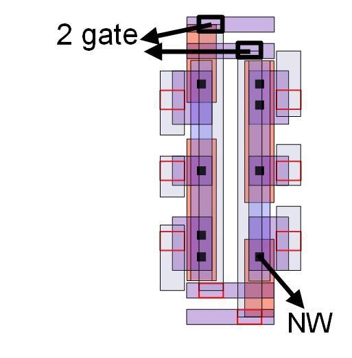
11 10nm 30nm 30nm 25nm 30nm 30nm 5nm 5nm 10nm 5nm From FinFET to lateral NW Fin 1 wire 2 wires 3 wires SiO 2 0.5nm Decrease Sswing & DIBL Fin HfO 2 1.5nm NW spacin g 5nm Roundin g radius 2.5nm Fin Increase R access Spacin g 5nm STI STI STI STI Higher stack is needed for nanowire FETs to compensate smaller cross section than FinFET. Increased parasitics require the enabling of new features e.g. internal spacers
12 Dynamic power [ W] Power-performance scaling: from FinFET to lateral NW nm 0.9V 14nm 9T FinFET 10nm 9T FinFET 0.8V 0.75V 10nm 7.5T FinFET 0.75V 7nm 7.5T NanoWire 0.7V RO INVD1 FO3 50 CGP BEOL load psige(50%), nsi 0.65V 0.45V 0.45V 0.55V 0.50V 0.50V 0.45V Performance [GHz] >50% +30% 5nm 7.5T NanoWire 0.65V 5nm 6T NanoWire 0.65V NW device allows further voltage scaling and performance gains


 Si/SiGe")

 Spacer, S/D,")
 SiGe")
13 Lateral NW: an evolutionary path from FinFET H. Mertens et al., VLSI Symp (a) Si/SiGe Multi-stack (b) Fin patterning & STI (c) Dummy gate (d) Spacer, S/D, ILD0 & Gate removal (e) SiGe or Si removal (f) Final gate stack


14 Demonstration of a 2-stacked lateral nanowire device H. Mertens et al., VLSI Symp No stressors WF metal 45nm Si NW RMG-HK 8 nm Demonstrated 2-stacked Si NWFET Improved performance and electrostatics as compared to FinFETs


15 Going vertical Integration Device Circuit System InGaAs W top contact Gate Si
16 High mobility materials
17 Carrier Mobility (cm 2 /Vs) Why high mobility materials? Graphene 400x After R. Pillarisetty, Nature, InSb InAs 10-40x Ge 2-6x Si GaAs InP V dd limited < 0.5V? Energy Band Gap (ev) New Materials with Major Transport Enhancement over Si


18 Challenges for high mobility materials Fin Replacement/Wide field/srb Epi & Integration Junction engineering & contacting InGaAs Gate stack & Surface Passivation Defect & Phys. Metrology Device performance and scalability

 Local Device-level Virtual")

19 Challenges for epitaxial growth Global Wafer-level Stress-Relaxed Buffer Local Wide-Area Virtual Substrate (Wide-Trench ART) Local Device-level Virtual Substrate (Narrow Trench ART) Defect layer InP 500 nm Si Defect layer 300mm 0.5 m-500nm < 50nm


20 20 Ge FinFET using fin replacement technique FIN PITCH DOWN TO 45NM L. Witters et al., VLSI Symp nm
![Gm sat [ S/ m] High performance III-V devices on 300mm Si 3000 2500 Q=30 300mm](/docs-images/72/66826153/images/21-1.jpg "GAA Q=20 V DD =0.5V Rectangles: InAs Triangles: InGaAs Q=10 N. Waldron et al.")

21 Gm sat [ S/ m] High performance III-V devices on 300mm Si Q=30 300mm GAA Q=20 V DD =0.5V Rectangles: InAs Triangles: InGaAs Q=10 N. Waldron et al., IEDM, X. Zhou et al., VLSI QW FF FinFET 300mm GAA IIIVoI 500 vertical NW IIIVoI CELO SS sat [mv/dev] 300mm FinFET Q=5
22 Need for co-integration with Si Leakage Power N7 Si FinFET V dd = 0.7V 25% 29% N10 Si FinFET V dd =0.8V IIIV/Ge V dd = 0.7V Si-Ge-IIIV Co-integrated? High mobility channels offer more performance but leakage span limited Need Si-channel co-integration for SOC


23 What about 2D materials? Advantages: Expected reduced SCE No dangling bonds Large choice of materials and bandgaps Challenges: Large scale growth of MX2 Choice of MX2 material for NFET and PFET Gate stack Contacts
24 Heterogeneous integration with base CMOS 3-D Hetero-SOC Cu Interconnect (T~400 o C) Sequentially Processed Can the 2-D crystals be selectively grown between the interconnects? Or by transfer & bond? 2-D Crystal Devices Cu Interconnect (T~400 o C) Base CMOS Thermal budget of 2-D device processing is typically low-t, but material growth is still unclear
25 New switching mechanisms


26 Moving to tunnel FET ULTRA-LOW VOLTAGE APPLICATIONS
![BTBT generation (cm -3 s -1 ) 27 From group IV to III-V 10 34 10 32 10 30 10 28 10 26 10 24 10 22 BTBT Generation Rate (GR) InGaAs53 (dir) [1] Ge (dir) Ge (ind) Si (ind) <110> direction 0 0.5 1 1.](/docs-images/72/66826153/images/27-1.jpg "5 2 2.")
27 BTBT generation (cm -3 s -1 ) 27 From group IV to III-V BTBT Generation Rate (GR) InGaAs53 (dir) [1] Ge (dir) Ge (ind) Si (ind) <110> direction Electric field (MV/cm) Probability of tunneling is dependent on bandgap Si dir Ge dir SiGe30 dir Higher tunneling SiGe50 dirgeneration rate for low bandgap SiGe80 materials dir InGaAs dir Si ind Increased Ge performance ind expected for III-V SiGe30 ind SiGe50 ind SiGe80 ind Kao et al, TED 59(2), 292 (2012) & [1] Q. Smets et al, SSDM 2013
![I d (ua/um) I on [µa/µm] @ I off = 100 pa/µm III-V homojunction n-tfet process and device 10 10 1 1 10 10 0 0 10 10-1 -1 10 10-2 -2 10 10-3 -3 10 10-4 -4 10 10-5 -5 10 10-6 -6 A. Alian et al.](/docs-images/72/66826153/images/28-1.jpg ", IEDM, 2015. Vd= 200 mv 70% 53% 53%-shifted 0.0 0.0 0.2 0.2 0.4 0.4 0.6 0.6 0.8 0.8 1.0 1.0 V g (V) 100 10 1 0.1 Dewey et al., p.")
28 I d (ua/um) I on I off = 100 pa/µm III-V homojunction n-tfet process and device A. Alian et al., IEDM, Vd= 200 mv 70% 53% 53%-shifted V g (V) Dewey et al., p. 45, VLSI 2012 [11] [8] [4] [6] Noguchi et al [10] Tomioka et al., p.47, VLSI, 2012 homo-junction hetero-junction This work [7] [5] SS min [mv/dec] Significant boost with 8nm strained InGaAs (70% In) (quantum confinement & bandgap) Very low TAT observed SS less degraded by D it in TFET due to energy range for carrier exchange in TFET operations
= 5.43 5.65 6.06 5.45 6.1 5.87 5.65 6.48 Substrate 0.")

29 III-V Heterostructures Staggered and broken gap configurations Si InAs GaSb GaAs Ge GaP InP InSb E c GaAsSb In 0.53 Ga 0.47 As E v InGaAs GaSb 0.5 As 0.5 a(a)= Substrate % Lattice InP mismatch 4% Lattice mismatch S. El Kazzi et al., EUROMBE A. Verhulst et al., IEDM, Sb-based materials needed to allow best trade-off between performance & electrostatics


30 From 3D TFET to 2D TFET After Eli Yablonovitch 2012, UC Berkeley 3D-3D 2D-2D Soft Transition Abrupt Transition Steepness of the swing over a wide-vg range limited by 3-D DOS Investigate 2-D TFET options


31 2-D TFETS with 2-D MX 2 (TMD) heterostructures DFT V G V S MoS 2 V G 0 V HfS 2 Left Device model electrode V D doped e /cm 2 High-k intrinsi c High-k Broken gap devices with large bandgaps 2nm Lattice mismatch is no longer an issue van der Waals stacking Right electrod e doped e /cm 2 31
 Tunable hysteresis behavior:")
32 Negative capacitance FET (NC-FET) SS= VGS s s (logid) = m x n S. Salahuddin et al., Nano letters, V G C FE s C S Sub 60mV/dec due to negative capacitance of a ferroelectric oxide based gate stack (m < 1) Tunable hysteresis behavior: non-volatile circuits and noise immune logic


33 Spin logic Spin based devices offer different Energy-Delay tradeoffs Spin torque majority gate D. Nikonov et al., IEEE EDL, Spin wave devices
34 Summary
35 Summary Need for more energy-efficient Core Logic Devices and specialty devices Lateral NW is a natural evolution from FinFET and will enable to continue scaling beyond 7nm due to improved electrostatics VFET offers 30-40% SRAM area benefit: 1 st step towards vertical logic? Scaling of supply voltage is required to address power crisis and higher mobility channels are needed to increase performance at reduced V DD New switching mechanisms like TFET, NCFET and spin logic being considered for ultra-low power applications
Integration of III-V heterostructure tunnel FETs on Si using Template Assisted Selective Epitaxy (TASE)
") Integration of III-V heterostructure tunnel FETs on Si using Template Assisted Selective Epitaxy (TASE) K. Moselund 1, D. Cutaia 1. M. Borg 1, H. Schmid 1, S. Sant 2, A. Schenk 2 and H. Riel 1 1 IBM Research
Integration of III-V heterostructure tunnel FETs on Si using Template Assisted Selective Epitaxy (TASE) K. Moselund 1, D. Cutaia 1. M. Borg 1, H. Schmid 1, S. Sant 2, A. Schenk 2 and H. Riel 1 1 IBM Research
Nanoscale III-V CMOS
 Nanoscale III-V CMOS J. A. del Alamo Microsystems Technology Laboratories Massachusetts Institute of Technology SEMI Advanced Semiconductor Manufacturing Conference Saratoga Springs, NY; May 16-19, 2016
Record I on (0.50 ma/μm at V DD = 0.5 V and I off = 100 na/μm) 25 nm-gate-length ZrO 2 /InAs/InAlAs MOSFETs
 25 nm-gate-length ZrO 2 /InAs/InAlAs MOSFETs") Record I on (0.50 ma/μm at V DD = 0.5 V and I off = 100 na/μm) 25 nm-gate-length ZrO 2 /InAs/InAlAs MOSFETs Sanghoon Lee 1*, V. Chobpattana 2,C.-Y. Huang 1, B. J. Thibeault 1, W. Mitchell 1, S. Stemmer
Record I on (0.50 ma/μm at V DD = 0.5 V and I off = 100 na/μm) 25 nm-gate-length ZrO 2 /InAs/InAlAs MOSFETs Sanghoon Lee 1*, V. Chobpattana 2,C.-Y. Huang 1, B. J. Thibeault 1, W. Mitchell 1, S. Stemmer
III-V CMOS: Quo Vadis?
 III-V CMOS: Quo Vadis? J. A. del Alamo, X. Cai, W. Lu, A. Vardi, and X. Zhao Microsystems Technology Laboratories Massachusetts Institute of Technology Compound Semiconductor Week 2018 Cambridge, MA, May
Enabling Breakthroughs In Technology
 Enabling Breakthroughs In Technology Mike Mayberry Director of Components Research VP, Technology and Manufacturing Group Intel Corporation June 2011 Defined To be defined Enabling a Steady Technology
Nanoscale III-V Electronics: from Quantum-Well Planar MOSFETs to Vertical Nanowire MOSFETs
 Nanoscale III-V Electronics: from Quantum-Well Planar MOSFETs to Vertical Nanowire MOSFETs J. A. del Alamo Microsystems Technology Laboratories, MIT Purdue University, West Lafayette, IN; September 29,
Innovation to Advance Moore s Law Requires Core Technology Revolution
 Innovation to Advance Moore s Law Requires Core Technology Revolution Klaus Schuegraf, Ph.D. Chief Technology Officer Silicon Systems Group Applied Materials UC Berkeley Seminar March 9 th, 2012 Innovation
III-V CMOS: the key to sub-10 nm electronics?
 III-V CMOS: the key to sub-10 nm electronics? J. A. del Alamo Microsystems Technology Laboratories, MIT 2011 MRS Spring Meeting and Exhibition Symposium P: Interface Engineering for Post-CMOS Emerging
HOW TO CONTINUE COST SCALING. Hans Lebon
 HOW TO CONTINUE COST SCALING Hans Lebon OUTLINE Scaling & Scaling Challenges Imec Technology Roadmap Wafer size scaling : 450 mm 2 COST SCALING IMPROVED PERFORMANCE 3 GLOBAL TRAFFIC FORECAST Cloud Traffic
III-V Vertical Nanowire FETs with Steep Subthreshold Towards Sub-10 nm Diameter Devices
 III-V Vertical Nanowire FETs with Steep Subthreshold Towards Sub-10 nm Diameter Devices Jesús A. del Alamo, Xin Zhao, Wenjie Lu, Alon Vardi Microsystems Technology Laboratories, MIT E 3 S Retreat September
InAs Quantum-Well MOSFET for logic and microwave applications
 AWAD June 29 th 2012 Accelerating the next technology revolution InAs Quantum-Well MOSFET for logic and microwave applications T.-W. Kim, R. Hill, C. D. Young, D. Veksler, L. Morassi, S. Oktybrshky 1,
Advanced PDK and Technologies accessible through ASCENT
 Advanced PDK and Technologies accessible through ASCENT MOS-AK Dresden, Sept. 3, 2018 L. Perniola*, O. Rozeau*, O. Faynot*, T. Poiroux*, P. Roseingrave^ olivier.faynot@cea.fr *Cea-Leti, Grenoble France;
III-V Channel Transistors
 III-V Channel Transistors Jesús A. del Alamo Professor Microsystems Technology Laboratories MIT Acknowledgements: Students and collaborators: D. Antoniadis, J. Lin, W. Lu, A. Vardi, X. Zhao Sponsors: Applied
Tunneling Field Effect Transistors for Low Power ULSI
 Tunneling Field Effect Transistors for Low Power ULSI Byung-Gook Park Inter-university Semiconductor Research Center and School of Electrical and Computer Engineering Seoul National University Outline
CMOS Scaling Beyond FinFETs: Nanowires and TFETs
 SEMATECH Symposium June 23, 2011 Tokyo Accelerating the next technology revolution CMOS Scaling Beyond FinFETs: Nanowires and TFETs Chris Hobbs, Wei-Yip Loh, Kerem Akarvardar, Paul Kirsch, and Raj Jammy
FinFET Devices and Technologies
 FinFET Devices and Technologies Jack C. Lee The University of Texas at Austin NCCAVS PAG Seminar 9/25/14 Material Opportunities for Semiconductors 1 Why FinFETs? Planar MOSFETs cannot scale beyond 22nm
Advanced Digital Integrated Circuits. Lecture 2: Scaling Trends. Announcements. No office hour next Monday. Extra office hour Tuesday 2-3pm
 EE241 - Spring 20 Advanced Digital Integrated Circuits Lecture 2: Scaling Trends and Features of Modern Technologies Announcements No office hour next Monday Extra office hour Tuesday 2-3pm 2 1 Outline
III-V on Si for VLSI. 200 mm III-V on Si. Accelerating the next technology revolution. III-V nfet on 200 mm Si
 III-V on Si for VLSI Accelerating the next technology revolution 200 mm III-V on Si III-V nfet on 200 mm Si R. Hill, C. Park, J. Barnett, J. Huang, N. Goel, J. Oh, W.Y. Loh, J. Price, P. Kirsch, P, Majhi,
Fin-Shaped Field Effect Transistor (FinFET) Min Ku Kim 03/07/2018
 Min Ku Kim 03/07/2018") Fin-Shaped Field Effect Transistor (FinFET) Min Ku Kim 03/07/2018 ECE 658 Sp 2018 Semiconductor Materials and Device Characterizations OUTLINE Background FinFET Future Roadmap Keeping up w/ Moore s Law
Fin-Shaped Field Effect Transistor (FinFET) Min Ku Kim 03/07/2018 ECE 658 Sp 2018 Semiconductor Materials and Device Characterizations OUTLINE Background FinFET Future Roadmap Keeping up w/ Moore s Law
InGaAs Nanoelectronics: from THz to CMOS
 InGaAs Nanoelectronics: from THz to CMOS J. A. del Alamo Microsystems Technology Laboratories, MIT IEEE International Conference on Electron Devices and Solid-State Circuits Hong Kong, June 3, 2013 Acknowledgements:
A New Self-aligned Quantum-Well MOSFET Architecture Fabricated by a Scalable Tight-Pitch Process
 A New Self-aligned Quantum-Well MOSFET Architecture Fabricated by a Scalable Tight-Pitch Process Jianqiang Lin, Xin Zhao, Tao Yu, Dimitri A. Antoniadis, and Jesús A. del Alamo Microsystems Technology Laboratories,
Towards Sub-10 nm Diameter InGaAs Vertical nanowire MOSFETs and TFETs
 Towards Sub-10 nm Diameter InGaAs Vertical nanowire MOSFETs and TFETs J. A. del Alamo, X. Zhao, W. Lu, and A. Vardi Microsystems Technology Laboratories Massachusetts Institute of Technology 5 th Berkeley
Zota, Cezar B.; Lindelow, Fredrik; Wernersson, Lars Erik; Lind, Erik
 InGaAs tri-gate MOSFETs with record on-current Zota, Cezar B.; Lindelow, Fredrik; Wernersson, Lars Erik; Lind, Erik Published in: 6 IEEE International Electron Devices Meeting, IEDM 6 DOI:.9/IEDM.6.7886
Beyond Transistor Scaling: New Devices for Ultra Low Energy Information Processing
 Beyond Transistor Scaling: New Devices for Ultra Low Energy Information Processing Prof. Tsu Jae King Liu Department of Electrical Engineering and Computer Sciences University of California, Berkeley,
Vertical InAs/GaAsSb/GaSb tunneling field-effect transistor on Si with S = 48 mv/decade and Ion = 10 A/m for Ioff = 1 na/m at VDS = 0.
 Vertical InAs/GaAsSb/GaSb tunneling field-effect transistor on Si with S = 48 mv/decade and Ion = 10 A/m for Ioff = 1 na/m at VDS = 0.3 V Memisevic, E.; Svensson, Johannes; Hellenbrand, Markus; Lind, Erik;
InGaAs MOSFET Electronics
 InGaAs MOSFET Electronics J. A. del Alamo Microsystems Technology Laboratories, MIT The 17 th International Symposium Physics of Semiconductors and Applications Jeju, Korea, December 7-11, 2014 Acknowledgements:
Transistor Scaling in the Innovation Era. Mark Bohr Intel Senior Fellow Logic Technology Development August 15, 2011
 Transistor Scaling in the Innovation Era Mark Bohr Intel Senior Fellow Logic Technology Development August 15, 2011 MOSFET Scaling Device or Circuit Parameter Scaling Factor Device dimension tox, L, W
32nm Technology and Beyond
 32nm Technology and Beyond Paolo Gargini Chairman ITRS IEEE Fellow Director of Technology Strategy Intel Fellow ISS Europe 2009 P. Gargini 1 Agenda Equivalent Scaling 45nm Technology summary 32nm Technology
Nanometer-Scale InGaAs Field-Effect Transistors for THz and CMOS Technologies
 Nanometer-Scale InGaAs Field-Effect Transistors for THz and CMOS Technologies J. A. del Alamo Microsystems Technology Laboratories, MIT ESSDERC-ESSCIRC 2013 Bucharest, Romania, September 16-20, 2013 Acknowledgements:
Challenges and Innovations in Nano CMOS Transistor Scaling
 Challenges and Innovations in Nano CMOS Transistor Scaling Tahir Ghani Intel Fellow Logic Technology Development October, 2009 Nikkei Presentation 1 Outline Traditional Scaling Traditional Scaling Limiters,
FinFET-based Design for Robust Nanoscale SRAM
 FinFET-based Design for Robust Nanoscale SRAM Prof. Tsu-Jae King Liu Dept. of Electrical Engineering and Computer Sciences University of California at Berkeley Acknowledgements Prof. Bora Nikoli Zheng
Sustaining the Si Revolution: From 3D Transistors to 3D Integration
 Sustaining the Si Revolution: From 3D Transistors to 3D Integration Tsu Jae King Liu Department of Electrical Engineering and Computer Sciences University of California, Berkeley, CA USA February 23, 2015
ITRS MOSFET Scaling Trends, Challenges, and Key Technology Innovations
 Workshop on Frontiers of Extreme Computing Santa Cruz, CA October 24, 2005 ITRS MOSFET Scaling Trends, Challenges, and Key Technology Innovations Peter M. Zeitzoff Outline Introduction MOSFET scaling and
Fully Depleted Devices
 4 Fully Depleted Devices FDSOI and FinFET Bruce Doris, Ali Khakifirooz, Kangguo Cheng, and Terence Hook CONTENTS 4.1 Overview... 71 4.2 Introduction: Challenges of Conventional CMOS Technology...72 4.3
SoC Technology in the Era of 3-D Tri-Gate Transistors for Low Power, High Performance, and High Density Applications
 SoC Technology in the Era of 3-D Tri-Gate Transistors for Low Power, High Performance, and High Density Applications Vice President, Technology Manufacturing Group Intel Corporation August 2013 Outlines
Atomic-layer deposition of ultrathin gate dielectrics and Si new functional devices
 Atomic-layer deposition of ultrathin gate dielectrics and Si new functional devices Anri Nakajima Research Center for Nanodevices and Systems, Hiroshima University 1-4-2 Kagamiyama, Higashi-Hiroshima,
Record Extrinsic Transconductance (2.45 ms/μm at V DS = 0.5 V) InAs/In 0.53 Ga 0.47 As Channel MOSFETs Using MOCVD Source-Drain Regrowth
 InAs/In 0.53 Ga 0.47 As Channel MOSFETs Using MOCVD Source-Drain Regrowth") Record Extrinsic Transconductance (2.45 ms/μm at = 0.5 V) InAs/In 0.53 Ga 7 As Channel MOSFETs Using MOCVD Source-Drain Regrowth Sanghoon Lee 1*, C.-Y. Huang 1, A. D. Carter 1, D. C. Elias 1, J. J. M.
Record Extrinsic Transconductance (2.45 ms/μm at = 0.5 V) InAs/In 0.53 Ga 7 As Channel MOSFETs Using MOCVD Source-Drain Regrowth Sanghoon Lee 1*, C.-Y. Huang 1, A. D. Carter 1, D. C. Elias 1, J. J. M.
In principle, the high mobilities of InGaAs and
 114Conference report: IEDM part 2 Meeting the challenge of integrating III-Vs with deep submicron silicon High-mobility devices based on indium gallium arsenide (InGaAs) channels could benefit the performance
Alternative Channel Materials for MOSFET Scaling Below 10nm
 Alternative Channel Materials for MOSFET Scaling Below 10nm Doug Barlage Electrical Requirements of Channel Mark Johnson Challenges With Material Synthesis Introduction Outline Challenges with scaling
FinFET vs. FD-SOI Key Advantages & Disadvantages
 FinFET vs. FD-SOI Key Advantages & Disadvantages Amiad Conley Technical Marketing Manager Process Diagnostics & Control, Applied Materials ChipEx-2014, Apr 2014 1 Moore s Law The number of transistors
45nm Bulk CMOS Within-Die Variations. Courtesy of C. Spanos (UC Berkeley) Lecture 11. Process-induced Variability I: Random
 Lecture 11. Process-induced Variability I: Random") 45nm Bulk CMOS Within-Die Variations. Courtesy of C. Spanos (UC Berkeley) Lecture 11 Process-induced Variability I: Random Random Variability Sources and Characterization Comparisons of Different MOSFET
45nm Bulk CMOS Within-Die Variations. Courtesy of C. Spanos (UC Berkeley) Lecture 11 Process-induced Variability I: Random Random Variability Sources and Characterization Comparisons of Different MOSFET
InGaAs MOSFETs for CMOS:
 InGaAs MOSFETs for CMOS: Recent Advances in Process Technology J. A. del Alamo, D. Antoniadis, A. Guo, D.-H. Kim 1, T.-W. Kim 2, J. Lin, W. Lu, A. Vardi and X. Zhao Microsystems Technology Laboratories,
Parameter Optimization Of GAA Nano Wire FET Using Taguchi Method
 Parameter Optimization Of GAA Nano Wire FET Using Taguchi Method S.P. Venu Madhava Rao E.V.L.N Rangacharyulu K.Lal Kishore Professor, SNIST Professor, PSMCET Registrar, JNTUH Abstract As the process technology
ECE 5745 Complex Digital ASIC Design Topic 2: CMOS Devices
 ECE 5745 Complex Digital ASIC Design Topic 2: CMOS Devices Christopher Batten School of Electrical and Computer Engineering Cornell University http://www.csl.cornell.edu/courses/ece5950 Simple Transistor
Near/Mid-Infrared Heterogeneous Si Photonics
 PHOTONICS RESEARCH GROUP Near/Mid-Infrared Heterogeneous Si Photonics Zhechao Wang, PhD Photonics Research Group Ghent University / imec, Belgium ICSI-9, Montreal PHOTONICS RESEARCH GROUP 1 Outline Ge-on-Si
EE241 - Spring 2013 Advanced Digital Integrated Circuits. Announcements. Sign up for Piazza if you haven t already
 EE241 - Spring 2013 Advanced Digital Integrated Circuits Lecture 2: Scaling Trends and Features of Modern Technologies Announcements Sign up for Piazza if you haven t already 2 1 Assigned Reading R.H.
Experimentally reported sub-60mv/dec
 Experimentally reported sub-60mv/dec swing in Tunnel FETs? 1 We considered InAs conventional, lateral transistor architectures: GAA nanowire, Fin FETs FETs (Tri gate) UTB,DG SOI Analysis is not directly
Sub-micron technology IC fabrication process trends SOI technology. Development of CMOS technology. Technology problems due to scaling
 Goodbye Microelectronics Welcome Nanoelectronics Sub-micron technology IC fabrication process trends SOI technology SiGe Tranzistor in 50nm process Virus The thickness of gate oxide= 1.2 nm!!! Today we
Vertical Nanowire InGaAs MOSFETs Fabricated by a Top-down Approach
 Vertical Nanowire InGaAs MOSFETs Fabricated by a Top-down Approach Xin Zhao, Jianqiang Lin, Christopher Heidelberger, Eugene A. Fitzgerald and Jesús A. del Alamo Microsystems Technology Laboratories, MIT
ATV 2011: Computer Engineering
 ATV 2011: Technology Trends in Computer Engineering Professor Per Larsson-Edefors ATV 2011, L1, Per Larsson-Edefors Page 1 Solid-State Devices www.cse.chalmers.se/~perla/ugrad/ SemTech/Lectures_2000.pdf
Alternatives to standard MOSFETs. What problems are we really trying to solve?
 Alternatives to standard MOSFETs A number of alternative FET schemes have been proposed, with an eye toward scaling up to the 10 nm node. Modifications to the standard MOSFET include: Silicon-in-insulator
450mm and Moore s Law Advanced Packaging Challenges and the Impact of 3D
 450mm and Moore s Law Advanced Packaging Challenges and the Impact of 3D Doug Anberg VP, Technical Marketing Ultratech SOKUDO Lithography Breakfast Forum July 10, 2013 Agenda Next Generation Technology
Research Needs for Device Sciences Modeling and Simulation (May 6, 2005)
") Research Needs for Device Sciences Modeling and Simulation (May 6, 2005) SRC Device Sciences 2005 Modeling and Simulation Task Force Contributing organizations: Axcelis, Freescale, IBM, Intel, LSI, SRC,
Research Needs for Device Sciences Modeling and Simulation (May 6, 2005) SRC Device Sciences 2005 Modeling and Simulation Task Force Contributing organizations: Axcelis, Freescale, IBM, Intel, LSI, SRC,
Lecture: Integration of silicon photonics with electronics. Prepared by Jean-Marc FEDELI CEA-LETI
 Lecture: Integration of silicon photonics with electronics Prepared by Jean-Marc FEDELI CEA-LETI Context The goal is to give optical functionalities to electronics integrated circuit (EIC) The objectives
Sub-30 nm InAs Quantum-Well MOSFETs with Self-Aligned Metal Contacts and Sub-1 nm EOT HfO 2 Insulator
 Sub-30 nm InAs Quantum-Well MOSFETs with Self-Aligned Metal Contacts and Sub-1 nm EOT HfO 2 Insulator Jianqiang Lin, Dimitri A. Antoniadis, and Jesús A. del Alamo Microsystems Technology Laboratories,
Introducing 7-nm FinFET technology in Microwind
 Introducing 7-nm FinFET technology in Microwind Etienne SICARD Professor INSA-Dgei, 135 Av de Rangueil 31077 Toulouse France www.microwind.org email: Etienne.sicard@insa-toulouse.fr This paper describes
High-Performance Si Nanowire FET with a Semi Gate-Around Structure Suitable for Integration
 High-Performance Si Nanowire FET with a Semi Gate-Around Structure Suitable for Integration Soshi Sato 1, Hideyuki Kamimura 1, Hideaki Arai 1, Kuniyuki Kakushima 2, Parhat Ahmet 1, Kenji Ohmori 3, Keisaku
SiNANO-NEREID Workshop:
 SiNANO-NEREID Workshop: Towards a new NanoElectronics Roadmap for Europe Leuven, September 11 th, 2017 WP3/Task 3.1: Nanoscale FET Anda Mocuta Introduction: technologies/concepts covered by the Roadmap
Lecture 33 - The Short Metal-Oxide-Semiconductor Field-Effect Transistor (cont.) April 30, 2007
 April 30, 2007") 6.720J/3.43J - Integrated Microelectronic Devices - Spring 2007 Lecture 33-1 Lecture 33 - The Short Metal-Oxide-Semiconductor Field-Effect Transistor (cont.) April 30, 2007 Contents: 1. MOSFET scaling
6.720J/3.43J - Integrated Microelectronic Devices - Spring 2007 Lecture 33-1 Lecture 33 - The Short Metal-Oxide-Semiconductor Field-Effect Transistor (cont.) April 30, 2007 Contents: 1. MOSFET scaling
Enabling Power-Efficient Designs With III-V Heterojunction Tunnel FETs
 Enabling Power-Efficient Designs With III-V Heterojunction Tunnel FETs Moon S. Kim, Huichu Liu, Karthik Swaminathan, Xueqing Li, Suman Datta, and Vijaykrishnan Narayanan The Pennsylvania State University
Comparative Study of Silicon and Germanium Doping-less Tunnel Field Effect Transistors
 IJSTE - International Journal of Science Technology & Engineering Volume 2 Issue 5 November 2015 ISSN (online): 2349-784X Comparative Study of Silicon and Germanium Doping-less Tunnel Field Effect Transistors
Chapter 3: Basics Semiconductor Devices and Processing 2006/9/27 1. Topics
 Chapter 3: Basics Semiconductor Devices and Processing 2006/9/27 1 Topics What is semiconductor Basic semiconductor devices Basics of IC processing CMOS technologies 2006/9/27 2 1 What is Semiconductor
Session 3: Solid State Devices. Silicon on Insulator
 Session 3: Solid State Devices Silicon on Insulator 1 Outline A B C D E F G H I J 2 Outline Ref: Taurand Ning 3 SOI Technology SOl materials: SIMOX, BESOl, and Smart Cut SIMOX : Synthesis by IMplanted
Active Technology for Communication Circuits
 EECS 242: Active Technology for Communication Circuits UC Berkeley EECS 242 Copyright Prof. Ali M Niknejad Outline Comparison of technology choices for communication circuits Si npn, Si NMOS, SiGe HBT,
General look back at MESFET processing. General principles of heterostructure use in FETs
 SMA5111 - Compound Semiconductors Lecture 11 - Heterojunction FETs - General HJFETs, HFETs Last items from Lec. 10 Depletion mode vs enhancement mode logic Complementary FET logic (none exists, or is likely
Design of Tunnel FET and its Performance characteristics with various materials
 Design of Tunnel FET and its Performance characteristics with various materials 1 G.SANKARAIAH, 2 CH.SATHYANARAYANA 1 PG Student Sreenidhi Institute of Science and Technology, 2 Assistant Professor 1,
Semiconductor Memory: DRAM and SRAM. Department of Electrical and Computer Engineering, National University of Singapore
 Semiconductor Memory: DRAM and SRAM Outline Introduction Random Access Memory (RAM) DRAM SRAM Non-volatile memory UV EPROM EEPROM Flash memory SONOS memory QD memory Introduction Slow memories Magnetic
SUPPLEMENTARY INFORMATION
 SUPPLEMENTARY INFORMATION doi:10.1038/nature11293 1. Formation of (111)B polar surface on Si(111) for selective-area growth of InGaAs nanowires on Si. Conventional III-V nanowires (NWs) tend to grow in
FinFETs have emerged as the solution to short channel
 IEEE TRANSACTIONS ON ELECTRON DEVICES 1 Fin Shape Impact on FinFET Leakage With Application to Multithreshold and Ultralow-Leakage FinFET Design Brad D. Gaynor and Soha Hassoun, Senior Member, IEEE Abstract
Transistors for VLSI, for Wireless: A View Forwards Through Fog
 Plenary, Device Research Conference, June 22, 2015, Ohio State Transistors for VLSI, for Wireless: A View Forwards Through Fog Mark Rodwell, UCSB Low-voltage devices P. Long, E. Wilson, S. Mehrotra, M.
EECS130 Integrated Circuit Devices
 EECS130 Integrated Circuit Devices Professor Ali Javey 11/6/2007 MOSFETs Lecture 6 BJTs- Lecture 1 Reading Assignment: Chapter 10 More Scalable Device Structures Vertical Scaling is important. For example,
POST CMOS PATHFINDING. Leti Innovation Days June 28-29, 2017
 POST CMOS PATHFINDING DEVELOPING THE BUILDING BLOCKS FOR DATA PROCESSING The challenges to continue the performance improvement of data processing systems are multiple Improve the energy efficiency to
Chapter 3 Basics Semiconductor Devices and Processing
 Chapter 3 Basics Semiconductor Devices and Processing 1 Objectives Identify at least two semiconductor materials from the periodic table of elements List n-type and p-type dopants Describe a diode and
Scaling of Vertical InAs GaSb Nanowire Tunneling Field-Effect Transistors on Si
 Scaling of Vertical InAs GaSb Nanowire Tunneling Field-Effect Transistors on Si Memisevic, Elvedin; Svensson, Johannes; Hellenbrand, Markus; Lind, Erik; Wernersson, Lars-Erik Published in: IEEE Electron
Past and future for micro- and nano-electronics, focusing on Si integrated circuits technology
 Past and future for micro- and nano-electronics, focusing on Si integrated circuits technology June 2, 2008 @National Technical University of Athens Hiroshi Iwai, Toyo Institute of Technology Needless
Thermal Management in the 3D-SiP World of the Future
 Thermal Management in the 3D-SiP World of the Future Presented by W. R. Bottoms March 181 th, 2013 Smaller, More Powerful Portable Devices Are Driving Up Power Density Power (both power delivery and power
EE E6930 Advanced Digital Integrated Circuits. Spring, 2002 Lecture 12. SOI Devices and Circuits
 EE E6930 Advanced Digital Integrated Circuits Spring, 2002 Lecture 12. SOI Devices and Circuits References CBF, Chapter 5 On-line course reader on SOI Many slides borrowed from C. T. Chuang s 2001 tutorial
SOI technology platforms for 5G: Opportunities of collaboration
 SOI technology platforms for 5G: Opportunities of collaboration Dr. Ionut RADU Director, R&D SOITEC MOS AK workshop, Silicon Valley December 6th, 2017 Sourcing value from substrate Robert E. White ISBN-13:
Nanowire Tunnel Field Effect Transistors at High Temperature
 Nanowire Tunnel Field Effect Transistors at High Temperature Márcio D. V. Martino 1, Felipe S. Neves 1, Paula G. D. Agopian 1, João A. Martino 1, Rita Rooyackers 2 and Cor Claeys 2,3 1 LSI / PSI / USP
シリコン集積回路の現状と その微細化終焉後の世界 平成 20 年度 飯綱 サイエンスサマー道場 進化 発展するナノエレクトロニクス その本命は? 2008 年 8 月 19 日 長野県飯綱高原 ホテルアルカディア 東京工業大学 岩井 洋 1
 20? 2008 8 19 1 Si CMOS CMOS,,,,,,, CMOS 2 3 1960 IC (Integrated Circuits) ~ 10 1970 LSI (Large Scale Integrated Circuit) ~1,000 1980 VLSI (Very Large Scale IC) ~10,000 1990 ULSI (Ultra Large Scale IC)
Performance Analysis of InGaAs Double Gate MOSFET
 Performance Analysis of InGaAs Double Gate MOSFET Ms. Karthika Rani P, Ms. Kavitha T Abstract-Technological improvements have been made due to the scaling of device dimensions in order to attain continuous
Scaling of InGaAs MOSFETs into deep-submicron regime (invited)
") Scaling of InGaAs MOSFETs into deep-submicron regime (invited) Y.Q. Wu, J.J. Gu, and P.D. Ye * School of Electrical and Computer Engineering, Purdue University, West Lafayette, IN 47906 * Tel: 765-494-7611,
Scaling of InGaAs MOSFETs into deep-submicron regime (invited) Y.Q. Wu, J.J. Gu, and P.D. Ye * School of Electrical and Computer Engineering, Purdue University, West Lafayette, IN 47906 * Tel: 765-494-7611,
EECS130 Integrated Circuit Devices
 EECS130 Integrated Circuit Devices Professor Ali Javey 11/01/2007 MOSFETs Lecture 5 Announcements HW7 set is due now HW8 is assigned, but will not be collected/graded. MOSFET Technology Scaling Technology
A 90 nm High Volume Manufacturing Logic Technology Featuring Novel 45 nm Gate Length Strained Silicon CMOS Transistors
 A 90 nm High Volume Manufacturing Logic Technology Featuring Novel 45 nm Gate Length Strained Silicon CMOS Transistors T. Ghani, M. Armstrong, C. Auth, M. Bost, P. Charvat, G. Glass, T. Hoffmann*, K. Johnson#,
Lecture #29. Moore s Law
 Lecture #29 ANNOUNCEMENTS HW#15 will be for extra credit Quiz #6 (Thursday 5/8) will include MOSFET C-V No late Projects will be accepted after Thursday 5/8 The last Coffee Hour will be held this Thursday
Self-aligned, gate-last process for vertical InAs nanowire MOSFETs on Si
 Self-aligned, gate-last process for vertical InAs nanowire MOSFETs on Si Berg, Martin; Persson, Karl-Magnus; Kilpi, Olli-Pekka; Svensson, Johannes; Lind, Erik; Wernersson, Lars-Erik Published in: Technical
The 3 D Tri Gate transistor is a variant of the FinFET developed at UC Berkeley, and is being used in Intel s 22nmgeneration. microprocessors.
 On May 4, 2011, Intel Corporation announced what it called the most radical shift in semiconductor technology in 50 years. A new 3 dimensional transistor design will enable the production of integrated
Session 10: Solid State Physics MOSFET
 Session 10: Solid State Physics MOSFET 1 Outline A B C D E F G H I J 2 MOSCap MOSFET Metal-Oxide-Semiconductor Field-Effect Transistor: Al (metal) SiO2 (oxide) High k ~0.1 ~5 A SiO2 A n+ n+ p-type Si (bulk)
3-D Modelling of the Novel Nanoscale Screen-Grid Field Effect Transistor (SGFET)
") 3-D Modelling of the Novel Nanoscale Screen-Grid Field Effect Transistor (SGFET) Pei W. Ding, Kristel Fobelets Department of Electrical Engineering, Imperial College London, U.K. J. E. Velazquez-Perez
3-D Modelling of the Novel Nanoscale Screen-Grid Field Effect Transistor (SGFET) Pei W. Ding, Kristel Fobelets Department of Electrical Engineering, Imperial College London, U.K. J. E. Velazquez-Perez
Quantum-effect Resonant Tunneling Device Technology for Practical Ultra Low-power High-speed Applications
 Quantum-effect Resonant Tunneling Device Technology for Practical Ultra Low-power High-speed Applications SEMATECH Symposium October 23 rd, 2012 Prof. Kyounghoon Yang High Speed Nanoelectronics Laboratory
Study of Pattern Area of Logic Circuit. with Tunneling Field-Effect Transistors
 Contemporary Engineering Sciences, Vol. 6, 2013, no. 6, 273-284 HIKARI Ltd, www.m-hikari.com http://dx.doi.org/10.12988/ces.2013.3632 Study of Pattern Area of Logic Circuit with Tunneling Field-Effect
Scaling Electronics: Kelin J. Kuhn Intel Fellow. Kelin Kuhn / MIT / April 4 th
 Scaling Electronics: Trends and Bottlenecks Kelin J. Kuhn Intel Fellow Director of Advanced Device Technology 1 Moore s Law Scaling of the SRAM 10.00 Bitcell Area ( m 2 ) 1.00 0.10 2X bitcell area scaling
Tunnel FETs trends and challenges
 Tunnel FETs trends and challenges NEREID Nanoscale FET Workshop Bertinoro, Oct. 2016 -NEREID H2020 ICT CSA- Francis Balestra IMEP-LAHC Grenoble INP-Minatec/CNRS Introduction: Challenges of nanodevices
MSE 410/ECE 340: Electrical Properties of Materials Fall 2016 Micron School of Materials Science and Engineering Boise State University
 MSE 410/ECE 340: Electrical Properties of Materials Fall 2016 Micron School of Materials Science and Engineering Boise State University Practice Final Exam 1 Read the questions carefully Label all figures
EECS 151/251A Spring 2019 Digital Design and Integrated Circuits. Instructors: Wawrzynek. Lecture 8 EE141
 EECS 151/251A Spring 2019 Digital Design and Integrated Circuits Instructors: Wawrzynek Lecture 8 EE141 From the Bottom Up IC processing CMOS Circuits (next lecture) EE141 2 Overview of Physical Implementations
NEXT GENERATION SILICON PHOTONICS FOR COMPUTING AND COMMUNICATION PHILIPPE ABSIL
 NEXT GENERATION SILICON PHOTONICS FOR COMPUTING AND COMMUNICATION PHILIPPE ABSIL OUTLINE Introduction Platform Overview Device Library Overview What s Next? Conclusion OUTLINE Introduction Platform Overview
Opportunities and Challenges for Nanoelectronic Devices and Processes
 The Sixth U.S.-Korea Forum on Nanotechnology, April 28-29, 2009, Las Vegas, NV Opportunities and Challenges for Nanoelectronic Devices and Processes Yoshio Nishi Professor, Electrical Engineering, Material
Chapter 1. Introduction
 Chapter 1 Introduction 1.1 Introduction of Device Technology Digital wireless communication system has become more and more popular in recent years due to its capability for both voice and data communication.
NW-NEMFET: Steep Subthreshold Nanowire Nanoelectromechanical Field-Effect Transistor
 NW-NEMFET: Steep Subthreshold Nanowire Nanoelectromechanical Field-Effect Transistor Jie Xiang Electrical and Computer Engineering and Materials Science Engineering University of California, San Diego
+1 (479)
") Introduction to VLSI Design http://csce.uark.edu +1 (479) 575-6043 yrpeng@uark.edu Invention of the Transistor Vacuum tubes ruled in first half of 20th century Large, expensive, power-hungry, unreliable
Introduction to VLSI Design http://csce.uark.edu +1 (479) 575-6043 yrpeng@uark.edu Invention of the Transistor Vacuum tubes ruled in first half of 20th century Large, expensive, power-hungry, unreliable