Scaling Electronics: Kelin J. Kuhn Intel Fellow. Kelin Kuhn / MIT / April 4 th
|
|
|
- Wesley McCarthy
- 5 years ago
- Views:
Transcription
1 Scaling Electronics: Trends and Bottlenecks Kelin J. Kuhn Intel Fellow Director of Advanced Device Technology 1
 1.00 0.")

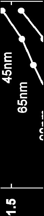
2 Moore s Law Scaling of the SRAM Bitcell Area ( m 2 ) X bitcell area scaling 90nm 65nm 45nm 32nm Process generation 22nm 2

")


3 Impact of Process Enhancers um) current (ma/u Drive S. Natarajan, IEDM 2008 S. Natarajan, IEDM


4 III-V MO OBILITY Source Gate n-ge Ge Drain System-in-package STRUCTURE Strain System-on-chip 32nm UTB SOI Fins Wires/Ribbons ELECTROSTATIC Kelin Kuhn / MIT / April 4CONFINEMENT th 2011
5 III-V MO OBILITY Source Gate n-ge Ge Drain System-in-package STRUCTURE Strain System-on-chip 32nm UTB SOI Fins Wires/Ribbons ELECTROSTATIC Kelin Kuhn / MIT / April 4CONFINEMENT th 2011
6 Transistor Performance Trend Drive Current (ma/um) V, 100 na I OFF 90nm 130nm 65nm 45nm 32nm Strain Hi-k-MG Other Classic scaling PMOS Gate Pitch (nm) 100 Strain is a critical ingredient in modern transistor scaling Strain was first introduced at 90nm, and its contribution has increased in each subsequent generation 6


7 Strain in modern devices Stress memorization Wei, VLSI 2007 Mayuzumi, IEDM 2007 Ghani, IEDM 2003 Yang, IEDM 2008 Auth, VLSI 2008
 <110>")
 Surface /")

 <110> Three possible channel")
8 ORIENTATION (100) surface top down (110) surface top down <110> <100> (100) <110> <110> Standard wafer / direction (100) Surface / <110> channel (100) Surface / <100> (a 45 degree wafer) Both <110> directions are the same. <100> Non-standard <111> (110) Surface (110) <110> Three possible channel directions <110> <111> and <100> <100>

9 ORIENTATION (100) surface top down (110) surface top down (100) <110> <100> <110> Standard wafer / direction (100) Surface / <110> channel (100) Surface / <100> (a 45 degree wafer) Both <110> directions are the same. (110) <100> <111> <110> Non-standard (110) Surface <110> <100> (100) BEST NMOS (110) <110> BEST PMOS Three possible channel directions <110> <111> and <100> Yang Yang AMD/IBM EDST EDST


10 Orientation and Strain: More complex for non-(100) orientations Modified from Thompson IEDM


11 Si vs Ge MOSFETs Gate Source Source n-ge Drain Intel 45nm HiK-MG Si device Intel HiK-MG Ge device The introduction of manufacturable HiK-MG transistors has led to the reconsideration of Ge channels 12
12 The image cannot be displayed. Your computer may not have enough memory to open the image, or the image may have been corrupted. Restart your computer, and then open the file again. If the red x still appears, you may have to delete the image and then insert it again. The image cannot be displayed. Your computer may not have enough memory to open the image, or the image may have been corrupted. Restart your computer, and then open the file again. If the red x still appears, you may have to delete the image and then insert it again. Challenge of Lattice Mismatch Issues Device Layer Silicon Direct Deposition Defects Si Silicon Dislocations III-V Stacking faults Si Twin Defects Adapted from J. Kavalieros VLSI SC
13 Ge and PMOS Bandgap and Electron Affinity (ev) Hole and Electron Mobility (cm2-v.s) 0 1 Si Ge InP GaAs InSb Ge mobility makes it uniquely interesting for PMOS K. Kuhn ECS
14 Low Field Long Channel Mobility (as a function of stress) 1000 Si (110) Si cm^2/vs Mobility (100) Si 200 Hole Stress (GPa) K. Kuhn ECS
15 Low Field Long Channel Mobility (as a function of stress) Si (100) Ge (110) Si Ge (110) Ge Mobility cm^2/vs (100) Si 200 Hole Stress (GPa) K. Kuhn ECS
16 Bandg gap and Ele ectron Affin nity (ev) Ge Historical Issues: Still critical today Si Ge InP GaAs InSb MO (cm2/v V.s) Si (no strain) Ge 100% Ge 55% SiGe 25% TOXE (A) Narrow Bandgap Poor Quality Dielectric K. Kuhn ECS
17 Narrow Bandgap Ene ergy Bandga ap (ev) Eg SiGe (PERCENTAGE) mobility (cm m^2/v.s) Hole s [A/um] Id, I Source 1.E-03 1.E-04 1.E-05 1.E-06 1.E-07 Adapted from Saraswat [59], Krishnamohan [60] BTBT h e DRAIN DRAIN High Junction Leakage Eg Drain 1.E-08 Source Source 1.E Vg - Vt [V] Band-to-band tunneling: challenge for low Eg materials K. Kuhn ECS
18 Narrow Bandgap Adapted from Saraswat [59], Krishnamohan [60] Source High BTBT Weak quantum confinement Narrow effective energy gap Source h e Eg Drain Reduced BTBT Strong quantum confinement Wide effective energy gap h e Eg Drain Two solutions: Use lower voltages and/or use quantum confined systems K. Kuhn ECS
19 Bandg gap and Ele ectron Affin nity (ev) Ge Historical Issues: Still critical today Si Ge InP GaAs InSb MO (cm2/v V.s) Si (no strain) Ge 100% Ge 55% SiGe 25% TOXE (A) Narrow Bandgap Poor Quality Dielectric K. Kuhn ECS
 Heynes,")
![2008 [9] Since HiK-MG dielectrics typically](/docs-images/82/85553940/images/20-1.jpg "form with a bilayer (the HiK + an interface")


20 Dielectric Quality Ge to GeO (110) 2 Ge/Ge GeO 2 sub oxide transition Ge(111) Heynes, 2008 [9] Since HiK-MG dielectrics typically form with a bilayer (the HiK + an interface layer) the challenge of germanium oxide still exists. Germanium oxide exists in several morphologies, unfortunately, most are hydroscopic and/or volatile. K. Kuhn ECS


21 Ge Dielectric: One strategy: Use an Si passivation layer Zimmerman IEDM 2006 Si passivation Hellings EDL 2009 Si passivation Mitard VLSI 2009 Si passivation 22


22 Ge Dielectric: Another strategy: Advanced GeO 2 processing Ge diffusion High-pressure O2 (HPO) suppresses surface reaction Low-T oxygen Annealing (LOA) Kita IEDM 2009 HPO + LOA Lee IEDM 2009 HPO + LOA Kuzum TED 2009 GeOxNy + LOA 23
23 Ge Benchmarking Yamamoto 2007 Wang 2007 Ioff (A/u um) Irisawa E-03 1.E-04 1.E-05 1.E-06 1.E-07 1E08 1.E-08 Romanjek 2008 Nicholas 2007 Batail 2009 Zimmerman 2006 Tezuka 2006 Andrieu E Liao 2008 Ion (ma/um) Harris 2007 Mitard 2009 Hellings 2009 Batail [2009] updated 24
24 III-V vs Ge: NMOS The Lure of High Mobility d y (ev) ndgap and n Affinity Ban Electro Si Ge InP GaAs InSb ron V.s) nd Electr ty (cm2-v Hole an Mobili Adapted from J. Kavalieros - VLSI SC 2007 K. Kuhn ECS
25 Low m* MOSFETs: Density-of-states states bottleneck On-current of a MOSFET I Q Velocity υ Diffusive : mobility μ, υ = μe Ballistic: injection velocity υ inj Light m* high μ, high υ inj From R. Kim Charge Q MOS limit (C Q» C ox ), C C ox Light m* less D (C Q ), less C, less Q More important for thin oxide (large C ox ), DOS bottleneck Q C V V G C C C C Q ox 2 q D Q th 26
26 T. Kelin Skotnicki, Kuhn / MIT IEDM / April th SC
27 Success of III-V Materials as Transistor sto Channel (Vcc = 0.5V) LECTRON MO OBILITY [cm 2 /V Vs] E Silicon InSb * InGaAs >30X improvement x x10 13 SHEET CARRIER DENSITY [cm -2 ] >5X R. Chau, Intel, ESSDERC 2008 At Vcc ~ 0.5V III-V n-channel devices show significantly higher mobility (30X) and higher effective velocity (5X) than strained silicon MOSFETs 28
28 Significant Gain in Intrinsic Drive Over Si at Low Vcc (e.g. 0.5V) Measurement Data 55% rrent, I (ma/ / m) D Drain cu Experiment & Simulation 80nm InGaAs QW, T OXE =27A R SD matched to Si (Simulated) 80nm InGaAs QW T OXE =34A 2X R SD 40nm Strained Si 20% 0.1 T OXE =14A V -V =0.3V G T Drain voltage, V (V) DS 80% R. Chau, ESSDERC 2008 At a gate overdrive = 0.3V, III-V QWFET shows 55% intrinsic drive current gain over strained Si At a drain voltage of 0.5V, III-V QWFET shows >20% I DSAT gain over strained Si (despite thicker Toxe and higher R SD) 29
29 5 High-Current L & -L channels: 5 Approaches Rodwell et al, 2010 Device Research Conference 6/21/2010 Rodwell, DRC, 2010 blue=occupied red=vacant ed drive current K 1 normaliz only InGaAs EET=Equivalent Electrostatic Thickness =T / +T / ox SiO2 ox inversion SiO2 semiconductor Si 0.4 nm 0.6 nm EET=1.0 nm g=2 g=1 0 includes the wavefunction depth term T inversion SiO2 / semiconductor m*/m o normalize ed drive current K nm EET=1.0 nm 0.3 nm 0.4 nm EET=Equivalent Electrostatic Thickness =T ox SiO2 / ox +T inversion SiO2 / semiconductor g=2, m /m =0.7 perpendicular 0 g=2, m /m =0.6 perpendicular 0 g=2, m perpendicular /m 0 =0.5 ma V 1 84 gs V J K th m 1V 3/ Kelin Kuhn / MIT / April 4 th m*/m o Drain cu urrent, ma/ m nm well pitch 0.3 nm EET 0.6 nm EET 6 5 V -V =0.3 V gs th nm well pitch 2 EET=Equivalent Electrostatic Thickness 1 =T / +T / ox SiO2 ox inversion SiO2 semiconductor 0 includes the wavefunction depth term T / inversion SiO2 semiconductor m*/mo
 k y [001] 8 L-valleys [011] Small DOS with")
![high v inj High DOS with low v inj k x [010] single band from](/docs-images/82/85553940/images/30-3.jpg "Γ k y [-1-12] [-211] Multiple bands from More DOS with high v")
30 Use of L-valleys: GaAs From R. Kim GaAs 4 nm (100) k y [001] 8 L-valleys [011] Small DOS with high v inj High DOS with low v inj k x [010] single band from Γ k y [-1-12] [-211] Multiple bands from More DOS with high v inj Γ and L (111) k x [-110] 31
31 III-V MO OBILITY Source Gate n-ge Ge Drain System-in-package STRUCTURE Strain System-on-chip 32nm UTB SOI Fins Wires/Ribbons ELECTROSTATIC Kelin Kuhn / MIT / April 4CONFINEMENT th 2011
32 III-V MO OBILITY Source Gate n-ge Ge Drain System-in-package STRUCTURE Strain System-on-chip 32nm UTB SOI Fins Wires/Ribbons ELECTROSTATIC Kelin Kuhn / MIT / April 4CONFINEMENT th 2011
")

33 Ultra-thin body with RSD Extension of planar technology (less disruptive to manufacturing) Benefits Improved RDF (low doped channel) Compatible with RSD technology Excellent channel control Potential for body bias
34 Ultra-thin body with RSD Capacitance (Increased fringe to contact/facet) Rext: (Xj/Tsi limitations) Challenges Variation: (film thickness changes affects VT and DIBL) Strain: (strain transfer from S/D into the channel) Manufacturing: (requires both thin Tsi and thin BOX) Performance: (transport challenges with thin Tsi)
35 Body Bias with Thin BOX T. Skotnicki IEDM SC
36 Barral IEDM 2007 Ultra-thin body Cheng VLSI 2009 / IEDM 2009 Lg=25nm Tsi=6nm 37


37 Barral IEDM 2007 Ultra-thin body Cheng IEDM 2009 Lg=25nm 38
38 TriGate WIDTH = 2H + W WIDTH LENGTH 39


39 Nomenclature FINFET TRIGATE -GATE BOX block chan nnel gate Silicon -FET GAA 40
40 MuGFET Benefits Double-gate relaxes Tsi requirements Fin Wsi > UTB Tsi (less scattering, improved VT shift) Nearly ideal subthreshold slope (gates tied together) Improved RDF (low doped channel) Can be on bulk or SOI Excellent channel control
41 MuGFET with RSD Double-gate relaxes Tsi requirements Fin Wsi > UTB Tsi (less scattering, improved VT shift) Nearly ideal subthreshold slope (gates tied together) Benefits Improved RDF (low doped channel) Compatible with RSD technology Excellent channel control
42 MuGFET Benefits Double-gate relaxes Tsi requirements Fin Wsi > UTB Tsi (less scattering, improved VT shift) Possibility for independent gate operation Improved RDF (low doped channel) Excellent channel control
43 MuGFET Capacitance (fringe to contact/facet) (Plus, additional dead space elements) Variation (Mitigating RDF but acquiring Hsi/Wsi/epi) Challenges Gate wraparound (Endcap coverage) Small fin pitch (2 generation scale?) Fin/gate fidelity on 3 D (Patterning/etch) Fin Strain engr. (Effective strain transfer from a fin into the channel) Rext: (Xj/Wsi limitations) Topology (Polish / etch challenges) 44


44 Chang IEDM 2009 MuGFET Wu IEDM 2010 Lg=25nm 45
45 Nanowire Benefits Nearly ideal subthreshold slope (gates tied together) Nanowire further relaxes Tsi / Wsi requirements Improved RDF (low doped channel) Excellent channel control
46 Nanowire Benefits Nearly ideal subthreshold slope (gates tied together) Nanowire further relaxes Tsi / Wsi requirements Improved RDF (low doped channel) Compatible with RSD technology Excellent channel control
47 Nanowire Integrated wire fabrication (Epitaxy? Other?) Mobility degradation (scattering) Gate conformality (dielectric and metal) Wire stability (bending/warping) Challenges Capacitance (fringe to contact/facet) (Plus, additional dead space elements) Variation (Mitigating RDF but acquiring a myriad of new sources) Fin Strain engr. (Effective strain transfer from wire into the channel) Rext: (Xj/Wsi limitations) Fin/gate fidelity on 3 D (Patterning/etch) Topology (Polish / etch challenges) 48


48 Dupre IEDM 2008 Nanowire FETs Bangsaruntip - IEDM


49 Hashemi/Hoyt IEDM 2008 EDL/ESSDRC 2009 Nanowire FETs Moselund IEDM
50 III-V MO OBILITY Source Gate n-ge Ge Drain System-in-package STRUCTURE Strain System-on-chip 32nm UTB SOI Fins Wires/Ribbons ELECTROSTATIC Kelin Kuhn / MIT / April 4CONFINEMENT th 2011
51 III-V MO OBILITY Source Gate n-ge Ge Drain System-in-package STRUCTURE Strain System-on-chip 32nm UTB SOI Fins Wires/Ribbons ELECTROSTATIC Kelin Kuhn / MIT / April 4CONFINEMENT th 2011


52 System Integration Discrete ICs 2-D Integration (SoC) M. Bohr Stanford D Integration Logic Memory Power Reg. Radio Sensors Photonics System integration needed for performance, power, form factor Challenge is to integrate wider range of heterogeneous elements 53
 /BiCMOS)")

 (RF IC) (MAC/BB) MAC/Base eband")

53 The Vision of RF SOC Antennas Front End RFIC (RFCMOS Module (III-V) /BiCMOS) Baseband Switches/PA VCO (PHY)/MAC Filters LNA T/R Switch PA LNA RX Mixer RF Synth ADC DAC PLL TX Mixer (RF Front End) (RF IC) (MAC/BB) MAC/Base eband Apps Proc cessor Full integration of RF components into monolithic silicon chips C.-H. Jan IEDM 2010
54 32 nm SoC Process Features Logic Transistor I/O Trans Voltage Metal Passives Embedded Memory High Performance 1.2V Low Power 9 Layer High Perf Resistor High Dense SRAM Std Performance 1.8V Thick Gate 7-12 Layer Dense Capacitor Low Voltage SRAM Low Power 3.3V Thick Gate High Q Inductor High Speed SRAM M. Bohr Stanford 2011 Intel s 32 nm SoC process Illustrates the breadth of an SoC feature set 55
55 CMOS: A critical platform for for RF SoC integration Cut t-off freq quency f T (GHz) C. Jan IEDM 2010 Intel 90nm Intel 32nm Intel 45nm Intel 65nm ITRS 2007 ITRS / L g (nm -1 ) CMOS competitive with III-V for some applications, 32nm peak f T ~ 445 GHz Kelin C.-H. Kuhn Jan / MIT / April IEDM 4 th
 S Svg W L g id K")

56 CMOS: A critical platform for for RF SoC integration /um 2 vg*w*l(v 2 /Hz z) S v 1E-10 C. Jan IEDM E-11 1E E nm 90nm 65nm 45nm 32nm 1E Frequency (Hz) S Svg W L g id K W L 1 2 f 2 m Cox 10x 1/f flicker noise improvement on five nodes Benefits from Cox scaling enabled by high-k Critical for phase noise and other mixed signal designs Flicker noise not degraded by HiK/MG Transition Kelin C.-H. Kuhn Jan / MIT / April IEDM 4 th

 Cu 32 nm 8")


57 SOC and Interconnect 0.13 um 6 layers Polymer 4.5 um TM1 (Thick Metal) Cu 32 nm 8 layers M1 M8 Interconnects Thick metal improves the quality of RF passives C.-H. Jan IEDM


58 Inductors Enabled by Thick Metal Power Combiner Single End Inductor Differential Inductor Balun Transformer/Splitter Kelin Kuhn / MIT / April 4th 2011 C.-H. Jan IEDM
59 Vertical Architectures Vertical orientation may enable new circuit concepts Benefits 50% reduction in plan view density Possibility for different N/P materials/orientations Reduced vertical interconnect capacitance
 Gate conformality (dielectric and metal) Challenges Thermal")
 Capacitance (fringe to")
 Lithography (May double the number of FE critical layers) Strain engineering")
60 Vertical Architectures Rext: (Xj/Wsi limitations) it ti Fin/gate fidelity on 3 D (Patterning/etch) Topology (Polish / etch challenges) Gate conformality (dielectric and metal) Challenges Thermal processing (Top layer may need to be processed over existing bottom layer) Contacts (Diffusion-diffusion, Gate-gate contacts extremely challenging) Capacitance (fringe to contact/facet) (Plus, additional dead space elements) Variation (Mitigating RDF but acquiring a myriad of new sources) Lithography (May double the number of FE critical layers) Strain engineering (more challenging than single layer)
61 3D NAND Deck-by-Deck - Planar NAND + SOI Vertical NAND - Vertical Pillar with Surround Gate Structure K-T Park, et al. Solid State Ckt 2009 H.Tanaka, et al. VLSI Tech Dig 2007 Two categories of 3 D NAND: Deck by Deck and Vertical 62


62 Batude IEDM 2009 stacked 110/100 Vertical Jung IEEE TED D stacked 6T 63

63 System-in-Package 3 D Chip Stacking BENEFITS: High density chip-chip p connections Small form factor Combines dissimilar technologies CHALLENGES: Added cost Degraded power delivery, heat sinking Area impact on lower chip Package Top Chip TSV Bottom Chip Package CPU TSV Memory M. Bohr Stanford D chip stacking using through-silicon vias 64


64 Limit to visibility remains ~ decade TECHNOLOGY GENERATION 45nm nm nm nm nm nm 2017 Beyond 2020 MANUFACTURING DEVELOPMENT RESEARCH Carbon Nanotube ~1nm diameter QW III-V Device 5nm Not to scale Nanowire 10 atoms across Graphene 1 atom thick


65 MORE MOORE


66 MORE THAN MOORE
Peering into Moore s
 Peering into Moore s Crystal Ball: Transistor Scaling beyond the 15nm node Kelin J. Kuhn Intel Fellow Director of Advanced Device Technology Portland Technology Development Intel Corporation 1 AGENDA Scaling
Technology Options for 22nm and Beyond
 Technology Options for 22nm and Beyond Intel Fellow Intel Corporation Kelin J. Kuhn Director of Advanced Device Technology Kelin Kuhn / IWJT / Shanghai / 2010 1 AGENDA Scaling Gate control Mobility Resistance
SoC Technology in the Era of 3-D Tri-Gate Transistors for Low Power, High Performance, and High Density Applications
 SoC Technology in the Era of 3-D Tri-Gate Transistors for Low Power, High Performance, and High Density Applications Vice President, Technology Manufacturing Group Intel Corporation August 2013 Outlines
Challenges and Innovations in Nano CMOS Transistor Scaling
 Challenges and Innovations in Nano CMOS Transistor Scaling Tahir Ghani Intel Fellow Logic Technology Development October, 2009 Nikkei Presentation 1 Outline Traditional Scaling Traditional Scaling Limiters,
Record I on (0.50 ma/μm at V DD = 0.5 V and I off = 100 na/μm) 25 nm-gate-length ZrO 2 /InAs/InAlAs MOSFETs
 25 nm-gate-length ZrO 2 /InAs/InAlAs MOSFETs") Record I on (0.50 ma/μm at V DD = 0.5 V and I off = 100 na/μm) 25 nm-gate-length ZrO 2 /InAs/InAlAs MOSFETs Sanghoon Lee 1*, V. Chobpattana 2,C.-Y. Huang 1, B. J. Thibeault 1, W. Mitchell 1, S. Stemmer
Record I on (0.50 ma/μm at V DD = 0.5 V and I off = 100 na/μm) 25 nm-gate-length ZrO 2 /InAs/InAlAs MOSFETs Sanghoon Lee 1*, V. Chobpattana 2,C.-Y. Huang 1, B. J. Thibeault 1, W. Mitchell 1, S. Stemmer
Enabling Breakthroughs In Technology
 Enabling Breakthroughs In Technology Mike Mayberry Director of Components Research VP, Technology and Manufacturing Group Intel Corporation June 2011 Defined To be defined Enabling a Steady Technology
III-V CMOS: Quo Vadis?
 III-V CMOS: Quo Vadis? J. A. del Alamo, X. Cai, W. Lu, A. Vardi, and X. Zhao Microsystems Technology Laboratories Massachusetts Institute of Technology Compound Semiconductor Week 2018 Cambridge, MA, May
Fin-Shaped Field Effect Transistor (FinFET) Min Ku Kim 03/07/2018
 Min Ku Kim 03/07/2018") Fin-Shaped Field Effect Transistor (FinFET) Min Ku Kim 03/07/2018 ECE 658 Sp 2018 Semiconductor Materials and Device Characterizations OUTLINE Background FinFET Future Roadmap Keeping up w/ Moore s Law
Fin-Shaped Field Effect Transistor (FinFET) Min Ku Kim 03/07/2018 ECE 658 Sp 2018 Semiconductor Materials and Device Characterizations OUTLINE Background FinFET Future Roadmap Keeping up w/ Moore s Law
Eigen # Hole s Wavefunctions, E-k and Equi-Energy Contours from a P-FinFET. Lecture 5
 Eigen # Gate Gate Hole s Wavefunctions, E-k and Equi-Energy Contours from a P-FinFET Lecture 5 Thin-Body MOSFET Carrier Transport quantum confinement effects low-field mobility: Orientation and Si Thickness
Transistor Scaling in the Innovation Era. Mark Bohr Intel Senior Fellow Logic Technology Development August 15, 2011
 Transistor Scaling in the Innovation Era Mark Bohr Intel Senior Fellow Logic Technology Development August 15, 2011 MOSFET Scaling Device or Circuit Parameter Scaling Factor Device dimension tox, L, W
A 90 nm High Volume Manufacturing Logic Technology Featuring Novel 45 nm Gate Length Strained Silicon CMOS Transistors
 A 90 nm High Volume Manufacturing Logic Technology Featuring Novel 45 nm Gate Length Strained Silicon CMOS Transistors T. Ghani, M. Armstrong, C. Auth, M. Bost, P. Charvat, G. Glass, T. Hoffmann*, K. Johnson#,
Parameter Optimization Of GAA Nano Wire FET Using Taguchi Method
 Parameter Optimization Of GAA Nano Wire FET Using Taguchi Method S.P. Venu Madhava Rao E.V.L.N Rangacharyulu K.Lal Kishore Professor, SNIST Professor, PSMCET Registrar, JNTUH Abstract As the process technology
32nm Technology and Beyond
 32nm Technology and Beyond Paolo Gargini Chairman ITRS IEEE Fellow Director of Technology Strategy Intel Fellow ISS Europe 2009 P. Gargini 1 Agenda Equivalent Scaling 45nm Technology summary 32nm Technology
45nm Bulk CMOS Within-Die Variations. Courtesy of C. Spanos (UC Berkeley) Lecture 11. Process-induced Variability I: Random
 Lecture 11. Process-induced Variability I: Random") 45nm Bulk CMOS Within-Die Variations. Courtesy of C. Spanos (UC Berkeley) Lecture 11 Process-induced Variability I: Random Random Variability Sources and Characterization Comparisons of Different MOSFET
45nm Bulk CMOS Within-Die Variations. Courtesy of C. Spanos (UC Berkeley) Lecture 11 Process-induced Variability I: Random Random Variability Sources and Characterization Comparisons of Different MOSFET
III-V CMOS: the key to sub-10 nm electronics?
 III-V CMOS: the key to sub-10 nm electronics? J. A. del Alamo Microsystems Technology Laboratories, MIT 2011 MRS Spring Meeting and Exhibition Symposium P: Interface Engineering for Post-CMOS Emerging
ITRS MOSFET Scaling Trends, Challenges, and Key Technology Innovations
 Workshop on Frontiers of Extreme Computing Santa Cruz, CA October 24, 2005 ITRS MOSFET Scaling Trends, Challenges, and Key Technology Innovations Peter M. Zeitzoff Outline Introduction MOSFET scaling and
Advanced Digital Integrated Circuits. Lecture 2: Scaling Trends. Announcements. No office hour next Monday. Extra office hour Tuesday 2-3pm
 EE241 - Spring 20 Advanced Digital Integrated Circuits Lecture 2: Scaling Trends and Features of Modern Technologies Announcements No office hour next Monday Extra office hour Tuesday 2-3pm 2 1 Outline
Alternatives to standard MOSFETs. What problems are we really trying to solve?
 Alternatives to standard MOSFETs A number of alternative FET schemes have been proposed, with an eye toward scaling up to the 10 nm node. Modifications to the standard MOSFET include: Silicon-in-insulator
Opportunities and Challenges for Nanoelectronic Devices and Processes
 The Sixth U.S.-Korea Forum on Nanotechnology, April 28-29, 2009, Las Vegas, NV Opportunities and Challenges for Nanoelectronic Devices and Processes Yoshio Nishi Professor, Electrical Engineering, Material
EECS130 Integrated Circuit Devices
 EECS130 Integrated Circuit Devices Professor Ali Javey 11/01/2007 MOSFETs Lecture 5 Announcements HW7 set is due now HW8 is assigned, but will not be collected/graded. MOSFET Technology Scaling Technology
EECS130 Integrated Circuit Devices
 EECS130 Integrated Circuit Devices Professor Ali Javey 11/6/2007 MOSFETs Lecture 6 BJTs- Lecture 1 Reading Assignment: Chapter 10 More Scalable Device Structures Vertical Scaling is important. For example,
FinFET Devices and Technologies
 FinFET Devices and Technologies Jack C. Lee The University of Texas at Austin NCCAVS PAG Seminar 9/25/14 Material Opportunities for Semiconductors 1 Why FinFETs? Planar MOSFETs cannot scale beyond 22nm
Device architectures for the 5nm technology node and beyond Nadine Collaert
 Device architectures for the 5nm technology node and beyond Nadine Collaert Distinguished member of technical staff, imec Outline Introduction Beyond FinFET: lateral nanowires and vertical transistors
CMOS Scaling Beyond FinFETs: Nanowires and TFETs
 SEMATECH Symposium June 23, 2011 Tokyo Accelerating the next technology revolution CMOS Scaling Beyond FinFETs: Nanowires and TFETs Chris Hobbs, Wei-Yip Loh, Kerem Akarvardar, Paul Kirsch, and Raj Jammy
ECE 5745 Complex Digital ASIC Design Topic 2: CMOS Devices
 ECE 5745 Complex Digital ASIC Design Topic 2: CMOS Devices Christopher Batten School of Electrical and Computer Engineering Cornell University http://www.csl.cornell.edu/courses/ece5950 Simple Transistor
Record Extrinsic Transconductance (2.45 ms/μm at V DS = 0.5 V) InAs/In 0.53 Ga 0.47 As Channel MOSFETs Using MOCVD Source-Drain Regrowth
 InAs/In 0.53 Ga 0.47 As Channel MOSFETs Using MOCVD Source-Drain Regrowth") Record Extrinsic Transconductance (2.45 ms/μm at = 0.5 V) InAs/In 0.53 Ga 7 As Channel MOSFETs Using MOCVD Source-Drain Regrowth Sanghoon Lee 1*, C.-Y. Huang 1, A. D. Carter 1, D. C. Elias 1, J. J. M.
Record Extrinsic Transconductance (2.45 ms/μm at = 0.5 V) InAs/In 0.53 Ga 7 As Channel MOSFETs Using MOCVD Source-Drain Regrowth Sanghoon Lee 1*, C.-Y. Huang 1, A. D. Carter 1, D. C. Elias 1, J. J. M.
Atomic-layer deposition of ultrathin gate dielectrics and Si new functional devices
 Atomic-layer deposition of ultrathin gate dielectrics and Si new functional devices Anri Nakajima Research Center for Nanodevices and Systems, Hiroshima University 1-4-2 Kagamiyama, Higashi-Hiroshima,
INTERNATIONAL JOURNAL OF APPLIED ENGINEERING RESEARCH, DINDIGUL Volume 1, No 3, 2010
 Low Power CMOS Inverter design at different Technologies Vijay Kumar Sharma 1, Surender Soni 2 1 Department of Electronics & Communication, College of Engineering, Teerthanker Mahaveer University, Moradabad
FDSOI for Low Power System on Chip. M.HAOND STMicroelectronics, Crolles, France
 FDSOI for Low Power System on Chip M.HAOND STMicroelectronics, Crolles, France OUTLINE Introduction : Motivations for FDSOI FDSOI Presentation & Short Channel control MOS VT Construction Performance Analysis
Nanoscale III-V CMOS
 Nanoscale III-V CMOS J. A. del Alamo Microsystems Technology Laboratories Massachusetts Institute of Technology SEMI Advanced Semiconductor Manufacturing Conference Saratoga Springs, NY; May 16-19, 2016
ECE520 VLSI Design. Lecture 2: Basic MOS Physics. Payman Zarkesh-Ha
 ECE520 VLSI Design Lecture 2: Basic MOS Physics Payman Zarkesh-Ha Office: ECE Bldg. 230B Office hours: Wednesday 2:00-3:00PM or by appointment E-mail: pzarkesh@unm.edu Slide: 1 Review of Last Lecture Semiconductor
DG-FINFET LOGIC DESIGN USING 32NM TECHNOLOGY
 International Journal of Knowledge Management & e-learning Volume 3 Number 1 January-June 2011 pp. 1-5 DG-FINFET LOGIC DESIGN USING 32NM TECHNOLOGY K. Nagarjuna Reddy 1, K. V. Ramanaiah 2 & K. Sudheer
ITRS: RF and Analog/Mixed- Signal Technologies for Wireless Communications. Nick Krajewski CMPE /16/2005
 ITRS: RF and Analog/Mixed- Signal Technologies for Wireless Communications Nick Krajewski CMPE 640 11/16/2005 Introduction 4 Working Groups within Wireless Analog and Mixed Signal (0.8 10 GHz) (Covered
Sub-micron technology IC fabrication process trends SOI technology. Development of CMOS technology. Technology problems due to scaling
 Goodbye Microelectronics Welcome Nanoelectronics Sub-micron technology IC fabrication process trends SOI technology SiGe Tranzistor in 50nm process Virus The thickness of gate oxide= 1.2 nm!!! Today we
Introduction to VLSI ASIC Design and Technology
 Introduction to VLSI ASIC Design and Technology Paulo Moreira CERN - Geneva, Switzerland Paulo Moreira Introduction 1 Outline Introduction Is there a limit? Transistors CMOS building blocks Parasitics
InAs Quantum-Well MOSFET for logic and microwave applications
 AWAD June 29 th 2012 Accelerating the next technology revolution InAs Quantum-Well MOSFET for logic and microwave applications T.-W. Kim, R. Hill, C. D. Young, D. Veksler, L. Morassi, S. Oktybrshky 1,
MOSFET & IC Basics - GATE Problems (Part - I)
") MOSFET & IC Basics - GATE Problems (Part - I) 1. Channel current is reduced on application of a more positive voltage to the GATE of the depletion mode n channel MOSFET. (True/False) [GATE 1994: 1 Mark]
MOSFET & IC Basics - GATE Problems (Part - I) 1. Channel current is reduced on application of a more positive voltage to the GATE of the depletion mode n channel MOSFET. (True/False) [GATE 1994: 1 Mark]
Session 10: Solid State Physics MOSFET
 Session 10: Solid State Physics MOSFET 1 Outline A B C D E F G H I J 2 MOSCap MOSFET Metal-Oxide-Semiconductor Field-Effect Transistor: Al (metal) SiO2 (oxide) High k ~0.1 ~5 A SiO2 A n+ n+ p-type Si (bulk)
Lecture 8. Thin-Body MOSFET s Process II. Source/Drain Technologies Threshold Voltage Engineering
 Atom Probe Tomography for Dopants in FinFETs Lecture 8 A.K. Kambham (imec), VLSI-T 2012 Thin-Body MOSFET s Process II Source/Drain Technologies Threshold Voltage Engineering Reading: multiple research
High-Performance Si Nanowire FET with a Semi Gate-Around Structure Suitable for Integration
 High-Performance Si Nanowire FET with a Semi Gate-Around Structure Suitable for Integration Soshi Sato 1, Hideyuki Kamimura 1, Hideaki Arai 1, Kuniyuki Kakushima 2, Parhat Ahmet 1, Kenji Ohmori 3, Keisaku
Design & Performance Analysis of DG-MOSFET for Reduction of Short Channel Effect over Bulk MOSFET at 20nm
 RESEARCH ARTICLE OPEN ACCESS Design & Performance Analysis of DG- for Reduction of Short Channel Effect over Bulk at 20nm Ankita Wagadre*, Shashank Mane** *(Research scholar, Department of Electronics
Nanoscale III-V Electronics: from Quantum-Well Planar MOSFETs to Vertical Nanowire MOSFETs
 Nanoscale III-V Electronics: from Quantum-Well Planar MOSFETs to Vertical Nanowire MOSFETs J. A. del Alamo Microsystems Technology Laboratories, MIT Purdue University, West Lafayette, IN; September 29,
FinFET vs. FD-SOI Key Advantages & Disadvantages
 FinFET vs. FD-SOI Key Advantages & Disadvantages Amiad Conley Technical Marketing Manager Process Diagnostics & Control, Applied Materials ChipEx-2014, Apr 2014 1 Moore s Law The number of transistors
Why Scaling? CPU speed Chip size R, C CPU can increase speed by reducing occupying area.
 Why Scaling? Higher density : Integration of more transistors onto a smaller chip : reducing the occupying area and production cost Higher Performance : Higher current drive : smaller metal to metal capacitance
3-D Modelling of the Novel Nanoscale Screen-Grid Field Effect Transistor (SGFET)
") 3-D Modelling of the Novel Nanoscale Screen-Grid Field Effect Transistor (SGFET) Pei W. Ding, Kristel Fobelets Department of Electrical Engineering, Imperial College London, U.K. J. E. Velazquez-Perez
3-D Modelling of the Novel Nanoscale Screen-Grid Field Effect Transistor (SGFET) Pei W. Ding, Kristel Fobelets Department of Electrical Engineering, Imperial College London, U.K. J. E. Velazquez-Perez
Final Exam Topics. IC Technology Advancement. Microelectronics Technology in the 21 st Century. Intel s 90 nm CMOS Technology. 14 nm CMOS Transistors
 ANNOUNCEMENTS Final Exam: When: Wednesday 12/10 12:30-3:30PM Where: 10 Evans (last names beginning A-R) 60 Evans (last names beginning S-Z) Comprehensive coverage of course material Closed book; 3 sheets
Nanometer-Scale InGaAs Field-Effect Transistors for THz and CMOS Technologies
 Nanometer-Scale InGaAs Field-Effect Transistors for THz and CMOS Technologies J. A. del Alamo Microsystems Technology Laboratories, MIT ESSDERC-ESSCIRC 2013 Bucharest, Romania, September 16-20, 2013 Acknowledgements:
InGaAs MOSFETs for CMOS:
 InGaAs MOSFETs for CMOS: Recent Advances in Process Technology J. A. del Alamo, D. Antoniadis, A. Guo, D.-H. Kim 1, T.-W. Kim 2, J. Lin, W. Lu, A. Vardi and X. Zhao Microsystems Technology Laboratories,
Zota, Cezar B.; Lindelow, Fredrik; Wernersson, Lars Erik; Lind, Erik
 InGaAs tri-gate MOSFETs with record on-current Zota, Cezar B.; Lindelow, Fredrik; Wernersson, Lars Erik; Lind, Erik Published in: 6 IEEE International Electron Devices Meeting, IEDM 6 DOI:.9/IEDM.6.7886
Innovation to Advance Moore s Law Requires Core Technology Revolution
 Innovation to Advance Moore s Law Requires Core Technology Revolution Klaus Schuegraf, Ph.D. Chief Technology Officer Silicon Systems Group Applied Materials UC Berkeley Seminar March 9 th, 2012 Innovation
Semiconductor TCAD Tools
 Device Design Consideration for Nanoscale MOSFET Using Semiconductor TCAD Tools Teoh Chin Hong and Razali Ismail Department of Microelectronics and Computer Engineering, Universiti Teknologi Malaysia,
Technology Options for 22nm and Beyond
 Technology Options for 22nm and Beyond Kelin J. Kuhn, Mark Y. Liu and Harold Kennel Logic Technology Development, Intel Corporation, Hillsboro, OR, 97124, U.S.A. Contact: kelin.ptd.kuhn@intel.com Abstract
Integration of III-V heterostructure tunnel FETs on Si using Template Assisted Selective Epitaxy (TASE)
") Integration of III-V heterostructure tunnel FETs on Si using Template Assisted Selective Epitaxy (TASE) K. Moselund 1, D. Cutaia 1. M. Borg 1, H. Schmid 1, S. Sant 2, A. Schenk 2 and H. Riel 1 1 IBM Research
Integration of III-V heterostructure tunnel FETs on Si using Template Assisted Selective Epitaxy (TASE) K. Moselund 1, D. Cutaia 1. M. Borg 1, H. Schmid 1, S. Sant 2, A. Schenk 2 and H. Riel 1 1 IBM Research
A New Self-aligned Quantum-Well MOSFET Architecture Fabricated by a Scalable Tight-Pitch Process
 A New Self-aligned Quantum-Well MOSFET Architecture Fabricated by a Scalable Tight-Pitch Process Jianqiang Lin, Xin Zhao, Tao Yu, Dimitri A. Antoniadis, and Jesús A. del Alamo Microsystems Technology Laboratories,
Alternative Channel Materials for MOSFET Scaling Below 10nm
 Alternative Channel Materials for MOSFET Scaling Below 10nm Doug Barlage Electrical Requirements of Channel Mark Johnson Challenges With Material Synthesis Introduction Outline Challenges with scaling
International Journal of Scientific & Engineering Research, Volume 6, Issue 2, February-2015 ISSN
 Performance Evaluation and Comparison of Ultra-thin Bulk (UTB), Partially Depleted and Fully Depleted SOI MOSFET using Silvaco TCAD Tool Seema Verma1, Pooja Srivastava2, Juhi Dave3, Mukta Jain4, Priya
Semiconductor Memory: DRAM and SRAM. Department of Electrical and Computer Engineering, National University of Singapore
 Semiconductor Memory: DRAM and SRAM Outline Introduction Random Access Memory (RAM) DRAM SRAM Non-volatile memory UV EPROM EEPROM Flash memory SONOS memory QD memory Introduction Slow memories Magnetic
Analog Performance of Scaled Bulk and SOI MOSFETs
 Analog Performance of Scaled and SOI MOSFETs Sushant S. Suryagandh, Mayank Garg, M. Gupta, Jason C.S. Woo Department. of Electrical Engineering University of California, Los Angeles CA 99, USA. woo@icsl.ucla.edu
Logic Technology Development, *QRE, ** TCAD Intel Corporation
 A 32nm Logic Technology Featuring 2nd-Generation High-k + Metal-Gate Transistors, Enhanced Channel Strain and 0.171um 2 SRAM Cell Size in a 291Mb Array S. Natarajan, M. Armstrong, M. Bost, R. Brain, M.
InGaAs Nanoelectronics: from THz to CMOS
 InGaAs Nanoelectronics: from THz to CMOS J. A. del Alamo Microsystems Technology Laboratories, MIT IEEE International Conference on Electron Devices and Solid-State Circuits Hong Kong, June 3, 2013 Acknowledgements:
Transistor was first invented by William.B.Shockley, Walter Brattain and John Bardeen of Bell Labratories. In 1961, first IC was introduced.
 Unit 1 Basic MOS Technology Transistor was first invented by William.B.Shockley, Walter Brattain and John Bardeen of Bell Labratories. In 1961, first IC was introduced. Levels of Integration:- i) SSI:-
Advanced PDK and Technologies accessible through ASCENT
 Advanced PDK and Technologies accessible through ASCENT MOS-AK Dresden, Sept. 3, 2018 L. Perniola*, O. Rozeau*, O. Faynot*, T. Poiroux*, P. Roseingrave^ olivier.faynot@cea.fr *Cea-Leti, Grenoble France;
Lecture #29. Moore s Law
 Lecture #29 ANNOUNCEMENTS HW#15 will be for extra credit Quiz #6 (Thursday 5/8) will include MOSFET C-V No late Projects will be accepted after Thursday 5/8 The last Coffee Hour will be held this Thursday
Design Simulation and Analysis of NMOS Characteristics for Varying Oxide Thickness
 MIT International Journal of Electronics and Communication Engineering, Vol. 4, No. 2, August 2014, pp. 81 85 81 Design Simulation and Analysis of NMOS Characteristics for Varying Oxide Thickness Alpana
InGaAs MOSFET Electronics
 InGaAs MOSFET Electronics J. A. del Alamo Microsystems Technology Laboratories, MIT The 17 th International Symposium Physics of Semiconductors and Applications Jeju, Korea, December 7-11, 2014 Acknowledgements:
FinFET-based Design for Robust Nanoscale SRAM
 FinFET-based Design for Robust Nanoscale SRAM Prof. Tsu-Jae King Liu Dept. of Electrical Engineering and Computer Sciences University of California at Berkeley Acknowledgements Prof. Bora Nikoli Zheng
Low-Power VLSI. Seong-Ook Jung VLSI SYSTEM LAB, YONSEI University School of Electrical & Electronic Engineering
 Low-Power VLSI Seong-Ook Jung 2013. 5. 27. sjung@yonsei.ac.kr VLSI SYSTEM LAB, YONSEI University School of Electrical & Electronic Engineering Contents 1. Introduction 2. Power classification & Power performance
Lecture: Integration of silicon photonics with electronics. Prepared by Jean-Marc FEDELI CEA-LETI
 Lecture: Integration of silicon photonics with electronics Prepared by Jean-Marc FEDELI CEA-LETI Context The goal is to give optical functionalities to electronics integrated circuit (EIC) The objectives
Trends and Challenges in VLSI Technology Scaling Towards 100nm
 Trends and Challenges in VLSI Technology Scaling Towards 100nm Stefan Rusu Intel Corporation stefan.rusu@intel.com September 2001 Stefan Rusu 9/2001 2001 Intel Corp. Page 1 Agenda VLSI Technology Trends
EE241 - Spring 2013 Advanced Digital Integrated Circuits. Announcements. Sign up for Piazza if you haven t already
 EE241 - Spring 2013 Advanced Digital Integrated Circuits Lecture 2: Scaling Trends and Features of Modern Technologies Announcements Sign up for Piazza if you haven t already 2 1 Assigned Reading R.H.
III-V on Si for VLSI. 200 mm III-V on Si. Accelerating the next technology revolution. III-V nfet on 200 mm Si
 III-V on Si for VLSI Accelerating the next technology revolution 200 mm III-V on Si III-V nfet on 200 mm Si R. Hill, C. Park, J. Barnett, J. Huang, N. Goel, J. Oh, W.Y. Loh, J. Price, P. Kirsch, P, Majhi,
Active Technology for Communication Circuits
 EECS 242: Active Technology for Communication Circuits UC Berkeley EECS 242 Copyright Prof. Ali M Niknejad Outline Comparison of technology choices for communication circuits Si npn, Si NMOS, SiGe HBT,
Lecture 33 - The Short Metal-Oxide-Semiconductor Field-Effect Transistor (cont.) April 30, 2007
 April 30, 2007") 6.720J/3.43J - Integrated Microelectronic Devices - Spring 2007 Lecture 33-1 Lecture 33 - The Short Metal-Oxide-Semiconductor Field-Effect Transistor (cont.) April 30, 2007 Contents: 1. MOSFET scaling
6.720J/3.43J - Integrated Microelectronic Devices - Spring 2007 Lecture 33-1 Lecture 33 - The Short Metal-Oxide-Semiconductor Field-Effect Transistor (cont.) April 30, 2007 Contents: 1. MOSFET scaling
ADVANCED MATERIALS AND PROCESSES FOR NANOMETER-SCALE FINFETS
 ADVANCED MATERIALS AND PROCESSES FOR NANOMETER-SCALE FINFETS Tsu-Jae King, Yang-Kyu Choi, Pushkar Ranade^ and Leland Chang Electrical Engineering and Computer Sciences Dept., ^Materials Science and Engineering
Intel Technology Journal
 Volume 06 Issue 02 Published, May 16, 2002 ISSN 1535766X Intel Technology Journal Semiconductor Technology and Manufacturing Transistor Elements for 30nm Physical Gate Length and Beyond A compiled version
SOI technology platforms for 5G: Opportunities of collaboration
 SOI technology platforms for 5G: Opportunities of collaboration Dr. Ionut RADU Director, R&D SOITEC MOS AK workshop, Silicon Valley December 6th, 2017 Sourcing value from substrate Robert E. White ISBN-13:
Performance investigations of novel dual-material gate (DMG) MOSFET with dielectric pockets (DP)
 MOSFET with dielectric pockets (DP)") Science in China Series E: Technological Sciences 2009 SCIENCE IN CHINA PRESS www.scichina.com tech.scichina.com Performance investigations of novel dual-material gate (DMG) MOSFET with dielectric pockets
Science in China Series E: Technological Sciences 2009 SCIENCE IN CHINA PRESS www.scichina.com tech.scichina.com Performance investigations of novel dual-material gate (DMG) MOSFET with dielectric pockets
The 3 D Tri Gate transistor is a variant of the FinFET developed at UC Berkeley, and is being used in Intel s 22nmgeneration. microprocessors.
 On May 4, 2011, Intel Corporation announced what it called the most radical shift in semiconductor technology in 50 years. A new 3 dimensional transistor design will enable the production of integrated
Newer process technology (since 1999) includes :
 includes :") Newer process technology (since 1999) includes : copper metalization hi-k dielectrics for gate insulators si on insulator strained silicon lo-k dielectrics for interconnects Immersion lithography for masks
Newer process technology (since 1999) includes : copper metalization hi-k dielectrics for gate insulators si on insulator strained silicon lo-k dielectrics for interconnects Immersion lithography for masks
Sub-30 nm InAs Quantum-Well MOSFETs with Self-Aligned Metal Contacts and Sub-1 nm EOT HfO 2 Insulator
 Sub-30 nm InAs Quantum-Well MOSFETs with Self-Aligned Metal Contacts and Sub-1 nm EOT HfO 2 Insulator Jianqiang Lin, Dimitri A. Antoniadis, and Jesús A. del Alamo Microsystems Technology Laboratories,
Drain. Drain. [Intel: bulk-si MOSFETs]
![Drain. Drain. [Intel: bulk-si MOSFETs]](/thumbs/89/97695223.jpg "Drain. Drain. [Intel: bulk-si MOSFETs]") 1 Introduction For more than 40 years, the evolution and growth of very-large-scale integration (VLSI) silicon-based integrated circuits (ICs) have followed from the continual shrinking, or scaling, of
1 Introduction For more than 40 years, the evolution and growth of very-large-scale integration (VLSI) silicon-based integrated circuits (ICs) have followed from the continual shrinking, or scaling, of
Intel s s Silicon Power Savings Strategy
 Intel s s Silicon Power Savings Strategy Keeping Moore s s Law Alive and Well Paolo Gargini Intel Fellow and Director, Technology Strategy Agenda Moore s s Law and scaling The power challenge Looking ahead
Fundamentals of III-V Semiconductor MOSFETs
 Serge Oktyabrsky Peide D. Ye Editors Fundamentals of III-V Semiconductor MOSFETs Springer Contents 1 Non-Silicon MOSFET Technology: A Long Time Coming 1 Jerry M. Woodall 1.1 Introduction 1 1.2 Brief and
ATV 2011: Computer Engineering
 ATV 2011: Technology Trends in Computer Engineering Professor Per Larsson-Edefors ATV 2011, L1, Per Larsson-Edefors Page 1 Solid-State Devices www.cse.chalmers.se/~perla/ugrad/ SemTech/Lectures_2000.pdf
Future MOSFET Devices using high-k (TiO 2 ) dielectric
 dielectric") Future MOSFET Devices using high-k (TiO 2 ) dielectric Prerna Guru Jambheshwar University, G.J.U.S. & T., Hisar, Haryana, India, prernaa.29@gmail.com Abstract: In this paper, an 80nm NMOS with high-k (TiO
Future MOSFET Devices using high-k (TiO 2 ) dielectric Prerna Guru Jambheshwar University, G.J.U.S. & T., Hisar, Haryana, India, prernaa.29@gmail.com Abstract: In this paper, an 80nm NMOS with high-k (TiO
NAME: Last First Signature
 UNIVERSITY OF CALIFORNIA, BERKELEY College of Engineering Department of Electrical Engineering and Computer Sciences EE 130: IC Devices Spring 2003 FINAL EXAMINATION NAME: Last First Signature STUDENT
A Bandgap Voltage Reference Circuit Design In 0.18um Cmos Process
 A Bandgap Voltage Reference Circuit Design In 0.18um Cmos Process It consists of a threshold voltage extractor circuit and a proportional to The behavior of the circuit is analytically described, a design
Power Semiconductor Devices - Silicon vs. New Materials. Si Power Devices The Dominant Solution Today
 Power Semiconductor Devices - Silicon vs. New Materials Jim Plummer Stanford University IEEE Compel Conference July 10, 2017 Market Opportunities for Power Devices Materials Advantages of SiC and GaN vs.
Lecture 020 ECE4430 Review II (1/5/04) Page 020-1
 Page 020-1") Lecture 020 ECE4430 Review II (1/5/04) Page 020-1 LECTURE 020 ECE 4430 REVIEW II (READING: GHLM - Chap. 2) Objective The objective of this presentation is: 1.) Identify the prerequisite material as taught
Lecture 020 ECE4430 Review II (1/5/04) Page 020-1 LECTURE 020 ECE 4430 REVIEW II (READING: GHLM - Chap. 2) Objective The objective of this presentation is: 1.) Identify the prerequisite material as taught
Semiconductor Physics and Devices
 Metal-Semiconductor and Semiconductor Heterojunctions The Metal-Oxide-Semiconductor Field-Effect Transistor (MOSFET) is one of two major types of transistors. The MOSFET is used in digital circuit, because
Lecture 020 ECE4430 Review II (1/5/04) Page 020-1
 Page 020-1") Lecture 020 ECE4430 Review II (1/5/04) Page 020-1 LECTURE 020 ECE 4430 REVIEW II (READING: GHLM - Chap. 2) Objective The objective of this presentation is: 1.) Identify the prerequisite material as taught
Lecture 020 ECE4430 Review II (1/5/04) Page 020-1 LECTURE 020 ECE 4430 REVIEW II (READING: GHLM - Chap. 2) Objective The objective of this presentation is: 1.) Identify the prerequisite material as taught
Lecture 27 ANNOUNCEMENTS. Regular office hours will end on Monday 12/10 Special office hours will be posted on the EE105 website
 Lecture 27 ANNOUNCEMENTS Regular office hours will end on Monday 12/10 Special office hours will be posted on the EE105 website Final Exam Review Session: Friday 12/14, 3PM, HP Auditorium Video will be
FUNDAMENTALS OF MODERN VLSI DEVICES
 19-13- FUNDAMENTALS OF MODERN VLSI DEVICES YUAN TAUR TAK H. MING CAMBRIDGE UNIVERSITY PRESS Physical Constants and Unit Conversions List of Symbols Preface page xi xiii xxi 1 INTRODUCTION I 1.1 Evolution
Chapter 3: Basics Semiconductor Devices and Processing 2006/9/27 1. Topics
 Chapter 3: Basics Semiconductor Devices and Processing 2006/9/27 1 Topics What is semiconductor Basic semiconductor devices Basics of IC processing CMOS technologies 2006/9/27 2 1 What is Semiconductor
Leakage Current in Low Standby Power and High Performance Devices: Trends and Challenges
 Leakage Current in Low Standby Power and High Performance Devices: Trends and Challenges (Invited Paper) Geoffrey C-F Yeap Motorola Inc., DigitalDNA Laboratories, 3501 Ed Bluestein Blvd., MD: K10, Austin,
Integrated CMOS Tri-Gate Transistors: Paving the Way to Future Technology Generations
 Page 1 Integrated CMOS Tri-Gate Transistors: Paving the Way to Future Technology Generations Robert S. Chau, Intel Senior Fellow Copyright Intel Corporation 2006. *Third-party brands and names are the
Chapter 3 Basics Semiconductor Devices and Processing
 Chapter 3 Basics Semiconductor Devices and Processing 1 Objectives Identify at least two semiconductor materials from the periodic table of elements List n-type and p-type dopants Describe a diode and
Department of Electrical Engineering IIT Madras
 Department of Electrical Engineering IIT Madras Sample Questions on Semiconductor Devices EE3 applicants who are interested to pursue their research in microelectronics devices area (fabrication and/or
Study of Pattern Area of Logic Circuit. with Tunneling Field-Effect Transistors
 Contemporary Engineering Sciences, Vol. 6, 2013, no. 6, 273-284 HIKARI Ltd, www.m-hikari.com http://dx.doi.org/10.12988/ces.2013.3632 Study of Pattern Area of Logic Circuit with Tunneling Field-Effect
Intel s High-k/Metal Gate Announcement. November 4th, 2003
 Intel s High-k/Metal Gate Announcement November 4th, 2003 1 What are we announcing? Intel has made significant progress in future transistor materials Two key parts of this new transistor are: The gate