Conventional Wisdom Benefits and Consequences of Annealing Understanding of Engineering Principles
|
|
|
- Eugene Collins
- 5 years ago
- Views:
Transcription
1 EE 508 Lecture 44 Conventional Wisdom Benefits and Consequences of Annealing Understanding of Engineering Principles by Randy Geiger Iowa State University
2 Summary of Recent Published Filter Architectures thanks to Yongjie Jiang
3
4
5
6
7 Conventional Wisdom: Conventional wisdom is the collective understanding of fundamental engineering concepts and principles that evolves over time through interactions of practicing engineers around the world
8 Conventional Wisdom: Guides engineers in daily practice of the Profession Widely use to enhance productivity Heavily emphasized in universities around the world when educating next-generation engineers Often viewed as a fundamental concept or principle Validity of conventional wisdom seldom questioned
9 Are Conventional Wisdom and Fundamental Concepts and Principles Always Aligned? Much of Society till 1200AD to 1600AD and later Pythagoras 520BC Aristotle 300BC Sometimes the differences can be rather significant!


10 Conventional wisdom, when not correctly representing fundamental principles, can provide conflicting perceptions or irresolvable paradoxes
11 Are Conventional Wisdom and Fundamental Concepts always aligned in the Microelectronics Field?
12 Introduction: This is CW who reflects the Conventional Wisdom that has evolved. CW will share his views with us, on occasion, throughout this presentation
13 Are Conventional Wisdom and Fundamental Concepts always aligned in the Microelectronics Field? Records of Conventional Wisdom Fundamental Concepts Occasional Oversight of Error Key information embedded in tremendous volume of materials (noise) Conventional Wisdom 13
14 Do Conventional Wisdom and Fundamental Concepts Differ In the Microelectronics Field? Reliability? The process is good but not perfect!
15 What Happens When Fundamental Concepts and Conventional Wisdom Differ? Confusion Arises Progress is Slowed Principles are not correctly understood Errors Occur Time is Wasted
16 Are Conventional Wisdom and Fundamental Concepts always aligned in the Microelectronics Field? Will consider 4 basic examples in this discussion Op Amp Positive Feedback Compensation Current Mode Filters Current Dividers
17 What is an operational amplifier? The operational amplifier is one of the most fundamental and useful components in the microelectronics field and is integral to the concept of feedback! A firm understanding of feedback and its relation to the operational amplifier is central to the education of essentially all electrical engineers around the world today
18 What is an Operational Amplifier? Lets see what the experts say! Consider one of the most popular textbooks on the subject used in the world today


19 A classic textbook that has helped educate two generations of engineers Sixth Edition Dec 2009 First Edition 1982

20 In all editions, concept of the op amp has remained unchanged
21
22 What is an Operational Amplifier? Textbook Definition: Voltage Amplifier with Very Large Gain Very High Input Impedance Very Low Output Impedance Differential Input and Single-Ended Output This represents the Conventional Wisdom! Does this correctly reflect what an operational amplifier really is?
23 Operational Amplifier Evolution in Time Perspective Sedra/Smith View of Op Amp

24 Consider some history leading up to the present concept of the operational amplifier H.S. Black sketch of basic concept of feedback on Aug 6, 1927 Black did not use the term operational amplifier but rather focused on basic concepts of feedback involving the use of high-gain amplifiers

25 A classic textbook sequence that has helped educate the previous two generations of engineers Vacuum Tube and Semiconductor Electronics By Millman First Edition 1958 First Edition 1967 First Edition 1972

26 Millman view of an operational amplifier in 1967 Operational Amplifier refers to the entire feedback circuit Concept of a Base Amplifier as the high-gain amplifier block Note Base Amplifier is modeled as a voltage amplifier with single-ended input and output
27 Millman view of an operational amplifier in 1972 This book was published several years after the first integrated op amps were introduced by industry This fundamentally agrees with that in use today by most authors Major change in the concept from his own earlier works

28 Seminal source for Operational Amplifier notation: Seminal source introduced a fundamentally different definition than what is used today Consistent with the earlier use of the term by Millman
29 Seminal Publication of Feedback Concepts: Transactions of the American Institute of Electrical Engineers, Jan Uses a differential input high-gain voltage amplifier (voltage series feedback) Subsequent examples of feedback by Black relaxed the differential input requirement APCAS
30 Operational Amplifier Evolution in Time Perspective Black Introduces Feedback Concept Black Publishes first Results on Feedback Amplifiers Ragazzini introduces Operational Amplifier Notation Millman and Ragazzini View of Op Amp Sedra/Smith View of Op Amp Do we have it right now?
31 Why are Operational Amplifiers Used? X IN A β X OUT Input and Output Variables intentionally designated as X instead of V A Xout A 1 AF Xin 1 Aβ β Op Amp is Enabling Element Used to Build Feedback Networks!
32 One of the Most Basic Op Amp Applications R 2 R 1 V 1 V IN V OUT A V Model of Op Amp/Amplifier including A V, R IN, R O and R L R 2 V IN R 1 R 0 V 1 R IN A V V 1 VOUT R L If it is assumed that A V is large, A VF V V R R OUT 2 IN 1 Op Amp This result is not dependent upon R IN, R 0 or R L
33 The Four Basic Types of Amplifiers: Voltage Transconductance Transresistance Current
34 Four Feedback Circuits with Same β Network R 2 R 1 V 1 V IN V OUT V IN R 1 R 2 V OUT A V A I V V R R OUT 2 IN 1 R 2 R 1 V 1 V IN I OUT V OUT R 1 R 2 V IN I 1 V OUT G M R T All have same closed-loop gain and all are independent of R IN, R OUT and R L if gain is large
35 Concept well known 35 Hex Inverters in 74C04 much less costly than 6 op amps at the time! APCAS 2010
36 What is an Operational Amplifier? Textbook Definition: Voltage Amplifier with Very Large Gain Very High Input Impedance Very Low Output Impedance This represents the Conventional Wisdom! Do we have it right now? Voltage Amplifier? High Input Impedance? Low Output Impedance? Differential Input? Single-Ended Output? Large Gain? Gain!!!
37 Are Conventional Wisdom and Fundamental Concepts always aligned in the Microelectronics Field? Will consider 4 basic examples in this discussion Op Amp Positive Feedback Compensation Current Mode Filters Current Dividers
38 Can positive feedback compensation be used to improve amplifier performance Positive feedback can be easily applied in differential structures with little circuit overhead Significant gain enhancement in the op amp may be possible if positive feedback is used
39 Compensation of two-stage amplifiers To illustrate concept consider basic two-stage op amp with internal compensation V DD M 3 M 4 M 5 V IN V OUT C V M 1 M C IN 2 C L z s+p s+p I T A = A V 0 pp 12 -s+z 1 2 V B2 M7 V B3 M 6 V SS Miller Effect on C C provides dominant pole on first stage Compensation requires a large ratio of p 2 /p 1 be established
40 Two-stage amplifier with LHP Zero Compensation p 1 C C g o1 g g 05 o5 gm5 g o6 g C m5 p2 L Im X X Re p 2 p 1 z 1 To make p 1 sufficiently dominant requires a large value for C C
41 Positive Feedback on First-Stage for gain enhancement and pole control V DD V b2 Q5 Q3 Q 4 Q6 V b2 Vout Vi- Q1 Q 2 Vi+ C MILLER V b1 Q7 A(s) m1 1/2 g sc [g g g g ] MILLER o2 o4 o6 m4 g +g +g -g p - 1 C o1 o5 o6 m4 MILLER Can reduce size of C MILLER and enhance dc gain by appropriate choice of 4 Can actually move p 1 into RHP if 4 is too big
42 Positive Feedback on First-Stage for gain enhancement and pole control V DD V b2 Q5 Q3 Q 4 Q6 V b2 Vout Vi- Q1 Q 2 Vi+ C MILLER V b1 Q7 A(s) m1 1/2 g sc [g g g g ] MILLER o2 o4 o6 m4 1/2 g A - m1 DC g +g +g -g o1 o5 o6 m4 Dc gain actually goes to when 1 = g 02 + g 04 + g 06!
43 This technique is not practical since Op Amp pole can move into RHP making it unstable! p - 1 g +g +g -g C o1 o5 o6 m4 MILLER Several authors have discussed this approach in the literature but place a major emphasis on limiting the amount of positive feedback used so that under PVT variations, op amp remains stable
44 Is an unstable op amp really bad? Will a circuit that embeds an op amp be unstable if the op amp is unstable?
45 Example: Filter Structure with Feedback Amplifier Bridged-T Feedback (Termed SAB, STAR, Friend/Delyannis Biquad) R 2 C C V IN R 1 K V OUT K is a small positive gain want high input impedance on K amplifier Very popular filter structure One of the best 2 nd -order BP filters Widely used by Bell System in 70 s
46 Example: Filter Structure with Feedback Amplifier R 2 C C V IN R 1 V IN R A R B V OUT K V OUT Stable Amplifier R 2 R 1 C C? V IN V OUT R A R B Filter is unstable!
47 Example: Filter Structure with Feedback Amplifier R 2 Bridged-T Biquad (with feed-forward) V IN R 1 C C V IN R A R B V O K V OUT Unstable Amplifier R 2 V IN R 1 C C? Amplifier Unstable! V OUT R A R B Filter is stable! Friend/Deliyannis Biquad
48 Very Popular Bandpass Filter Friend-Deliyannis Biquad R 2 C C R 1 V IN V OUT R A R B One of the best bandpass filters!! Embedded finite gain amplifier is unstable!! Stability of embedded amplifier is not necessary (or even desired)
49 R 2 C C R 1 V IN V OUT R A R B Filter structure unstable with stable finite gain amplifier Filter structure stable with unstable finite gain amplifier Stability of feedback network not determined by stability of amplifier! APCCAS
50 Is an unstable op amp really bad? Will a circuit that embeds an op amp be unstable if the op amp is unstable? Not necessarily!
51 Example: Voltage Amplifier with Unstable Op Amp V IN V OUT R 1 R 2 -A o A(s)= p > 0 s +1 -p
52 Example: Voltage Amplifier with Unstable Op Amp V IN R 1 R 2 V OUT β R 2 R1 R 1 -A o A(s)= p > 0 s +1 -p (s) A FB A(s) 1 βa(s)
53 Example: Voltage Amplifier with Unstable Op Amp V IN V OUT R 1 R 2 A(s) Aop A FB(s) = = 1+βA(s) s+p βa -1 o p > 0 p f =p(1-ba 0 ) For ba o > 1, Feedback Amplifier is Stable!!!
54 Example: Voltage Amplifier with Unstable Op Amp V IN V OUT R A R B p f =p(1-ba 0 ) Im -p(βa0 1) p Re Feedback pole FAR in LHP! How does this compare to the feedback pole of a stable op amp with a pole In the LHP at p?
55 Example: Voltage Amplifier with Unstable Op Amp V IN V OUT R 1 R 2 p > 0 p F=p 1 - Aβ Im F p < 0 p =p 1 + Aβ Im -p(1-βa 0 ) p Re -p(1+βa 0 ) p Re Feedback pole FAR in LHP! Feedback pole FAR in LHP! Can show that some improvements in feedback performance can be realized if the open-loop pole is at the orgin or modestly in the RHP!
56 Example: Voltage Amplifier with Unstable Op Amp V IN V OUT R 1 R 2 Im Im -p(1-βa 0 ) p Re -p(1+βa 0 ) p Re Stability of open-loop amplifier is not a factor in determining the stability of the feedback structure in practical structures when p is small! It can actually be shown that the performance of the feedback amplifier can be improved if the open-loop pole is moved modestly into the RHP This is contrary to the Conventional Wisdom! APCCAS
57 Is an unstable op amp really bad? No, and it can actually improve performance of FB circuit! Will a circuit that embeds an op amp be unstable if the op amp is unstable? Not necessarily!
58 Are Conventional Wisdom and Fundamental Concepts always aligned in the Microelectronics Field? Will consider 4 basic examples in this discussion Op Amp Positive Feedback Compensation Current Mode Filters Current Dividers
59 What are the advantages of currentmode signal processing?
60 EVERYBODY knows that Current-Mode circuits operate at lower supply voltages, are faster, are smaller, consume less power, and take less area than their voltage-mode counterparts! And I ve heard there are even some more benefits but with all of these, who really cares?
61 Have considered Current Mode Filters in Lecture 31 and 32 Showed by example that an Active RC Current-Mode Filter was identical to a Voltage-Mode Counterpart Will now look at more general Current-Mode Architectures
62 Questions about the Conventional Wisdom Why does a current-mode circuit work better at high frequencies? Why is a current-mode circuit better suited for low frequencies? Why do some voltage -mode circuits have specs that are as good as the current-mode circuits?
63 Questions about the Conventional Wisdom Why are most of the papers on current-mode circuits coming from academia? Why haven t current-mode circuits replaced voltage -mode circuits in industrial applications?
64 Questions about the Conventional Wisdom What is a current-mode circuit? Everybody seems to know what it is Few have tried to define it Is a current-mode circuit not a voltagemode circuit?
65 Questions about the Conventional Wisdom What is a current-mode circuit? Several analog CMOS continuous-time filters for high frequency applications have been reported in the literature Most of these filters were designed to process voltage signals. It results in high voltage power supply and large power dissipation. To overcome these drawbacks of the voltage-mode filters, the current-mode filters circuits, which process current signals have been developed A 3V-50MHz Analog CMOS Current-Mode High Frequency Filter with a Negative Resistance Load, pp. 260,,IEEE Great Lakes Symposium March 1996.
66 Questions about the Conventional Wisdom Are current-mode circuits really better than their voltage-mode counterparts? What is a current-mode circuit? Must have a simple answer since so many authors use the term Do all agree on the definition of a current-mode circuit?
67 Questions about the Conventional Wisdom Conventional Wisdom Definition: A current-mode circuit is a circuit that processes current signals A current-mode circuit is one in which the defined state variables are currents Example: Is this a current-mode circuit? Is this a voltage-mode circuit? R 2 R 1 R 2 V OUT I IN R 1 R L V IN R L I OUT
68 Conventional Wisdom Definition: A current-mode circuit is a circuit that processes current signals Example: Is this a current-mode circuit? R 2 I IN R 1 R L I OUT Is this a voltage-mode circuit? V IN R 1 R 2 V OUT R L One is obtained from the other by a Norton to Thevenin Transformation The poles and the BW of the two circuits are identical!
: This paper is one of the most significant contributions that has ever come from")
69 Current-Mode Filters Concept of Current-Mode Filters is Somewhat Recent: Key paper that generated interest in current-mode filters (ISCAS 1989): This paper is one of the most significant contributions that has ever come from ISCAS

70 Current-Mode Filters
71 Current-Mode Filters 160 Advanced Search for current-mode and filters Number of Papers /91 92/93 94/95 96/97 98/99 00/01 02/03 04/05 06/07 08/ Years total of 19 references Search done on Nov 7, 2010
72 Cumulative Total Review from Earlier Lecture Current-Mode Filters Number of Papers / / / / / / / / / /09 10 Years Steady growth in research in the area since 1990 and publication rate is growing with time!!


73 Current-Mode Filters The Conventional Wisdom: Proc. ICASP May 2010: IEEE Trans. On Consumer Electronics, Feb 2009

![counterparts [1, 2]. They possess wider bandwidth, greater linearity and wider dynamic range.](/docs-images/82/85992477/images/74-1.jpg "Since the dynamic range of the analogue circuits using low-voltage power supplies will be low, this problem can be")

74 Current-Mode Filters The Conventional Wisdom: Proc. IEE Dec 2006: 1 Introduction Current-mode circuits have been proven to offer advantages over their voltage-mode counterparts [1, 2]. They possess wider bandwidth, greater linearity and wider dynamic range. Since the dynamic range of the analogue circuits using low-voltage power supplies will be low, this problem can be solved by employing current-mode operation. Proc. SICE-ICASE, Oct INTRODUCTION It is well known that current-mode circuits have been receiving significant attention owing to its advantage over the voltage-mode counterpart, particularly for higher frequency of operation and simpler filtering structure [1].

75 Current-Mode Filters The Conventional Wisdom: JSC April 1998: current-mode functions exhibit higher frequency potential, simpler architectures, and lower supply voltage capabilities than their voltagemode counterparts. CAS June 1992 Current-mode signal processing is a very attractive approach due to the simplicity in implementing operations such as and the potential to operate at higher signal bandwidths than their voltage mode analogues Some voltage-mode filter architectures using transconductance amplifiers and capacitors (TAC) have the drawback that

76 Current-Mode Filters The Conventional Wisdom: ISCAS 1993: In this paper we propose a fully balanced high frequency currentmode integrator for low voltage high frequency filters. Our use of the term current mode comes from the use of current amplifiers as the basic building block for signal processing circuits. This fully differential integrator offers significant improvement even over recently introduced circuit with respect to accuracy, high frequency response, linearity and power supply requirements. Furthermore, it is well suited to standard digital based CMOS processes.

77 Current-Mode Filters The Conventional Wisdom: Two key publications where benefits of the current-mode circuits are often referenced: Citation count updated late Nov 2010 All current-mode frequency selective circuits GW Roberts, AS Sedra - Electronics Letters, June pp Cited by To make greatest use of the available transistor bandwidth f T, and operate at low voltage supply levels, it has become apparent that analogue signal processing can greatly benefit from processing current signals rather than voltage signals. Besides this, it is well known by electronic circuit designers that the mathematical operations of adding, subtracting or multiplying signals represented by currents are simpler to perform than when they are represented by voltages. This also means that the resulting circuits are simpler and require less silicon area.

78 Current-Mode Filters The Conventional Wisdom: Two key publications where benefits of the current-mode circuits are often referenced: Citation count updated late Nov 2010 Recent developments in current conveyors and current-mode circuits B Wilson - Circuits, Devices and Systems, IEE Proceedings G, pp , Apr Cited by The use of current rather than voltage as the active parameter can result in higher usable gain, accuracy and bandwidth due to reduced voltage excursion at sensitive nodes. A current-mode approach is not just restricted to current processing, but also offers certain important advantages when interfaced to voltage-mode circuits.
79 Review from Earlier Lecture Current-Mode Filters The Conventional Wisdom: Current-Mode circuits operate at higherfrequencies than voltage-mode counterparts Current-Mode circuits operate at lower supply voltages and lower power levels than voltagemode counterparts Current-Mode circuits are simpler than voltage-mode counterparts Current-Mode circuits offer better linearity than voltage-mode counterparts This represents four really significant benefits of current-mode circuits!
80 Review from Earlier Lecture Current-Mode Filters I IN I 0 s I OUT I IN I0 s+αi 0 I OUT Integrator Lossy Integrator As with voltage-mode filters, most integrated currentmode filters are built with integrators and lossy integrators
81 Some Current-Mode Integrators Active RC I IN C R I IN C R R 1 R 1 I OUT I OUT -1 I OUT= IIN RCs Inverting 1 I OUT= IIN RCs Noninverting Summing inputs really easy to obtain Loss is easy to add Some argue that since only interested in currents, can operate at lower voltages
82 Some Current-Mode Integrators OTA-C I IN C -gm I OUT= IIN Cs Inverting I OUT I OUT C I IN Noninverting gm I OUT= IIN Cs Alternate representation I IN I I IN C OUT C I OUT
83 Some Current-Mode Integrators OTA-C I IN C I OUT C I OUT I IN Inverting Noninverting Summing inputs really easy to obtain Loss is easy to add Many argue that since only interested in currents, can operate at lower voltages and higher frequencies
84 Some Current-Mode Integrators TA-C I B1 I B1 M I B2 I IN C I OUT I IN C I OUT -gm I OUT= IIN Cs Inverting gm I OUT= IIN Cs Noninverting Summing inputs really easy to obtain Loss is easy to add Many argue that since only interested in currents, can operate at lower voltages and higher frequencies
85 Comparison of Current Mode and Voltage Mode Integrators C R ACTIVE I IN RC I OUT V IN R C V OUT C gm I OUT OTA-C V IN C V OUT I IN I B1 I B1 I IN C I OUT TA-C V IN V OUT C Current Mode Voltage Mode Current Mode and Voltage Mode Inverting integrators have same device counts Same is true of noninverting and lossy structures
86 Review from Earlier Lecture Two-Integrator-Loop Biquad X IN I 0 I 0 s+αi0 s X OUT X OUT1 One of the most widely used architectures for implementing integrated filters 86
87 Review from Earlier Lecture Current-Mode Two Integrator Loop Active RC Current-Mode implementation I IN RQ C R C R A R A R R L I OUT CM Lossy Integrator CM Integrator CM Amplifier Straightforward implementation of the two-integrator loop Simple structure
88 Current-Mode Two Integrator Loop An Observation: I IN RQ C R C R A R A R R L I OUT I IN RQ C R C R A R A R R L I OUT I IN RQ C R C R A R A R R L VM Integrator I OUT
89 Current-Mode Two Integrator Loop An Observation: I IN RQ C R C R A R A R R L VM Integrator VM Amplifier I OUT I IN RQ C R C R A R A R R L VM Integrator VM Integrator VM Amplifier I OUT This circuit is identical to another one with two voltage-mode integrators and a voltage-mode amplifier!
90 Current-Mode Two Integrator Loop An Observation: V OUT I IN R Q C R C R A R A R R L VM Integrator VM Amplifier I OUT VM Integrator V IN I IN R I IN
91 Current-Mode Two Integrator Loop An Observation: V OUT I IN R Q C R C R A R A R R L VM Integrator VM Amplifier I OUT VM Integrator V IN R C R Q R C R A R A R V OUT
92 Current-Mode Two Integrator Loop An Observation: V IN R C R Q R C R A R A R V OUT VM Integrator VM Amplifier VM Integrator R R Q V IN R C R A R C R A V OUT Voltage-Mode Two-Integrator Loop This circuit was well-known in the 60 s
93 Review from Earlier Lecture Current-Mode Two Integrator Loop Active RC Current-Mode implementation I IN RQ C R C R A R A R R L I OUT R R Q V IN R C R A R C R A V OUT Current-mode and voltage-mode circuits have same component count Current-mode and voltage-mode circuits are identical! Current-mode and voltage-mode properties are identical! Current-mode circuit offers NO benefits over voltage-mode counterpart
94 Review from Earlier Lecture Observation Many papers have appeared that tout the performance advantages of current-mode circuits In all of the current-mode papers that this instructor has seen, no attempt is made to provide a quantitative comparison of the key performance features of current-mode circuits with voltage-mode counterparts All justifications of the advantages of the currentmode circuits this instructor has seen are based upon qualitative statements
95 Review from Earlier Lecture Observations (cont.) It appears easy to get papers published that have the term current-mode in the title Over 900 papers have been published in IEEE forums alone! Some of the current-mode filters published perform better than other voltage-mode filters that have been published We are still waiting for even one author to quantitatively show that current-mode filters offer even one of the claimed four advantages over their voltage-mode counterparts Will return to a discussion of Current-Mode filters later
96 Two-Integrator-Loop Biquad X IN I 0 I 0 s+αi0 s X OUT X OUT1 For notational convenience, the input signal can be suppressed and output will not be designated This forms the dead network Poles for dead network are identical to original network as are key sensitivities I 0 s I 0 s+αi 0 Two Integrator Loop Biquad 96
97 Two-Integrator-Loop Biquad OTA-C implementation I 0 s I 0 s+αi0 Consider a current-mode implementation: C C Q g m Numerous current-mode filter papers use this basic structure 97
98 Two-Integrator-Loop Biquad I 0 s I0 s+αi0 Consider the corresponding voltage-mode implementation: C Q g m C 98
99 Two-Integrator-Loop Biquad An Observation: Current-mode C Q C g m C Q gm C 99
100 Two-Integrator-Loop Biquad C Q gm C C Q C g m
101 Two-Integrator-Loop Biquad C Q gm C C VM Integrator Q C g m
102 Two-Integrator-Loop Biquad C Q gm C VM Integrator VM Integrator C Q gm C VM Integrator
103 Two-Integrator-Loop Biquad C Q gm C C Q g m C VM Integrator VM Integrator This circuit was well-known in the 80 s 103
104 Two-Integrator-Loop Biquad OTA-C implementation Current-mode C Q gm C Voltage-mode C Q g m C Current-mode and voltage-mode circuits have same component count Current-mode and voltage-mode circuits are identical! Current-mode and voltage-mode properties are identical! Current-mode circuit offers NO benefits over voltage-mode counterpart 104
105 Leap-Frog Filter OTA-C implementation 1 sck slk sck+1 Consider a current-mode implementation: C k-2 C k-1 C k C k+1 Numerous current-mode filter papers use this basic structure 105
106 Leap-Frog Filter 1 sck slk sck+1 Consider a voltage-mode implementation: C B C B C B C B 106
107 Leap-Frog Filter An Observation: C k-2 C k-1 C k C k+1 Consider lower OTA in stage k-2, capacitor in stage k-1 and upper OTA in stage k C k-1 C k-1 107
108 Leap-Frog Filter Current-mode C k-2 C k-1 C k C k+1 Consider upper OTA in stage k-1, capacitor in stage k and lower OTA in stage k+1 C k C k 108
109 Leap-Frog Filter Current-mode C k-2 C k-1 C k C k+1 Consider lower OTA in stage k, capacitor in stage k+1 and upper OTA in stage k+2 C k+1 C k+1 109
110 Leap-Frog Filter Current-mode C k-2 C k-1 C k C k+1 C k-2 C k-1 C k+1 C k Voltage-mode C k-2 C k-1 C k+1 C k 110
111 Leap-Frog Filter Terminated Leap-Frog Filter (3-rd order lowpass) a OUT X IN a IN sl1 sc2 sl3 X OUT Current-mode implementation X gm I OUT I IN Y C 1 C 2 C
112 Leap-Frog Filter Current-mode implementation X gm I OUT I IN Y C 1 C 2 C 3 Consider schematic view: X gm I OUT I IN Y C 1 C 2 C
113 Leap-Frog Filter Current-mode implementation X gm I OUT I IN Y C 1 C 2 C 3 Re-group elements: X gm I OUT I IN Y C 1 C 2 C
114 Leap-Frog Filter Current-mode implementation X gm I OUT I IN Y C 1 C 2 C 3 I/O Source Transformation X V IN V OUT Y C 1 C 2 C
115 Leap-Frog Filter Current-mode implementation X V IN V OUT Y C 1 C 2 C 3 Redraw as: X V IN A V OUT C 1 C 2 Y C
116 Leap-Frog Filter Current-mode implementation X V IN A V OUT C 1 C 2 Y C 3 Change notation: X V IN A V OUT C 1 C 2 Y C 3 This is a voltage-mode implementation of the Leap-Frog Circuit!
117 Leap-Frog Filter X gm I OUT Current-mode I IN C 1 C 2 C 3 Y X Voltage-mode V IN A C 1 C 2 Y C 3 V OUT Current-mode and voltage-mode circuits have same component count Current-mode and voltage-mode circuits are identical! Current-mode and voltage-mode properties are identical! Current-mode circuit offers NO benefits over voltage-mode counterpart 117
118 Questions about the Conventional Wisdom What is a current-mode circuit? Everybody seems to know what it is Few have tried to define it Is a current-mode circuit not a voltagemode circuit?
119 Question? Is the following circuit a voltage mode-circuit or a current-mode circuit?
120 Question? Is the following circuit a voltage mode-circuit or a current-mode circuit? I D Current Mode!
121 Question? Is the following circuit a voltage mode-circuit or a current-mode circuit? + V DS - Voltage Mode!
122 Observations: Voltage-Mode or Current-Mode Operation of a Given Circuit is not Obvious All electronic devices have a voltage-current relationship between the port variables that characterizes the device The solution of all circuits is identical independent of whether voltages or currents are used as the state variables The poles of any circuit are independent of whether the variables identified for analysis are currents or voltages or a mixture of the two
123 Observation Conventional wisdom suggests numerous performance advantages of current-mode circuits Some of the current-mode filters published perform better than other voltage-mode filters that have been published Few, if any, papers provide a quantitative comparison of the key performance features of current-mode circuits with voltage-mode counterparts It appears easy to get papers published that have the term current-mode in the title
124 Observations (cont.) Over 900 current-mode papers have been published in IEEE forums alone! Most, if not all, current-mode circuits are IDENTICAL to a voltage-mode counterpart We are still waiting for even one author to quantitatively show that current-mode filters offer even one of the claimed four advantages over their voltage-mode counterparts
125 Are Conventional Wisdom and Fundamental Concepts always aligned in the Microelectronics Field? Will consider 4 basic examples in this discussion Op Amp Positive Feedback Compensation Current Mode Filters Current Dividers
126 I ve heard of some amazing claims about a clever current divider circuit that has been receiving lots of attention! It even received the outstanding paper award at ISSCC a few years ago!
127 Current Dividers Background Objective Concept of Current Divider Characterization of Inherently Linear Current Divider Inherent Current Division in Symmetric Circuits Conclusionhs
128 Current Dividers Motivation: Circuits that do accurate current division in the presence of varying loading conditions could be among the most useful building blocks that are available

129 Background Introduction Current divider with Inherent Linearity Examples that were given did not have zero impedance on V A and V B nodes Experimentally reported THD from -80dB to -85dB Experimentally measured Dynamic Range in excess of 100dB All digital standard CMOS process Bult and Geelen, ISSCC Feb1992, JSC Dec 1992 An Inherently Linear and Compact MOST-only Current Division Technique
130 Background Introduction V B I 2 I G M 2 Current Division Factor V G M 1 I in V in ( W ( W / L) / L) 1 2 V A I 1 Elegant! Very Simple and Compact Current divider with Inherent Linearity Bult and Geelen, ISSCC Feb1992, JSC Dec 1992 An Inherently Linear and Compact MOST-only Current Division Technique
131 Background Introduction V B I 2 I G V G M 2 I in V in M 1 V A I 1 Inherently Linear Current Divider Conventional Wisdom: current division factor independent of I IN V A and V B Device operation region (weak, moderate, or strong inversion; triode or saturation region) body effect, mobility degradation
132 Background Introduction V B I 2 I G V G M 2 I in V in M 1 V A I 1 Inherently Linear Current Divider only weakly dependent upon second-order effects THD better than -85dB in audio range Dynamic Range better than 100dB Experimentally verified Very impressive linearity properties!
133 Influential Concept Outstanding paper of ISSCC 1992 Cited 180 times Google Scholar Reported applications include Volume controller Data converter Tunable filters Variable gain amplifier Accurate current generator Sensors Other circuits Numerous reported works experimentally verify the high linearity V B I G V G V A I 2 M 2 I in V in M 1 I 1 Inherently Linear Current Divider
134 An example application of the concept and the circuit 40 Google Scholar Citations (Dec. 15, 2010)
135 An example application of the concept and the circuit V B V B V A V A V A and V B not even at zero impedance nodes!
136 An example application of the concept and the circuit M 11 M 8 M 5 I IN V G M 13 M 1 M 7 M 4 M 2 M 12 M 9 M 6 M 3 M 1
137 But V B I 2 I G V G M 2 I in V in M 1 V A I 1 Inherently Linear Current Divider We have been unable to achieve linearity that is even close to that reported in different but closely related applications of this circuit (e.g. -40dB or less linearity in contrast to -85dB or better performance)
138 Outline Background Objective Concept of Current Divider Characterization of Inherently Linear Current Divider Inherent Current Division in Symmetric Circuits Conclusionhs
139 Purpose of this work V B I 2 I G V G M 2 I in V in M 1 V A I 1 Clarify and quantify the potential and limitations of the inherently linear current divider ( Do not question the reported experimental results attributed to this circuit)
140 Current Dividers Background Objective Concept of Current Divider Characterization of Inherently Linear Current Divider Inherent Current Division in Symmetric Circuits Conclusionhs
141 Concept of Current Divider What is a current divider? Although the term is widely used, formal definitions seldom if ever given Consider a node with three incident branches in a circuit If the current in one of the three branches is proportional to that in another branch, we will define this circuit to be a current divider I 1 θi IN I IN I 1 I 2 General Current Divider I IN I 1 I 2 Ckt 1 Ckt 2 (a) Basic Current Divider I IN I 1 I 2 General Current Divider I 1 I 2 (b) (c)
142 Observations That Will Become Relevant I IN I 1 V A I 2 I=f(V) I=f(V) 1 I 2 1 I IN V B Independent of V A, V B, I IN,, f Inherent property of symmetric network Current Divider! Concept that has probably been known for well over 100 years
143 Observations that Will Become Relevant I IN I 1 V A I 2 I 3 I=f(V) I=f(V) I=f(V) 1 I 3 1 I IN V B Independent of V A, V B, I IN,, f Inherent property of symmetric network
144 Observations that Will Become Relevant I IN I 1 V A I 2 I 3 1 I 3 1 I IN Independent of V A, V B, I IN,, f I 1 =f(v A,V B ) I 2 =f(v A,V B ) I 3 =f(v A,V B ) 3-way symmetric network V B Inherent property of symmetric network Concept that has probably been known for well over 100 years
145 Consider the Inherently Linear Current Divider with Linearity Challenges V B I 2 I G V G M 2 I in V in M 1 V A I 1 Conventional Wisdom: current division factor independent of I IN V A and V B Device operation region (weak, intermediate, or strong inversion; triode or saturation region of operation) body effect, mobility degradation
146 Current Dividers Background Objective Concept of Current Divider Characterization of Inherently Linear Current Divider Inherent Current Division in Symmetric Circuits Conclusionhs
147 Assumptions Square-law model I G V B I 2 Identical V th No Body or Output Conductance Effects V G M 2 I in V in - {I in, V GA,V BA } independent variables V A M 1 I 1 η 1 =μc OX (W 1 /L 1 ) η 2 =μc OX (W 2 /L 2 )
148 From a straightforward but tedious analysis If M 1 in the triode region and M 2 in the triode region V B I 2 I G I 1 η 1 η1 η 2 I in η1η 2 η η 1 2 V BA V GA V T V 2 BA V G M 2 M 1 I in V in V A I 1 V ina V GA V T BA V GA VT 2 Iin VBA VGA VT η1 η2 η1 η2 2 η V Oddly, the driving point voltage is dependent upon the driving point current!
149 From a straightforward but tedious analysis If M 1 in the triode region and M 2 in the saturation region I η η η Iin V V η1 η2 2 η1 2 GA T η 2 V G I G V B I 2 M 2 I in V in 2Iin η- 1 2 VGA -VT VinA VGA VT 1- η1-η 2 V A M 1 I 1 Oddly, the driving point voltage is dependent upon the driving point current!
150 From a straightforward but tedious analysis using the basic square-law model If V GA and V GB do not depend upon I IN, then - the circuit performs as a linear current divider with an offset - the current divider ratio does not change as M 1 and M 2 change from the triode region to the saturation region V G I G V B M 2 I 2 I in V in But, if these conditions are not satisfied, will the circuit still perform as a linear current divider? M 1 V A I 1
151 Some things ignored in previous analysis Device model errors (not exactly square-law) Threshold voltages mismatches Finite output impedance of transistors Body effect Finite output impedance of the current source
152 More Accurate Analysis Analytical study is unwieldy with highly complicated model Computer simulation helpful for predicting linearity
153 Linearity Metrics Static linearity defined as deviation from fit line I 1FIT I in I I 1Q I I 1 in Iin I1FIT Iin I I 1 1FIT in I inq,v GAQ 100%,V inaq I in I inq Dynamic linearity defined as the THD performance with continuous sinusoid excitation
154 Simulation Environments Different operation regions (M 1, M 2 ) Triode, Triode ( TT ) Triode, Saturation ( TS ) Different bias level Large V EB Small V EB Different size devices (width, length) Different process TSMC 0.18um TSMC 0.35um V AS, V BS, V GS fixed Ideal current source excitation V G I G V B V A I 2 M 2 I in M 1 I 1 V in
155 Static Linearity Simulation Static Nonlinearity Vs Iin (TSMC035 Ideal CS) 15 TS,HVeb Deviation (%) 10 TS,LVeb TT,HVeb TT,LVeb input Ix (%) Static Nonlinearity Vs Iin (TSMC018 Ideal CS) Deviation (%) 6 TS,LVeb TS,HVeb Ix (%) TT,LVeb TT,HVeb
156 Dynamic Linearity Simulation THD Vs Ix1/Id1 (TSMC035 um Id CS) TT,LVeb 50 TS,HVeb TS, LVeb TT,HVeb THD Vs Ix1/Id1 (TSMC018 um Id CS) 70 THD (db) TTLVe TTHVe TSHVe TSLVeb Ix1/Id1 (%)
157 Observations about Linearity Static nonlinearity in the few percent range Dynamic linearity is quite limited with even moderate input current levels limited to about 30~40 db level if reasonable input current swings occur Including effects of output impedance of current source and circuit dependence of V AS and V BS will further degrade performance
158 Observations about inherently linear current divider V B I 2 I G V G M 2 I in V in M 1 V A I 1 Performance as a current divider is somewhat questionable Not inherently linear (appears to be strongly dependent upon model)
159 Question: How was the excellent linearity obtained in the author s own work and that reported in the literature if it is difficult to verify the linearity? Consider again the Huang circuit (in which all transistors are identical) For proper operation, it is critical that currents divide equally at each of The current division nodes! Even the assumption that the voltages V A and V B must be zero-impedance sources was not required to obtain the good performance (79 db range)!
160 Question: How was the excellent linearity obtained in the author s own work and that reported in the literature if it is difficult to verify the linearity? Redraw the Huang Circuit and Consider the right-most Current Divider node I IN I 2 I 1 V G V G M 11 M 13 V G V G M 8 M 12 M 10 V G V G M 5 M 9 M 7 M 4 M 2 M 6 M 3 M 1 C 4 C 3 C 2 C 1
161 Question: How was the excellent linearity obtained in the author s own work and that reported in the literature if it is difficult to verify the linearity? I IN V G I 2 M 13 M 12 I 1 V G V G M 10 M 9 M 11 V G V G M 7 M 8 V G M 4 M 5 M 2 Circuit in blue is completely symmetric on C 1 and is the well-known current divider it is not dependent upon any specific properties of the transistors! This was the right-most node where the inherently linear current divider was used! M 6 I IN M 3 M 1 I 1 V A I 2 I=f(V) I=f(V) C 4 C 3 C 2 C 1 V B
162 Question: How was the excellent linearity obtained in the author s own work and that reported in the literature if it is difficult to verify the linearity? I IN I 2 I 1 V G V G M 11 M 13 M 12 V G M 10 V G V G M 8 V G M 5 Observe that M 1,M 2,M 3,M 4 can be modeled as a single transistor that is of the same size as M 1 M 9 M 7 M 6 M 4 M 3 M 2 M 1 Call this M 14 Consider now the next closest current-divider node C 4 C 3 C 2 C 1
163 Question: How was the excellent linearity obtained in the author s own work and that reported in the literature if it is difficult to verify the linearity? I IN V G I 2 M 13 M 12 I 1 V G V G M 10 M 11 V G V G M 8 V G M 5 Circuit in green is completely symmetric about C 2 and is the well-known current divider it is not dependent upon any specific properties of the transistors! I IN M 9 M 7 I 1 V A I 2 M 6 M 14 I=f(V) I=f(V) V B C 4 C 3 C 2
164 Question: How was the excellent linearity obtained in the author s own work and that reported in the literature if it is difficult to verify the linearity? I IN I 2 I 1 V G V G M 11 M 13 M 12 V G M 10 V G V G M 8 V G M 5 Observe that M 6,M 7,M 5,M 14 can be modeled as a single transistor that is of the same size as M 1 M 9 M 7 Call this M 15 M 6 M 14 Consider now the next closest current-divider node C 4 C 3 C 2
165 Question: How was the excellent linearity obtained in the author s own work and that reported in the literature if it is difficult to verify the linearity? I IN V G I 2 M 13 I 1 V G V G M 11 V G M 8 Circuit in brown is completely symmetric on C 3 and is the well-known current divider it is not dependent upon any specific properties of the transistors! M 12 M 10 V G I IN M 9 I 1 V A I 2 M 15 I=f(V) I=f(V) V B C 4 C 3
166 Question: How was the excellent linearity obtained in the author s own work and that reported in the literature if it is difficult to verify the linearity? I IN I 2 I 1 V G M 13 V G V G M 11 V G M 8 Observe that M 9,M 10,M 8,M 15 can be modeled as a single transistor that is of the same size as M 1 Call this M 16 M 12 M 10 M 9 V G Consider now the next closest current-divider node M 15 C 4 C 3
167 Question: How was the excellent linearity obtained in the author s own work and that reported in the literature if it is difficult to verify the linearity? I IN V G M 13 I 2 I 1 M 11 V G Circuit shown is completely symmetric on C 3 and is the well-known current divider it is not dependent upon any specific properties of the transistors! M 12 M 16 I 1 V A I IN I 2 I=f(V) I=f(V) C 4 V B
168 Question: How was the excellent linearity obtained in the author s own work and that reported in the literature if it is difficult to verify the linearity? Current divider properties of the Huang DAC (ADC) were all dependent upon the general current division property of symmetric networks and had nothing to do with the current division in two transistors! Current divider properties of the experimentally reported work of the original author were all dependent upon the general current division property of symmetric networks and had nothing to do with the current division in two transistors!
169 How was the very good performance of the inherently linear current divider obtained? About 12 months ago one of our Ph.D. students looked at all SCI citations that referenced the inherently linear current divider and the performance in all cases was a special case of the general symmetric circuit V B I 2 I in I G M I 1 2 I in V in I 2 M 1 V gg M 1 M 1 V gg V A I 1 V B Symmetric Circuit I 1 =I 2
170 Current Dividers Background Objective Concept of Current Divider Characterization of Inherently Linear Current Divider Inherent Current Division in Symmetric Circuits Conclusionhs
171 Good linearity properties of inherently linear current divider for those we found in the literature are due to well-known symmetry properties of circuits, not due to unique properties of the twotransistor current-divider structure V B I 2 V IN I IN I G I 1 I 2 V G V A M 2 I in M 1 I 1 V in special cases I 1 =f(v A,V IN ) I 2 =f(v A,V IN ) symmetric network V A
172 Conclusion The linearity properties are not apparent with existing device models Based upon existinodels, operation as a current divider in question and linearity can be orders of magnitude worse than previously reported Good linearity properties of all applications found in literature survey for this circuit are due to well-known symmetry properties, not inherent characteristics of the two-transistor structure Experimental evidence appears to be lacking to support the inherently linearity properties of the current divider Is it possible that the circuit performs as an inherently linear current divider that has not yet been experimentally verified? Is it possible that there are major errors in existing device models used in circuit simulators that cause dramatic linearity errors in the simple 2-transistor current divider?
173 Are Conventional Wisdom and Fundamental Concepts always aligned in the Microelectronics Field? Just considered conventional wisdom in 4 basic examples Op Amp Positive Feedback Compensation Current Mode Filters Current Dividers


174 Are Conventional Wisdom and Fundamental Concepts always aligned in the Microelectronics Field? Four examples involving some of the most basic concepts in the microelectronics field were identified where the alignment of conventional wisdom and fundamental concepts are weak Many more examples exist where alignment is weak


175 Are Conventional Wisdom and Fundamental Concepts always aligned in the Microelectronics Field? Conventional Wisdom is VERY USEFUL for enhancing productivity and identifying practical approaches to engineering design and problem solving Conventional Wisdom, however, should not be viewed as a basic principle or fundamental concept Keep an OPEN MIND when using Conventional Wisdom to recognize both the benefits and limitations and recognize that even some of the most reputable sources and reputable engineers/scholars do not always distinguish between conventional wisdom and fundamental concepts
176 Thank you for your attention!
177 End of Lecture 44
EE 508. Lecture 39. Current Mode Filters
 EE 508 Lecture 39 urrent Mode Filters 1 urrent-mode Filters urrent-mode Filters have become a topic of considerable interest in recent years onsider first a brief background about filters 2 Recall: John
EE 435 Spring Lecture 1. Course Outline Amplifier Design Issues
 EE 435 Spring 2012 Lecture 1 Course Outline Amplifier Design Issues 1 Instructor: Teaching Assistants: Randy Geiger 2133 Coover rlgeiger@iastate.edu 294-7745 Chongli Cai Rui Bai chonglic@iastate.edu bairui@iastate.edu
EE 435 Spring Lecture 1. Course Outline Amplifier Design Issues
 EE 435 Spring 2018 Lecture 1 Course Outline Amplifier Design Issues 1 Instructor: Teaching Assistants: Randy Geiger 2133 Coover rlgeiger@iastate.edu www.randygeiger.org Tyler Archer TBD 294-7745 2 Course
Advanced Operational Amplifiers
 IsLab Analog Integrated Circuit Design OPA2-47 Advanced Operational Amplifiers כ Kyungpook National University IsLab Analog Integrated Circuit Design OPA2-1 Advanced Current Mirrors and Opamps Two-stage
Homework Assignment EE 435 Homework 4 Spring 2014 Due Wednesday Feb 26
 Homework Assignment EE 435 Homework 4 Spring 2014 Due Wednesday Feb 26 In the following problems, if reference to a semiconductor process is needed, assume processes with the following characteristics:
You will be asked to make the following statement and provide your signature on the top of your solutions.
 1 EE 435 Name Exam 1 Spring 216 Instructions: The points allocated to each problem are as indicated. Note that the first and last problem are weighted more heavily than the rest of the problems. On those
Experiment 1: Amplifier Characterization Spring 2019
 Experiment 1: Amplifier Characterization Spring 2019 Objective: The objective of this experiment is to develop methods for characterizing key properties of operational amplifiers Note: We will be using
Tuesday, March 22nd, 9:15 11:00
 Nonlinearity it and mismatch Tuesday, March 22nd, 9:15 11:00 Snorre Aunet (sa@ifi.uio.no) Nanoelectronics group Department of Informatics University of Oslo Last time and today, Tuesday 22nd of March:
EE 230 Lecture 17. Nonideal Op Amp Characteristics
 EE 3 Lecture 17 Nonideal Op Amp Characteristics Quiz 11 The dc gain of this circuit was measured to be 5 and the 3dB bandwidth was measured to be 6KHz. Determine as many of the following as possible from
EE 435. Lecture 7: Signal Swing Measurement/Simulation of High Gain Circuits Laboratory Support
 EE 435 Lecture 7: Signal Swing Measurement/Simulation of High Gain Circuits Laboratory Support 1 Review from last lecture: Operation of Op Amp A different perspective D D DD Small signal differential half-circuit
Chapter 5. Operational Amplifiers and Source Followers. 5.1 Operational Amplifier
 Chapter 5 Operational Amplifiers and Source Followers 5.1 Operational Amplifier In single ended operation the output is measured with respect to a fixed potential, usually ground, whereas in double-ended
AMPLIFIER DESIGN FOR FAST SETTLING PERFORMANCE
 AMLIFIER DESIGN FOR FAST SETTLING ERFORMANCE by Yiqin Chen * (ychen@rocketchips.com) Mark E. Schlarmann ** (schlarmann@ieee.org) Dr. Randall L. Geiger ** (rlgeiger@iastate.edu) Iowa State University Ames,
Design of High-Speed Op-Amps for Signal Processing
 Design of High-Speed Op-Amps for Signal Processing R. Jacob (Jake) Baker, PhD, PE Professor and Chair Boise State University 1910 University Dr. Boise, ID 83725-2075 jbaker@ieee.org Abstract - As CMOS
Design and Simulation of Low Dropout Regulator
 Design and Simulation of Low Dropout Regulator Chaitra S Kumar 1, K Sujatha 2 1 MTech Student, Department of Electronics, BMSCE, Bangalore, India 2 Assistant Professor, Department of Electronics, BMSCE,
EE 435 Lecture 15. Two-Stage Op Amp Design
 EE 435 Lecture 15 Two-Stage Op Amp Design Review from Last Time Cascaded Amplifier Issues A A 0 p s p Single-stage amplifiers -- widely used in industry, little or no concern about compensation Two amplifier
Low-Voltage Wide Linear Range Tunable Operational Transconductance Amplifier
 Low-Voltage Wide Linear Range Tunable Operational Transconductance Amplifier A dissertation submitted in partial fulfillment of the requirement for the award of degree of Master of Technology in VLSI Design
EE 230 Lecture 19. Nonideal Op Amp Characteristics. Offset Voltage Common-mode input range Compensation
 EE 230 Lecture 19 Nonideal Op Amp Characteristics Offset Voltage Common-mode input range Compensation Quiz 13 The operational amplifier has a GB of 20MHz. Determine the 3dB bandwidth of the closed-loop
INF3410 Fall Book Chapter 6: Basic Opamp Design and Compensation
 INF3410 Fall 2013 Compensation content Introduction Two Stage Opamps Compensation Slew Rate Systematic Offset Advanced Current Mirrors Operational Transconductance Amplifiers Current Mirror Opamps Folded
System on a Chip. Prof. Dr. Michael Kraft
 System on a Chip Prof. Dr. Michael Kraft Lecture 4: Filters Filters General Theory Continuous Time Filters Background Filters are used to separate signals in the frequency domain, e.g. remove noise, tune
Analysis of CMOS Second Generation Current Conveyors
 Analysis of CMOS Second Generation Current Conveyors Mrugesh K. Gajjar, PG Student, Gujarat Technology University, Electronics and communication department, LCIT, Bhandu Mehsana, Gujarat, India Nilesh
Operational Amplifiers
 CHAPTER 9 Operational Amplifiers Analog IC Analysis and Design 9- Chih-Cheng Hsieh Outline. General Consideration. One-Stage Op Amps / Two-Stage Op Amps 3. Gain Boosting 4. Common-Mode Feedback 5. Input
INF3410 Fall Book Chapter 6: Basic Opamp Design and Compensation
 INF3410 Fall 2015 Book Chapter 6: Basic Opamp Design and Compensation content Introduction Two Stage Opamps Compensation Slew Rate Systematic Offset Advanced Current Mirrors Operational Transconductance
EE 435. Lecture 6: Current Mirrors Signal Swing
 EE 435 ecture 6: Current Mirrors Signal Swing 1 Review from last lecture: Where we are at: Basic Op Amp Design Fundamental Amplifier Design Issues Single-Stage ow Gain Op Amps Single-Stage High Gain Op
Nonlinear Macromodeling of Amplifiers and Applications to Filter Design.
 ECEN 622(ESS) Nonlinear Macromodeling of Amplifiers and Applications to Filter Design. By Edgar Sanchez-Sinencio Thanks to Heng Zhang for part of the material OP AMP MACROMODELS Systems containing a significant
Atypical op amp consists of a differential input stage,
 IEEE JOURNAL OF SOLID-STATE CIRCUITS, VOL. 33, NO. 6, JUNE 1998 915 Low-Voltage Class Buffers with Quiescent Current Control Fan You, S. H. K. Embabi, and Edgar Sánchez-Sinencio Abstract This paper presents
EE 435. Lecture 16. Compensation Systematic Two-Stage Op Amp Design
 EE 435 Lecture 16 Compensation Systematic Two-Stage Op Amp Design Review from last lecture Review of Basic Concepts Pole Locations and Stability Theorem: A system is stable iff all closed-loop poles lie
EECE488: Analog CMOS Integrated Circuit Design Set 7 Opamp Design
 EECE488: Analog CMOS Integrated Circuit Design Set 7 Opamp Design References: Analog Integrated Circuit Design by D. Johns and K. Martin and Design of Analog CMOS Integrated Circuits by B. Razavi All figures
Give the circuit schematic, citation information, and briefly summarize the useful properties that the author claims for this circuit.
 EE 435 Homework 1 Spring 2016 Due Wed Jan 20 Problem 1 Identify one operational amplifier that has been published in one of the following in the past 5 years: IEEE Journal of Solid State Circuits IEEE
Class-AB Low-Voltage CMOS Unity-Gain Buffers
 Class-AB Low-Voltage CMOS Unity-Gain Buffers Mariano Jimenez, Antonio Torralba, Ramón G. Carvajal and J. Ramírez-Angulo Abstract Class-AB circuits, which are able to deal with currents several orders of
An Improved Bandgap Reference (BGR) Circuit with Constant Voltage and Current Outputs
 Circuit with Constant Voltage and Current Outputs") International Journal of Research in Engineering and Innovation Vol-1, Issue-6 (2017), 60-64 International Journal of Research in Engineering and Innovation (IJREI) journal home page: http://www.ijrei.com
International Journal of Research in Engineering and Innovation Vol-1, Issue-6 (2017), 60-64 International Journal of Research in Engineering and Innovation (IJREI) journal home page: http://www.ijrei.com
(W) 2003 Analog Integrated Electronics Assignment #2
 2003 Analog Integrated Electronics Assignment #2") 97.477 (W) 2003 Analog Integrated Electronics Assignment #2 written by Leonard MacEachern, Ph.D. c 2003 by Leonard MacEachern. All Rights Reserved. 1 Assignment Guidelines The purpose of this assignment
97.477 (W) 2003 Analog Integrated Electronics Assignment #2 written by Leonard MacEachern, Ph.D. c 2003 by Leonard MacEachern. All Rights Reserved. 1 Assignment Guidelines The purpose of this assignment
Design of a low voltage,low drop-out (LDO) voltage cmos regulator
 voltage cmos regulator") Design of a low,low drop-out (LDO) cmos regulator Chaithra T S Ashwini Abstract- In this paper a low, low drop-out (LDO) regulator design procedure is proposed and implemented using 0.25 micron CMOS process.
Design of a low,low drop-out (LDO) cmos regulator Chaithra T S Ashwini Abstract- In this paper a low, low drop-out (LDO) regulator design procedure is proposed and implemented using 0.25 micron CMOS process.
Nonlinear Macromodeling of Amplifiers and Applications to Filter Design.
 ECEN 622 Nonlinear Macromodeling of Amplifiers and Applications to Filter Design. By Edgar Sanchez-Sinencio Thanks to Heng Zhang for part of the material OP AMP MACROMODELS Systems containing a significant
Chapter 14 Operational Amplifiers
 1. List the characteristics of ideal op amps. 2. Identify negative feedback in op-amp circuits. 3. Analyze ideal op-amp circuits that have negative feedback using the summing-point constraint. ELECTRICAL
A Novel Continuous-Time Common-Mode Feedback for Low-Voltage Switched-OPAMP
 10.4 A Novel Continuous-Time Common-Mode Feedback for Low-oltage Switched-OPAMP M. Ali-Bakhshian Electrical Engineering Dept. Sharif University of Tech. Azadi Ave., Tehran, IRAN alibakhshian@ee.sharif.edu
AN increasing number of video and communication applications
 1470 IEEE JOURNAL OF SOLID-STATE CIRCUITS, VOL. 32, NO. 9, SEPTEMBER 1997 A Low-Power, High-Speed, Current-Feedback Op-Amp with a Novel Class AB High Current Output Stage Jim Bales Abstract A complementary
Efficient Current Feedback Operational Amplifier for Wireless Communication
 International Journal of Electronics and Communication Engineering. ISSN 0974-2166 Volume 10, Number 1 (2017), pp. 19-24 International Research Publication House http://www.irphouse.com Efficient Current
Design Analysis and Performance Comparison of Low Power High Gain 2nd Stage Differential Amplifier Along with 1st Stage
 Design Analysis and Performance Comparison of Low Power High Gain 2nd Stage Differential Amplifier Along with 1st Stage Sadeque Reza Khan Department of Electronic and Communication Engineering, National
You will be asked to make the following statement and provide your signature on the top of your solutions.
 1 EE 435 Name Exam 1 Spring 2018 Instructions: The points allocated to each problem are as indicated. Note that the first and last problem are weighted more heavily than the rest of the problems. On those
Design of Low Power High Speed Fully Dynamic CMOS Latched Comparator
 International Journal of Engineering Research and Development e-issn: 2278-067X, p-issn: 2278-800X, www.ijerd.com Volume 10, Issue 4 (April 2014), PP.01-06 Design of Low Power High Speed Fully Dynamic
A New Design Technique of CMOS Current Feed Back Operational Amplifier (CFOA)
") Circuits and Systems, 2013, 4, 11-15 http://dx.doi.org/10.4236/cs.2013.41003 Published Online January 2013 (http://www.scirp.org/journal/cs) A New Design Technique of CMOS Current Feed Back Operational
Circuits and Systems, 2013, 4, 11-15 http://dx.doi.org/10.4236/cs.2013.41003 Published Online January 2013 (http://www.scirp.org/journal/cs) A New Design Technique of CMOS Current Feed Back Operational
A NOVEL MDAC SUITABLE FOR A 14B, 120MS/S ADC, USING A NEW FOLDED CASCODE OP-AMP
 A NOVEL MDAC SUITABLE FOR A 14B, 120MS/S ADC, USING A NEW FOLDED CASCODE OP-AMP Noushin Ghaderi 1, Khayrollah Hadidi 2 and Bahar Barani 3 1 Faculty of Engineering, Shahrekord University, Shahrekord, Iran
ENE/EIE 211 : Electronic Devices and Circuit Design II Lecture 1: Introduction
 ENE/EIE 211 : Electronic Devices and Circuit Design II Lecture 1: Introduction 1/14/2018 1 Course Name: ENE/EIE 211 Electronic Devices and Circuit Design II Credits: 3 Prerequisite: ENE/EIE 210 Electronic
DESIGN AND PERFORMANCE VERIFICATION OF CURRENT CONVEYOR BASED PIPELINE A/D CONVERTER USING 180 NM TECHNOLOGY
 DESIGN AND PERFORMANCE VERIFICATION OF CURRENT CONVEYOR BASED PIPELINE A/D CONVERTER USING 180 NM TECHNOLOGY Neha Bakawale Departmentof Electronics & Instrumentation Engineering, Shri G. S. Institute of
F9 Differential and Multistage Amplifiers
 Lars Ohlsson 018-10-0 F9 Differential and Multistage Amplifiers Outline MOS differential pair Common mode signal operation Differential mode signal operation Large signal operation Small signal operation
Basic distortion definitions
 Conclusions The push-pull second-generation current-conveyor realised with a complementary bipolar integration technology is probably the most appropriate choice as a building block for low-distortion
A high-speed CMOS current op amp for very low supply voltage operation
 Downloaded from orbit.dtu.dk on: Mar 31, 2018 A high-speed CMOS current op amp for very low supply voltage operation Bruun, Erik Published in: Proceedings of the IEEE International Symposium on Circuits
Inter-Ing INTERDISCIPLINARITY IN ENGINEERING SCIENTIFIC INTERNATIONAL CONFERENCE, TG. MUREŞ ROMÂNIA, November 2007.
 Inter-Ing 2007 INTERDISCIPLINARITY IN ENGINEERING SCIENTIFIC INTERNATIONAL CONFERENCE, TG. MUREŞ ROMÂNIA, 15-16 November 2007. A FULLY BALANCED, CCII-BASED TRANSCONDUCTANCE AMPLIFIER AND ITS APPLICATION
EE301 Electronics I , Fall
 EE301 Electronics I 2018-2019, Fall 1. Introduction to Microelectronics (1 Week/3 Hrs.) Introduction, Historical Background, Basic Consepts 2. Rewiev of Semiconductors (1 Week/3 Hrs.) Semiconductor materials
Advanced Materials Manufacturing & Characterization. Active Filter Design using Bulk Driven Operational Transconductance Amplifier Topology
 Advanced Materials Manufacturing & Characterization Vol 3 Issue 1 (2013) Advanced Materials Manufacturing & Characterization journal home page: www.ijammc-griet.com Active Filter Design using Bulk Driven
Yet, many signal processing systems require both digital and analog circuits. To enable
 Introduction Field-Programmable Gate Arrays (FPGAs) have been a superb solution for rapid and reliable prototyping of digital logic systems at low cost for more than twenty years. Yet, many signal processing
Chapter 13 Oscillators and Data Converters
 Chapter 13 Oscillators and Data Converters 13.1 General Considerations 13.2 Ring Oscillators 13.3 LC Oscillators 13.4 Phase Shift Oscillator 13.5 Wien-Bridge Oscillator 13.6 Crystal Oscillators 13.7 Chapter
Low Power Op-Amp Based on Weak Inversion with Miller-Cascoded Frequency Compensation
 Low Power Op-Amp Based on Weak Inversion with Miller-Cascoded Frequency Compensation Maryam Borhani, Farhad Razaghian Abstract A design for a rail-to-rail input and output operational amplifier is introduced.
Solid State Devices & Circuits. 18. Advanced Techniques
 ECE 442 Solid State Devices & Circuits 18. Advanced Techniques Jose E. Schutt-Aine Electrical l&c Computer Engineering i University of Illinois jschutt@emlab.uiuc.edu 1 Darlington Configuration - Popular
Design for MOSIS Education Program
 Design for MOSIS Education Program (Research) T46C-AE Project Title Low Voltage Analog Building Block Prepared by: C. Durisety, S. Chen, B. Blalock, S. Islam Institution: Department of Electrical and Computer
Microelectronic Circuits II. Ch 10 : Operational-Amplifier Circuits
 Microelectronic Circuits II Ch 0 : Operational-Amplifier Circuits 0. The Two-stage CMOS Op Amp 0.2 The Folded-Cascode CMOS Op Amp CNU EE 0.- Operational-Amplifier Introduction - Analog ICs : operational
EE 330 Lecture 20. Operating Points for Amplifier Applications Amplification with Transistor Circuits Small Signal Modelling
 EE 330 Lecture 20 Operating Points for Amplifier Applications Amplification with Transistor Circuits Small Signal Modelling Review from Last Lecture Simplified Multi-Region Model Alternate equivalent model
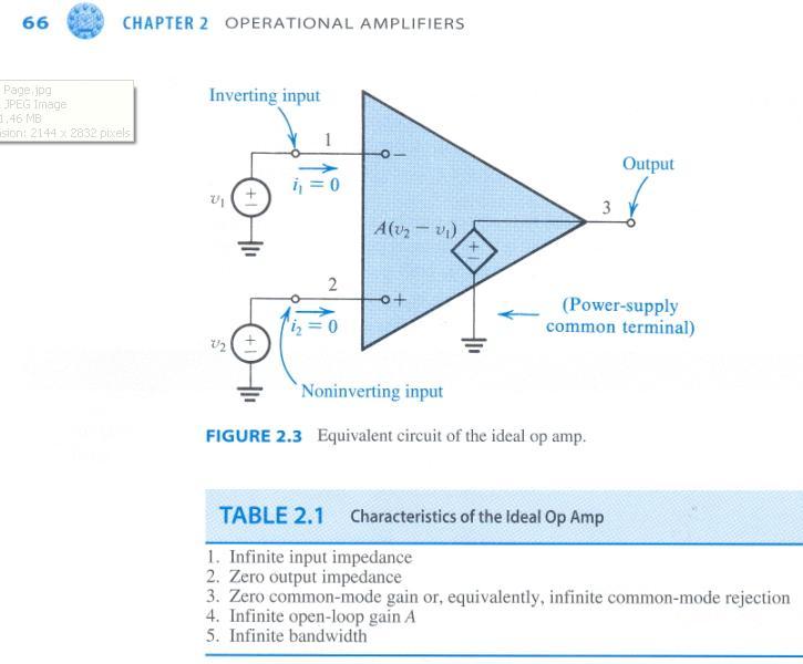
C H A P T E R 02. Operational Amplifiers
 C H A P T E R 02 Operational Amplifiers The Op-amp Figure 2.1 Circuit symbol for the op amp. Figure 2.2 The op amp shown connected to dc power supplies. The Ideal Op-amp 1. Infinite input impedance 2.
Lecture 4: Voltage References
 EE6378 Power Management Circuits Lecture 4: oltage References Instructor: t Prof. Hoi Lee Mixed-Signal & Power IC Laboratory Department of Electrical Engineering The University of Texas at Dallas Introduction
Operational Amplifiers (Op Amps)
") Operational Amplifiers (Op Amps) Introduction * An operational amplifier is modeled as a voltage controlled voltage source. * An operational amplifier has a very high input impedance and a very high gain.
Operational Amplifiers (Op Amps) Introduction * An operational amplifier is modeled as a voltage controlled voltage source. * An operational amplifier has a very high input impedance and a very high gain.
A Multiobjective Optimization based Fast and Robust Design Methodology for Low Power and Low Phase Noise Current Starved VCO Gaurav Sharma 1
 IJSRD - International Journal for Scientific Research & Development Vol. 2, Issue 01, 2014 ISSN (online): 2321-0613 A Multiobjective Optimization based Fast and Robust Design Methodology for Low Power
Novel CCII-based Field Programmable Analog Array and its Application to a Sixth-Order Butterworth LPF
 440 S. A. MAHMOUD, E. A. SOLIMAN, NOVEL CCII-ASED FIELD PROGRAMALE ANALOG ARRA. Novel CCII-based Field Programmable Analog Array and its Application to a Sixth-Order utterworth LPF Soliman MAHMOUD 1,2,
PURPOSE: NOTE: Be sure to record ALL results in your laboratory notebook.
 EE4902 Lab 9 CMOS OP-AMP PURPOSE: The purpose of this lab is to measure the closed-loop performance of an op-amp designed from individual MOSFETs. This op-amp, shown in Fig. 9-1, combines all of the major
Design of Pipeline Analog to Digital Converter
 Design of Pipeline Analog to Digital Converter Vivek Tripathi, Chandrajit Debnath, Rakesh Malik STMicroelectronics The pipeline analog-to-digital converter (ADC) architecture is the most popular topology
Design of Miller Compensated Two-Stage Operational Amplifier for Data Converter Applications
 Design of Miller Compensated Two-Stage Operational Amplifier for Data Converter Applications Prema Kumar. G Shravan Kudikala Casest, School Of Physics Casest, School Of Physics University Of Hyderabad
Input Stage Concerns. APPLICATION NOTE 656 Design Trade-Offs for Single-Supply Op Amps
 Maxim/Dallas > App Notes > AMPLIFIER AND COMPARATOR CIRCUITS Keywords: single-supply, op amps, amplifiers, design, trade-offs, operational amplifiers Apr 03, 2000 APPLICATION NOTE 656 Design Trade-Offs
Final Exam Spring 2012
 1 EE 435 Final Exam Spring 2012 Name Instructions: This is an open-book, open-notes, open computer exam but no collaboration either personal or electronic with anyone except the course instructor is permitted.
NOWADAYS, multistage amplifiers are growing in demand
 1690 IEEE TRANSACTIONS ON CIRCUITS AND SYSTEMS I: REGULAR PAPERS, VOL. 51, NO. 9, SEPTEMBER 2004 Advances in Active-Feedback Frequency Compensation With Power Optimization and Transient Improvement Hoi
4.2.2 Metal Oxide Semiconductor Field Effect Transistor (MOSFET)
") 4.2.2 Metal Oxide Semiconductor Field Effect Transistor (MOSFET) The Metal Oxide Semitonductor Field Effect Transistor (MOSFET) has two modes of operation, the depletion mode, and the enhancement mode.
4.2.2 Metal Oxide Semiconductor Field Effect Transistor (MOSFET) The Metal Oxide Semitonductor Field Effect Transistor (MOSFET) has two modes of operation, the depletion mode, and the enhancement mode.
Lesson number one. Operational Amplifier Basics
 What About Lesson number one Operational Amplifier Basics As well as resistors and capacitors, Operational Amplifiers, or Op-amps as they are more commonly called, are one of the basic building blocks
I1 19u 5V R11 1MEG IDC Q7 Q2N3904 Q2N3904. Figure 3.1 A scaled down 741 op amp used in this lab
 Lab 3: 74 Op amp Purpose: The purpose of this laboratory is to become familiar with a two stage operational amplifier (op amp). Students will analyze the circuit manually and compare the results with SPICE.
Lecture 030 ECE4430 Review III (1/9/04) Page 030-1
 Page 030-1") Lecture 030 ECE4430 Review III (1/9/04) Page 0301 LECTURE 030 ECE 4430 REVIEW III (READING: GHLM Chaps. 3 and 4) Objective The objective of this presentation is: 1.) Identify the prerequisite material
Lecture 030 ECE4430 Review III (1/9/04) Page 0301 LECTURE 030 ECE 4430 REVIEW III (READING: GHLM Chaps. 3 and 4) Objective The objective of this presentation is: 1.) Identify the prerequisite material
Operational Amplifier as A Black Box
 Chapter 8 Operational Amplifier as A Black Box 8. General Considerations 8.2 Op-Amp-Based Circuits 8.3 Nonlinear Functions 8.4 Op-Amp Nonidealities 8.5 Design Examples Chapter Outline CH8 Operational Amplifier
Lecture 240 Cascode Op Amps (3/28/10) Page 240-1
 Page 240-1") Lecture 240 Cascode Op Amps (3/28/10) Page 2401 LECTURE 240 CASCODE OP AMPS LECTURE ORGANIZATION Outline Lecture Organization Single Stage Cascode Op Amps Two Stage Cascode Op Amps Summary CMOS Analog
Lecture 240 Cascode Op Amps (3/28/10) Page 2401 LECTURE 240 CASCODE OP AMPS LECTURE ORGANIZATION Outline Lecture Organization Single Stage Cascode Op Amps Two Stage Cascode Op Amps Summary CMOS Analog
Applied Electronics II
 Applied Electronics II Chapter 3: Operational Amplifier Part 1- Op Amp Basics School of Electrical and Computer Engineering Addis Ababa Institute of Technology Addis Ababa University Daniel D./Getachew
International Journal of Emerging Technologies in Computational and Applied Sciences (IJETCAS)
") International Association of Scientific Innovation and Research (IASIR) (An Association Unifying the Sciences, Engineering, and Applied Research) International Journal of Emerging Technologies in Computational
International Association of Scientific Innovation and Research (IASIR) (An Association Unifying the Sciences, Engineering, and Applied Research) International Journal of Emerging Technologies in Computational
Operational Amplifiers Part IV of VI Working Your Amplifier Inside the Single-Supply Voltage Box
 Operational Amplifiers Part IV of VI Working Your Amplifier Inside the Single-Supply Voltage Box by Bonnie C. Baker Microchip Technology, Inc. bonnie.baker@microchip.com It may seem easy enough to transfer
Friday, 1/27/17 Constraints on A(jω)
") Friday, 1/27/17 Constraints on A(jω) The simplest electronic oscillators are op amp based, and A(jω) is typically a simple op amp fixed gain amplifier, such as the negative gain and positive gain amplifiers
Friday, 1/27/17 Constraints on A(jω) The simplest electronic oscillators are op amp based, and A(jω) is typically a simple op amp fixed gain amplifier, such as the negative gain and positive gain amplifiers
Chapter 12 Opertational Amplifier Circuits
 1 Chapter 12 Opertational Amplifier Circuits Learning Objectives 1) The design and analysis of the two basic CMOS op-amp architectures: the two-stage circuit and the single-stage, folded cascode circuit.
Ultra-Low-Voltage Floating-Gate Transconductance Amplifiers
 IEEE TRANSACTIONS ON CIRCUITS AND SYSTEMS II: ANALOG AND DIGITAL SIGNAL PROCESSING, VOL. 48, NO. 1, JANUARY 2001 37 Ultra-Low-Voltage Floating-Gate Transconductance Amplifiers Yngvar Berg, Tor S. Lande,
A PSEUDO-CLASS-AB TELESCOPIC-CASCODE OPERATIONAL AMPLIFIER
 A PSEUDO-CLASS-AB TELESCOPIC-CASCODE OPERATIONAL AMPLIFIER M. Taherzadeh-Sani, R. Lotfi, and O. Shoaei ABSTRACT A novel class-ab architecture for single-stage operational amplifiers is presented. The structure
ECE 442 Solid State Devices & Circuits. 15. Differential Amplifiers
 ECE 442 Solid State Devices & Circuits 15. Differential Amplifiers Jose E. Schutt-Aine Electrical & Computer Engineering University of Illinois jschutt@emlab.uiuc.edu ECE 442 Jose Schutt Aine 1 Background
ECEN 474/704 Lab 8: Two-Stage Miller Operational Amplifier
 ECEN 474/704 Lab 8: Two-Stage Miller Operational Amplifier Objective Design, simulate and test a two-stage operational amplifier Introduction Operational amplifiers (opamp) are essential components of
Low voltage, low power, bulk-driven amplifier
 University of Arkansas, Fayetteville ScholarWorks@UARK Electrical Engineering Undergraduate Honors Theses Electrical Engineering 5-2009 Low voltage, low power, bulk-driven amplifier Shama Huda University
Design and Implementation of Current-Mode Multiplier/Divider Circuits in Analog Processing
 Design and Implementation of Current-Mode Multiplier/Divider Circuits in Analog Processing N.Rajini MTech Student A.Akhila Assistant Professor Nihar HoD Abstract This project presents two original implementations
Radivoje Đurić, 2015, Analogna Integrisana Kola 1
 Low power OTA 1 Two-Stage, Miller Op Amp Operating in Weak Inversion Low frequency response: gm1 gm6 Av 0 g g g g A v 0 ds2 ds4 ds6 ds7 I D m, ds D nvt g g I n GB and SR: GB 1 1 n 1 2 4 6 6 7 g 2 2 m1
Analysis and Design of a Simple Operational Amplifier
 by Kenneth A. Kuhn December 26, 2004, rev. Jan. 1, 2009 Introduction The purpose of this article is to introduce the student to the internal circuits of an operational amplifier by studying the analysis
Lecture 300 Low Voltage Op Amps (3/28/10) Page 300-1
 Page 300-1") Lecture 300 Low Voltage Op Amps (3/28/10) Page 300-1 LECTURE 300 LOW VOLTAGE OP AMPS LECTURE ORGANIZATION Outline Introduction Low voltage input stages Low voltage gain stages Low voltage bias circuits
Lecture 300 Low Voltage Op Amps (3/28/10) Page 300-1 LECTURE 300 LOW VOLTAGE OP AMPS LECTURE ORGANIZATION Outline Introduction Low voltage input stages Low voltage gain stages Low voltage bias circuits
[Kumar, 2(9): September, 2013] ISSN: Impact Factor: 1.852
![[Kumar, 2(9): September, 2013] ISSN: Impact Factor: 1.852](/thumbs/86/94008668.jpg "[Kumar, 2(9): September, 2013] ISSN: Impact Factor: 1.852") IJESRT INTERNATIONAL JOURNAL OF ENGINEERING SCIENCES & RESEARCH TECHNOLOGY Design and Performance analysis of Low power CMOS Op-Amp Anand Kumar Singh *1, Anuradha 2, Dr. Vijay Nath 3 *1,2 Department of
IJESRT INTERNATIONAL JOURNAL OF ENGINEERING SCIENCES & RESEARCH TECHNOLOGY Design and Performance analysis of Low power CMOS Op-Amp Anand Kumar Singh *1, Anuradha 2, Dr. Vijay Nath 3 *1,2 Department of
Design and Analysis of Current-to-Voltage and Voltage - to-current Converters using 0.35µm technology
 Design and Analysis of Current-to-Voltage and Voltage - to-current Converters using 0.35µm technology Kopal Gupta 1, Prof. B. P Singh 2, Rockey Choudhary 3 1 M.Tech (VLSI Design ) at Mody Institute of
ISSN:
 468 Modeling and Design of a CMOS Low Drop-out (LDO) Voltage Regulator PRIYADARSHINI JAINAPUR 1, CHIRAG SHARMA 2 1 Department of E&CE, Nitte Meenakshi Institute of Technology, Yelahanka, Bangalore-560064,
QUESTION BANK for Analog Electronics 4EC111 *
 OpenStax-CNX module: m54983 1 QUESTION BANK for Analog Electronics 4EC111 * Bijay_Kumar Sharma This work is produced by OpenStax-CNX and licensed under the Creative Commons Attribution License 4.0 Abstract
Problem 1. Final Exam Spring 2018 (Reposted 11p.m. on April 30)
") EE 435 Final Exam Spring 2018 (Reposted 11p.m. on April 30) Name Instructions: This is an open-book, open-notes exam. It is due in the office of the course instructor by 12:00 noon on Wednesday May 2.
EE 435 Final Exam Spring 2018 (Reposted 11p.m. on April 30) Name Instructions: This is an open-book, open-notes exam. It is due in the office of the course instructor by 12:00 noon on Wednesday May 2.
A CMOS Low-Voltage, High-Gain Op-Amp
 A CMOS Low-Voltage, High-Gain Op-Amp G N Lu and G Sou LEAM, Université Pierre et Marie Curie Case 203, 4 place Jussieu, 75252 Paris Cedex 05, France Telephone: (33 1) 44 27 75 11 Fax: (33 1) 44 27 48 37
Design of Low Voltage Low Power CMOS OP-AMPS with Rail-to-Rail Input/Output Swing.
 Design of ow oltage ow Power CMOS OP-AMPS with Rail-to-Rail Input/Output Swing. Mr.S..Gopalaiah Bangalore-56. svg@ece.iisc.ernet.in Prof. A. P. Shivaprasad Bangalore-56. aps@ece.iisc.ernet.in Mr. Sukanta
Sensors & Transducers Published by IFSA Publishing, S. L.,
 Sensors & Transducers Published by IFSA Publishing, S. L., 208 http://www.sensorsportal.com Fully Differential Operation Amplifier Using Self Cascode MOSFET Structure for High Slew Rate Applications Kalpraj
4. Differential Amplifiers. Electronic Circuits. Prof. Dr. Qiuting Huang Integrated Systems Laboratory
 4. Differential Amplifiers Electronic Circuits Prof. Dr. Qiuting Huang Integrated Systems Laboratory Differential Signaling Basics and Motivation Transmitting information with two complementary signals
Design and Simulation of an Operational Amplifier with High Gain and Bandwidth for Switched Capacitor Filters
 IOSR Journal of Electrical and Electronics Engineering (IOSR-JEEE) e-issn: 2278-1676,p-ISSN: 2320-3331, Volume 11, Issue 1 Ver. II (Jan. Feb. 2016), PP 47-53 www.iosrjournals.org Design and Simulation
A Unity Gain Fully-Differential 10bit and 40MSps Sample-And-Hold Amplifier in 0.18μm CMOS
 A Unity Gain Fully-Differential 0bit and 40MSps Sample-And-Hold Amplifier in 0.8μm CMOS Sanaz Haddadian, and Rahele Hedayati Abstract A 0bit, 40 MSps, sample and hold, implemented in 0.8-μm CMOS technology
Analog CMOS Interface Circuits for UMSI Chip of Environmental Monitoring Microsystem
 Analog CMOS Interface Circuits for UMSI Chip of Environmental Monitoring Microsystem A report Submitted to Canopus Systems Inc. Zuhail Sainudeen and Navid Yazdi Arizona State University July 2001 1. Overview