EE 230 Lecture 17. Nonideal Op Amp Characteristics
|
|
|
- Oswald Hutchinson
- 5 years ago
- Views:
Transcription
1 EE 3 Lecture 17 Nonideal Op Amp Characteristics
2 Quiz 11 The dc gain of this circuit was measured to be 5 and the 3dB bandwidth was measured to be 6KHz. Determine as many of the following as possible from this information if it is known that the op amp can be modeled as a single-pole lowpass amplifier. Ao (dc gain of the Op Amp) P (pole of the Op Amp) (gain-bandwidth product of Op Amp) 1 OUT IN 3
3 And the number is?
4 And the number is?
5 Quiz 11 Solution: The dc gain of this circuit was measured to be 5 and the 3dB bandwidth was measured to be 6KHz. Determine as many of the following as possible from this information if it is known that the op amp can be modeled as a single-pole lowpass amplifier. A o (dc gain of the Op Amp) p (pole of the Op Amp) (gain-bandwidth product of Op Amp) Insufficient information to determine A o or 1 R =K BW= 1+ O R 1 BW OUT 3 IN
6 Quiz 11 Solution: 1 The dc gain of this circuit was measured to be 5 and the 3dB bandwidth was measured to be 6KHz. Determine as many of the following as possible from this information if it is known that the op amp can be modeled as a single-pole lowpass amplifier. A o (dc gain of the Op Amp) p (pole of the Op Amp) (gain-bandwidth product of Op Amp) OUT Insufficient information to determine A o or R =K BW= 1+ BW O R 1 =5 6KHz = 3MHz =(18.8M Rad / Sec) IN 3
7 Review from Last Time Instrumentation Amplifier Differential Amplifiers Can reduce effects of dc offset if gain must be very large Must pick C to that frequencies of interest are in passband
8 Review from Last Time Impedance Converters V1( G 1+G ) = VXG I= 1 ( V-V 1 X) G3 ZZ 1 3 Z IN= - Z Observe this input impedance is negative!
9 Review from Last Time Impedance Converters I 1 Z 5 IN V 1 Z 3 Z 4 One Port Z 1 Z Z = IN ZZZ ZZ Z = R C s If Z 1 =Z 3 =Z 4 = Z 5 =R and Z =1/sC IN ( ) If Z =R, Z 3 =R 3, Z 4 =R 4, Z 5 =R 5 and Z 1 =1/sC RR 3 5 Z IN= scr R 4 This is an inductor of value L=R C This is a capacitor of value RR 4 C EQ= C (can scale capacitance up or down) RR 3 5 If Z =Z 4 = Z 5 =R and Z 1 =Z 3 =1/sC IN ( ) 3 Z = R C s 3 This is a super capacitor of value This circuit is often called a Gyrator RC
10 Review from Last Time Nonideal Properties of Operational Amplifiers In even the most basic applications, the laboratory performance of the circuit often differs dramatically from what is predicted for some op amps. With proper knowledge of the characteristics of the op amp, designers can usually design circuits that behave almost like what is expected with ideal op amps Essential to know nonideal properties of the op amp and how to manage them to be an effective design engineer
11 Review from Last Time Some of the more common nonideal effects in Op Amp circuits V IN (t) V OUT (t) VM t t V OUT (t) VDD V OUT (t) t t VSS VDD VDD t t VSS VSS VDD VDD t t VSS VSS VDD t VDD t Will try to identify the source cause of all of these problems and how they can be resolved VSS VSS
 Widlar began his IC career at Fairchild")


12 Review from Last Time Inventor of two-stage Op Amp Robert Widlar (considered by many as the most brilliant integrated circuit designer ever) Widlar began his IC career at Fairchild semiconductor in Sept 63 at age of approx 6 where he designed several pioneering op amps. By 1966, the commercial success of his designs became apparent, and Widlar asked for a raise. He was turned down, and jumped ship to the fledgling National Semiconductor. At National he continued to turn out amazing designs, and was able to retire just before his 3th birthday in 197.
13 Review from Last Time Inventor of the internally-compensated Op Amp Dave Fullagar (from posted www site) Joined Fairchild in Jan 1966 and asked to design an op amp His design was the first internally-compensate op amp, the 741 Fullagar was 6 years old when this was designed (introduced) in 1968 Largest selling integrated circuit ever Still in high-volume production even though over 4 years old Fullagar later started the linear design activities at Intersil Cofounder (catalyst) of Maxim
14 Review from Last Time Nonideal Op Amp Characteristics Absolute Maximum Ratings Electrical Characteristics AC DC These are in the data sheets of the op amps along with connection information, occasionally application information, connection information, and sometimes even information about the design Application notes, available from almost all manufacturers, often give more general information, definitions, more extensive application information, and other useful details.
15 Review from Last Time Widely Varying Performance Characteristics (selected comparison) Model Type Supply Min (V) Supply Max (V) Output Current (ma) Supply Current/ Channel (ma) (MHz) Power (mw) Min Price $ Max Price $ LMP34 (quad) LM741 Micropower General Purpose LM3886 Power , LMP 31 LMH 664 Low Voltage High Speed Minimum Maximum
16 Review from Last Time Nonideal Op Amp Characteristics Critical Parameters Usually Less Critical Parameters Gain-Bandwidth Product () Offset Voltage DC voltage gain, A 3dB Bandwidth, BW =A BW Input Voltage Range Output Voltage Range Output Saturation Current Slew Rate Common Mode Rejection Ratio (CMRR) Power Supply Rejection Ratio (PSRR) R IN and R OUT Bias Currents Full Power Bandwidth Compensation
17 Review from Last Time Gain, Bandwidth and 1 OUT V OUT A( s ) = V-V 1 BW = -p ( ) A -p A( s ) = s-p Since Alternatively ( ) =A -p A( s ) = s-p Almost all op amps are designed to have a first-order response down to unity gain is one of the most important parameters in many op amp applications!
18 Review from Last Time Gain, Bandwidth and Summary of Effects of on Basic Inverting and Noninverting Amplifiers V V 1 A 1 s = s+bw ( ) =A BWA V OUT A R K=1+ R 1 A( s ) = s Adequate model for most applications R K= R 1 BW = K db/ decade 1 BW = 1+K A FB K ( s)= K 1+s db A FB (s) BW A BW A FB ( s) K = ( 1+K ) 1+s
19 Example: Compare the closed-loop BW for an inverting and noninverting amplifier where the magnitude of the closed loop gain is 1. Assume the op amp is MHz. BW = K BW = 1+K BW MHz = = MHz 1 BW MHz = = 1MHz 1+1 Note the difference in BW is significant when the gain is small!
20 Measurement of Most direct: measure A o measure ω b =A o ω b A o is difficult to measure (and exact value usually not of concern) ω b is difficult to measure (and exact value seldom of concern) Direct method of determining is not practical If a circuit is adversely affected be a parameter, then this circuit is often useful for measuring that parameter provided relationship between performance and parameter is determined/known.
21 Strategy for Measuring 1. Build FB noninverting amplifier with gain K o. Measure BW 3. =(K )(BW) Keep gain (K ) quite large (maybe 1) and amplitude small enough so there is no SR distortion. With large K, frequency where gain drops 3dB will be small enough that it can be accurately measured.
22 Example: If an op amp has a of 1MHz and a dc gain of a closed loop amplifier of 1, what is the BW of the closed loop amplifier? Solution: BW 1MHz = = = 1kHz K 1 o Example: Determine the maximun dc gain of a noninverting FB amplifier if designed with an OA with =1MHz, if the closed loop BW must be greater than khz. 1MHz Solution: KBW = Ko = = = 5 BW khz
23 Example: If the input to the amplifier is.1sin(π1t), determine the actual and desired output if the op amp is the LMP31 biased with +/-.5V supplies. R R The desired output is 1+ V =1V = sin ( π 1t ) BW = = K 1 1 IN Need to determine if BW is limiting performance of circuit IN
24
25
26 Example: If the input to the amplifier is.1sin(π1t), determine the actual and desired output if the op amp is the LMP31 biased with +/-.5V supplies. VOUTDesired = sin(π 1 t) ωsig = π 1 13KHz BW = = = 1.3KHz 1 1 Thus input frequency is somewhat higher than band edge FB K K ( ) A s = 1+ s A db/ decade FB ( ) A s = s π 1 db p BW ω sig ω
27 Example: If the input to the amplifier is.1sin(π1t), determine the actual and desired output if the op amp is the LMP31 biased with +/-.5V supplies. VOUTDesired = sin(π 1 t) ωsig = π 1 FB ( ) A s = FB ( ω) A j = ( ω) s π j 1 π 13 1 AFB j = 1+j7.7 FB 1 ( ω ) = 1.9 A j = ( π ) V OUT V OUT db A p db/ decade BW ω sig j7.7 AFB j = -tan = 1-1 ( ω) 8.6 o o =.1*1.9sin(π 1t 8.6 ) o =.1sin(π 1t 8.6 ) ω
28 Addressing Bandwidth Limitations If both amplifiers have the same total gain of A V =1, compare the bandwidths of the two amplifiers if the Op Amps all have the same
29 Addressing Bandwidth Limitations R B K= 1+ R A V V V A CASCADE= = V V V OUT OUT 1 IN 1 IN the frequency-dependent noninverting amplifier was derived earlier: FB ( )= A CASCADE A K K = K K 1+s 1+s ( s) CASCADE ( jω) K = K 1+jω the dc gain is given by K ACASCADE ( j) = K 1 K = = 1+j A s K K 1+s to find the 3dB BW, must solve following ( ) ACASCADE jω K =
30 Addressing Bandwidth Limitations A A CASCADE CASCADE ( jω) ( jω) ( ) ACASCADE jω K = but the gain magnitude of the cascade is given by K K = K = K 1+jω 1+jω K K == = K K 1+ω 1+ω where RB K= 1+ Av 1 R = = K A so, BW CASCADE is the solution of K K = 1+ω 1 ω = K 1 BWCASCADE = K
31 Addressing Bandwidth Limitations 1 BW = A CASCADE V BW = A V (derived before) Comparing the bandwidths with the same A V =1, obtain 1 BW CASCADE= =.64 BW = = A major improvement in BW is possible if a large gain is required! Even more improvement if more stages cascaded if gain is large


32 Determination of proper Op Amp orientation??? If ideal op amps both have gain A FB R =1+ R 1 Usually the good circuit Usually the bad circuit Lets see what happens to the bad to determine if that will give insight into what the problem is
33 Determination of proper Op Amp orientation If ideal op amps both have gain A FB R =1+ R 1 Usually the good circuit Usually the bad circuit If configured as above, the circuit on the left will amplify the signal as desired and that on the right will latch up to either V DD or V SS Sounds like it might be a stability problem associated with a pole on the positive real axis in the RHP
34 Determination of proper Op Amp orientation If ideal op amps both have gain R 1 A FB=1+ = R β 1 Usually the good circuit Usually the bad circuit Check stability with model of Op Amp A( s ) = V1( G 1+G ) = VOUTG s-p V OUT= ( VIN -V1 ) V OUT= - ( VIN -V1 ) s-p s-p V1( G 1+G ) = VOUTG AFB ( s ) = R1 s-p+ R+R 1 - AFB ( s ) = R1 s-p- R+R 1 A FB s = s-p+β ( ) p FB= p-β A FB - s = s-p- β ( ) p FB= p+β
35 Determination of proper Op Amp orientation If ideal op amps both have gain R 1 A FB=1+ = R β 1 Usually the good circuit Usually the bad circuit Check stability with model of Op Amp p FB= p-β p FB= p+β Recall: A system is stable iff all poles of the system lie in the open LHP
36 Determination of proper Op Amp orientation If ideal op amps both have gain R 1 A FB=1+ = R β A( s ) = Usually the good circuit s-p Usually the bad circuit Check stability with model of Op Amp p FB= p-β p FB= p+β 1 Since p is negative, p FB << Pole far in LHP on negative real axis Although p negative, p<<β Pole far in RHP on positive real axis!! Thus, circuit on left is stable but one on right is unstable and thus not useful as an amplifier Would have observed same results with simpler model A( s ) = s
37 Determination of proper Op Amp orientation The good circuit A( s ) = s The bad circuit If we put in the model for A(s) we will find the circuit on the left has all poles in the LHP and the one on the right has a pole far in the RHP on the positive real axis
38 Determination of proper Op Amp orientation Put in frequency dependent model for op amp A( s ) = s in the OVERALL CIRCUIT and determine which orientation of the op amp has all poles in LHP In almost all op amp circuits of interest, there will be a unique op amp orientation that will provide a stable circuit This can be somewhat tedious if there are several op amps because they must all be oriented correctly Experience is useful at providing guidance on how to orient the op amps An unstable circuit can be embedded in a larger circuit that is stable and a stable circuit can be embedded in a larger circuit and make it unstable so can not consider only the stability of a subcircuit but rather must consider the overall circuit One of the major reasons the concept of stability was discussed in this course was to have a method of correctly orienting the op amps in op amp circuits
39 Stability Problems V IN(t) V OUT (t) VM t t V OUT (t) VDD V OUT(t) t t VSS VDD VDD t t VSS VSS VDD VDD t t VSS VSS VDD VDD t t Stability Problem VSS VSS
40 End of Lecture 17
EE 435 Lecture 15. Two-Stage Op Amp Design
 EE 435 Lecture 15 Two-Stage Op Amp Design Review from Last Time Cascaded Amplifier Issues A A 0 p s p Single-stage amplifiers -- widely used in industry, little or no concern about compensation Two amplifier
EE 230 Lecture 19. Nonideal Op Amp Characteristics. Offset Voltage Common-mode input range Compensation
 EE 230 Lecture 19 Nonideal Op Amp Characteristics Offset Voltage Common-mode input range Compensation Quiz 13 The operational amplifier has a GB of 20MHz. Determine the 3dB bandwidth of the closed-loop
Experiment 1: Amplifier Characterization Spring 2019
 Experiment 1: Amplifier Characterization Spring 2019 Objective: The objective of this experiment is to develop methods for characterizing key properties of operational amplifiers Note: We will be using
Chapter 2. Operational Amplifiers
 Chapter 2. Operational Amplifiers Tong In Oh 1 2.5 Integrators and Differentiators Utilized resistors in the op-amp feedback and feed-in path Ideally independent of frequency Use of capacitors together
LM148/LM248/LM348 Quad 741 Op Amps
 Quad 741 Op Amps General Description The LM148 series is a true quad 741. It consists of four independent, high gain, internally compensated, low power operational amplifiers which have been designed to
Lecture Notes Unit-III
 Lecture Notes Unit-III FAQs Q1: An operational amplifier has a differential gain of 103 and CMRR of 100, input voltages are 120µV and 80µV, determine output voltage. 2 MARKS
Friday, 1/27/17 Constraints on A(jω)
") Friday, 1/27/17 Constraints on A(jω) The simplest electronic oscillators are op amp based, and A(jω) is typically a simple op amp fixed gain amplifier, such as the negative gain and positive gain amplifiers
Friday, 1/27/17 Constraints on A(jω) The simplest electronic oscillators are op amp based, and A(jω) is typically a simple op amp fixed gain amplifier, such as the negative gain and positive gain amplifiers
CMOS Operational-Amplifier
 CMOS Operational-Amplifier 1 What will we learn in this course How to design a good OP Amp. Basic building blocks Biasing and Loading Swings and Bandwidth CH2(8) Operational Amplifier as A Black Box Copyright
James Lunsford HW2 2/7/2017 ECEN 607
 James Lunsford HW2 2/7/2017 ECEN 607 Problem 1 Part A Figure 1: Negative Impedance Converter To find the input impedance of the above NIC, we use the following equations: V + Z N V O Z N = I in, V O kr
Operational Amplifier as A Black Box
 Chapter 8 Operational Amplifier as A Black Box 8. General Considerations 8.2 Op-Amp-Based Circuits 8.3 Nonlinear Functions 8.4 Op-Amp Nonidealities 8.5 Design Examples Chapter Outline CH8 Operational Amplifier
Chapter 12 Opertational Amplifier Circuits
 1 Chapter 12 Opertational Amplifier Circuits Learning Objectives 1) The design and analysis of the two basic CMOS op-amp architectures: the two-stage circuit and the single-stage, folded cascode circuit.
PART. Maxim Integrated Products 1
 - + 9-; Rev ; / Low-Cost, High-Slew-Rate, Rail-to-Rail I/O Op Amps in SC7 General Description The MAX9/MAX9/MAX9 single/dual/quad, low-cost CMOS op amps feature Rail-to-Rail input and output capability
LM348. Quad Operational Amplifier. Features. Description. Internal Block Diagram.
 Quad Operational Amplifier www.fairchildsemi.com Features LM741 OP Amp operating characteristics Low supply current drain Class AB output stage-no crossover distortion Pin compatible with the LM324 Low
Homework Assignment 03
 Homework Assignment 03 Question 1 (Short Takes), 2 points each unless otherwise noted. 1. Two 0.68 μf capacitors are connected in series across a 10 khz sine wave signal source. The total capacitive reactance
Applied Electronics II
 Applied Electronics II Chapter 3: Operational Amplifier Part 1- Op Amp Basics School of Electrical and Computer Engineering Addis Ababa Institute of Technology Addis Ababa University Daniel D./Getachew
Thursday, 1/23/19 Automatic Gain Control As previously shown, 1 0 is a nonlinear system that produces a limit cycle with a distorted sinusoid for
 Thursday, 1/23/19 Automatic Gain Control As previously shown, 1 0 is a nonlinear system that produces a limit cycle with a distorted sinusoid for x(t), which is not a very good sinusoidal oscillator. A
CMOS Operational-Amplifier
 CMOS Operational-Amplifier 1 What will we learn in this course How to design a good OP Amp. Basic building blocks Biasing and Loading Swings and Bandwidth CH2(8) Operational Amplifier as A Black Box Copyright
You will be asked to make the following statement and provide your signature on the top of your solutions.
 1 EE 435 Name Exam 1 Spring 2018 Instructions: The points allocated to each problem are as indicated. Note that the first and last problem are weighted more heavily than the rest of the problems. On those
 Distributed by: www.jameco.com 1-800-831-4242 The content and copyrights of the attached material are the property of its owner. LM148/LM248/LM348 Quad 741 Op Amps General Description The LM148 series
LF411 Low Offset, Low Drift JFET Input Operational Amplifier
 Low Offset, Low Drift JFET Input Operational Amplifier General Description These devices are low cost, high speed, JFET input operational amplifiers with very low input offset voltage and guaranteed input
HT9274 Quad Micropower Op Amp
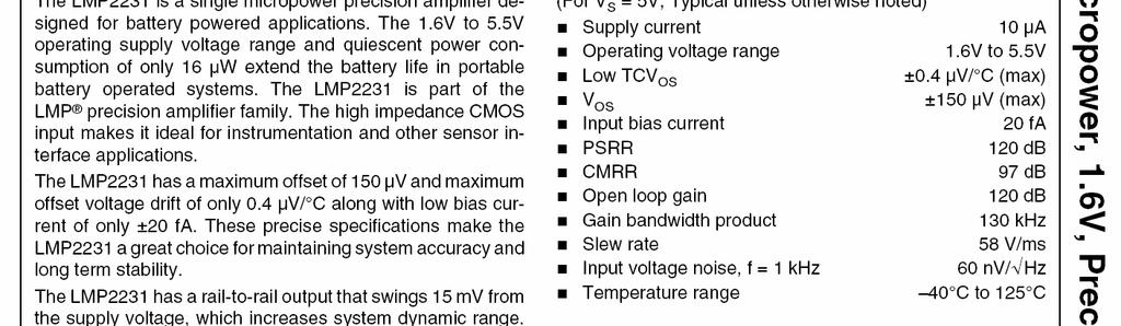
 Quad Micropower Op Amp Features Quad micro power op amp Wide range of supply voltage: 1.6V~5.5V High input impedance Single supply operation Low current consumption: < 5A per amp Rail to rail output Provides
Dual operational amplifier
 DESCRIPTION The 77 is a pair of high-performance monolithic operational amplifiers constructed on a single silicon chip. High common-mode voltage range and absence of latch-up make the 77 ideal for use
Solid State Devices & Circuits. 18. Advanced Techniques
 ECE 442 Solid State Devices & Circuits 18. Advanced Techniques Jose E. Schutt-Aine Electrical l&c Computer Engineering i University of Illinois jschutt@emlab.uiuc.edu 1 Darlington Configuration - Popular
Electric Circuit Theory
 Electric Circuit Theory Nam Ki Min nkmin@korea.ac.kr 010-9419-2320 Chapter 15 Active Filter Circuits Nam Ki Min nkmin@korea.ac.kr 010-9419-2320 Contents and Objectives 3 Chapter Contents 15.1 First-Order
IFB270 Advanced Electronic Circuits
 IFB270 Advanced Electronic Circuits Chapter 12: The operational amplifier Prof. Manar Mohaisen Department of EEC Engineering Review of the Precedent Lecture Introduce the four layer diode Introduce the
nanopower Op Amp in a Tiny 6-Bump WLP
 EVALUATION KIT AVAILABLE MAX4464 General Description The MAX4464 is an ultra-small (6-bump WLP) op amp that draws only 75nA of supply current. It operates from a single +.8V to +5.5V supply and features
Homework Assignment EE 435 Homework 4 Spring 2014 Due Wednesday Feb 26
 Homework Assignment EE 435 Homework 4 Spring 2014 Due Wednesday Feb 26 In the following problems, if reference to a semiconductor process is needed, assume processes with the following characteristics:
ECE 363 FINAL (F16) 6 problems for 100 pts Problem #1: Fuel Pump Controller (18 pts)
 6 problems for 100 pts Problem #1: Fuel Pump Controller (18 pts)") ECE 363 FINAL (F16) NAME: 6 problems for 100 pts Problem #1: Fuel Pump Controller (18 pts) You are asked to design a high-side switch for a remotely operated fuel pump. You decide to use the IRF9520 power
ECE 363 FINAL (F16) NAME: 6 problems for 100 pts Problem #1: Fuel Pump Controller (18 pts) You are asked to design a high-side switch for a remotely operated fuel pump. You decide to use the IRF9520 power
Chapter 10: Operational Amplifiers
 Chapter 10: Operational Amplifiers Differential Amplifier Differential amplifier has two identical transistors with two inputs and two outputs. 2 Differential Amplifier Differential amplifier has two identical
TL082 Wide Bandwidth Dual JFET Input Operational Amplifier
 TL082 Wide Bandwidth Dual JFET Input Operational Amplifier General Description These devices are low cost, high speed, dual JFET input operational amplifiers with an internally trimmed input offset voltage
Frequency Responses and Active Filter Circuits
 Frequency Responses and Active Filter Circuits Compensation capacitors and parasitic capacitors will influence the frequency response Capacitors are also purposely added to create certain functions; e.g.
LF444 Quad Low Power JFET Input Operational Amplifier
 LF444 Quad Low Power JFET Input Operational Amplifier General Description The LF444 quad low power operational amplifier provides many of the same AC characteristics as the industry standard LM148 while
Homework Assignment 13
 Question 1 Short Takes 2 points each. Homework Assignment 13 1. Classify the type of feedback uses in the circuit below (i.e., shunt-shunt, series-shunt, ) Answer: Series-shunt. 2. True or false: an engineer
Operational Amplifier BME 360 Lecture Notes Ying Sun
 Operational Amplifier BME 360 Lecture Notes Ying Sun Characteristics of Op-Amp An operational amplifier (op-amp) is an analog integrated circuit that consists of several stages of transistor amplification
Analog Electronics. Lecture Pearson Education. Upper Saddle River, NJ, All rights reserved.
 Analog Electronics V Lecture 5 V Operational Amplifers Op-amp is an electronic device that amplify the difference of voltage at its two inputs. V V 8 1 DIP 8 1 DIP 20 SMT 1 8 1 SMT Operational Amplifers
LF353 Wide Bandwidth Dual JFET Input Operational Amplifier
 LF353 Wide Bandwidth Dual JFET Input Operational Amplifier General Description These devices are low cost, high speed, dual JFET input operational amplifiers with an internally trimmed input offset voltage
Operational Amplifiers. Boylestad Chapter 10
 Operational Amplifiers Boylestad Chapter 10 DC-Offset Parameters Even when the input voltage is zero, an op-amp can have an output offset. The following can cause this offset: Input offset voltage Input
Experiments #7. Operational Amplifier part 1
 Experiments #7 Operational Amplifier part 1 1) Objectives: The objective of this lab is to study operational amplifier (op amp) and its applications. We will be simulating and building some basic op-amp
Precision, High-Bandwidth Op Amp
 EVALUATION KIT AVAILABLE MAX9622 General Description The MAX9622 op amp features rail-to-rail output and MHz GBW at just 1mA supply current. At power-up, this device autocalibrates its input offset voltage
LM321 Low Power Single Op Amp
 Low Power Single Op Amp General Description The LM321 brings performance and economy to low power systems. With a high unity gain frequency and a guaranteed 0.4V/µs slew rate, the quiescent current is
LF412 Low Offset, Low Drift Dual JFET Input Operational Amplifier
 LF412 Low Offset, Low Drift Dual JFET Input Operational Amplifier General Description These devices are low cost, high speed, JFET input operational amplifiers with very low input offset voltage and guaranteed
Lecture 110 Intro. and Characterization of the Op Amp (1/28/02) Page 110-1
 Page 110-1") Lecture 110 Intro. and Characterization of the Op Amp (1/28/02) Page 1101 LECTURE 110 INTRODUCTION AND CHARACTERIZATION OF THE OP AMP (READING: GHLM 404424, AH 243249) Objective The objective of this presentation
Lecture 110 Intro. and Characterization of the Op Amp (1/28/02) Page 1101 LECTURE 110 INTRODUCTION AND CHARACTERIZATION OF THE OP AMP (READING: GHLM 404424, AH 243249) Objective The objective of this presentation
LP2902/LP324 Micropower Quad Operational Amplifier
 LP2902/LP324 Micropower Quad Operational Amplifier General Description The LP324 series consists of four independent, high gain internally compensated micropower operational amplifiers. These amplifiers
Microelectronic Circuits - Fifth Edition Sedra/Smith Copyright 2004 by Oxford University Press, Inc.
 Feedback 1 Figure 8.1 General structure of the feedback amplifier. This is a signal-flow diagram, and the quantities x represent either voltage or current signals. 2 Figure E8.1 3 Figure 8.2 Illustrating
You will be asked to make the following statement and provide your signature on the top of your solutions.
 1 EE 435 Name Exam 1 Spring 216 Instructions: The points allocated to each problem are as indicated. Note that the first and last problem are weighted more heavily than the rest of the problems. On those
Features. Ordering Information. Part Identification
 MIC9 MHz Low-Power SC-7 Op Amp General Description The MIC9 is a high-speed operational amplifier with a gain-bandwidth product of MHz. The part is unity gain stable. It has a very low.ma supply current,
Input Stage Concerns. APPLICATION NOTE 656 Design Trade-Offs for Single-Supply Op Amps
 Maxim/Dallas > App Notes > AMPLIFIER AND COMPARATOR CIRCUITS Keywords: single-supply, op amps, amplifiers, design, trade-offs, operational amplifiers Apr 03, 2000 APPLICATION NOTE 656 Design Trade-Offs
Single/Dual/Quad, +1.8V/750nA, SC70, Rail-to-Rail Op Amps
 9-; Rev 4; 7/ Single/Dual/Quad, +.8V/75nA, SC7, General Description The MAX4464/MAX447/MAX447/MAX447/MAX4474 family of micropower op amps operate from a single +.8V to +5.5V supply and draw only 75nA of
Op-Amp Simulation Part II
 Op-Amp Simulation Part II EE/CS 5720/6720 This assignment continues the simulation and characterization of a simple operational amplifier. Turn in a copy of this assignment with answers in the appropriate
Designing Information Devices and Systems II Fall 2018 Elad Alon and Miki Lustig Homework 4
 EECS 16B Designing Information Devices and Systems II Fall 2018 Elad Alon and Miki Lustig Homework 4 This homework is solely for your own practice. However, everything on it is in scope for midterm 1,
TL082 Wide Bandwidth Dual JFET Input Operational Amplifier
 TL082 Wide Bandwidth Dual JFET Input Operational Amplifier General Description These devices are low cost, high speed, dual JFET input operational amplifiers with an internally trimmed input offset voltage
Features. Ordering Information. Part Number Standard Marking Pb-Free Marking
 MIC9 MIC9 8MHz Low-Power SC-7 Op Amp General Description The MIC9 is a high-speed operational amplifier with a gain-bandwidth product of 8MHz. The part is unity gain stable. It has a very low µa supply
Type Ordering Code Package TAE 4453 G Q67000-A2152 P-DSO-14-1 (SMD) TAF 4453 G Q67000-A2213 P-DSO-14-1 (SMD)
 TAF 4453 G Q67000-A2213 P-DSO-14-1 (SMD)") Quad PNP-Operational Amplifier TAE 4453 Bipolar IC Features Supply voltage range between 3 and 36 Low current consumption, 1.6 ma typ. Extremely large control range Low output saturation voltage, almost
Quad PNP-Operational Amplifier TAE 4453 Bipolar IC Features Supply voltage range between 3 and 36 Low current consumption, 1.6 ma typ. Extremely large control range Low output saturation voltage, almost
RC4741 General Purpose Operation Amplifier
 General Purpose Operation Amplifier www.fairchildsemi.com Features Unity gain bandwidth 3. MHz High slew rate 1.6 V/mS Low noise voltage 9 nv/öhz Input offset voltage. mv Input bias current 6 na Indefinite
Filters and Tuned Amplifiers
 CHAPTER 6 Filters and Tuned Amplifiers Introduction 55 6. Filter Transmission, Types, and Specification 56 6. The Filter Transfer Function 60 6.7 Second-Order Active Filters Based on the Two-Integrator-Loop
Combination Notch and Bandpass Filter
 Combination Notch and Bandpass Filter Clever filter design for graphic equalizer can perform both notch and bandpass functions Gain or attenuation is controlled by a potentiometer for specific frequency
Lecture #2 Operational Amplifiers
 Spring 2015 Benha University Faculty of Engineering at Shoubra ECE-322 Electronic Circuits (B) Lecture #2 Operational Amplifiers Instructor: Dr. Ahmad El-Banna Agenda Introduction Op-Amps Input Modes and
Operational Amplifiers
 Questions Easy Operational Amplifiers 1. Which of the following statements are true? a. An op-amp has two inputs and three outputs b. An op-amp has one input and two outputs c. An op-amp has two inputs
RC4156/RC4157. High Performance Quad Operational Amplifiers. Features. Description. Block Diagram. Pin Assignments.
 www.fairchildsemi.com RC45/RC457 High Performance Quad Operational Amplifiers Features Unity gain bandwidth for RC45.5 MHz Unity gain bandwidth for RC457 9 MHz High slew rate for RC45. V/mS High slew rate
Linear IC s and applications
 Questions and Solutions PART-A Unit-1 INTRODUCTION TO OP-AMPS 1. Explain data acquisition system Jan13 DATA ACQUISITION SYSYTEM BLOCK DIAGRAM: Input stage Intermediate stage Level shifting stage Output
ELM824xA 3.0μA Very low power CMOS dual operational amplifier
 ELM824xA 3.μA Very low power CMOS dual operational amplifier General description ELM824xA is a very low current consumption-typ.3.μa CMOS dual OP-AMP provided with a wide common mode input voltage range.
OPERATIONAL AMPLIFIER PREPARED BY, PROF. CHIRAG H. RAVAL ASSISTANT PROFESSOR NIRMA UNIVRSITY
 OPERATIONAL AMPLIFIER PREPARED BY, PROF. CHIRAG H. RAVAL ASSISTANT PROFESSOR NIRMA UNIVRSITY INTRODUCTION Op-Amp means Operational Amplifier. Operational stands for mathematical operation like addition,
LF442 Dual Low Power JFET Input Operational Amplifier
 LF442 Dual Low Power JFET Input Operational Amplifier General Description The LF442 dual low power operational amplifiers provide many of the same AC characteristics as the industry standard LM1458 while
Precision, Low-Power and Low-Noise Op Amp with RRIO
 MAX41 General Description The MAX41 is a low-power, zero-drift operational amplifier available in a space-saving, 6-bump, wafer-level package (WLP). Designed for use in portable consumer, medical, and
LF444 Quad Low Power JFET Input Operational Amplifier
 LF444 Quad Low Power JFET Input Operational Amplifier General Description The LF444 quad low power operational amplifier provides many of the same AC characteristics as the industry standard LM148 while
EE 330 Laboratory 8 Discrete Semiconductor Amplifiers
 EE 330 Laboratory 8 Discrete Semiconductor Amplifiers Fall 2017 Contents Objective:... 2 Discussion:... 2 Components Needed:... 2 Part 1 Voltage Controlled Amplifier... 2 Part 2 Common Source Amplifier...
LM6118/LM6218 Fast Settling Dual Operational Amplifiers
 Fast Settling Dual Operational Amplifiers General Description The LM6118/LM6218 are monolithic fast-settling unity-gain-compensated dual operational amplifiers with ±20 ma output drive capability. The
LF451 Wide-Bandwidth JFET-Input Operational Amplifier
 LF451 Wide-Bandwidth JFET-Input Operational Amplifier General Description The LF451 is a low-cost high-speed JFET-input operational amplifier with an internally trimmed input offset voltage (BI- FET IITM
LM833 Dual Audio Operational Amplifier
 LM833 Dual Audio Operational Amplifier General Description The LM833 is a dual general purpose operational amplifier designed with particular emphasis on performance in audio systems. This dual amplifier
A 16Ω Audio Amplifier with 93.8 mw Peak loadpower and 1.43 quiscent power consumption
 A 16Ω Audio Amplifier with 93.8 mw Peak loadpower and 1.43 quiscent power consumption IEEE Transactions on circuits and systems- Vol 59 No:3 March 2012 Abstract A class AB audio amplifier is used to drive
MIC915. Features. General Description. Applications. Ordering Information. Pin Configuration. Pin Description. Dual 135MHz Low-Power Op Amp
 MIC915 Dual 135MHz Low-Power Op Amp General Description The MIC915 is a high-speed, unity-gain stable operational amplifier. It provides a gain-bandwidth product of 135MHz with a very low, 2.4mA supply
LM13600 Dual Operational Transconductance Amplifiers with Linearizing Diodes and Buffers
 LM13600 Dual Operational Transconductance Amplifiers with Linearizing Diodes and Buffers General Description The LM13600 series consists of two current controlled transconductance amplifiers each with
Physics 116A Notes Fall 2004
 Physics 116A Notes Fall 2004 David E. Pellett Draft v.0.9 beta Notes Copyright 2004 David E. Pellett unless stated otherwise. References: Text for course: Fundamentals of Electrical Engineering, second
Operational Amplifiers
 Operational Amplifiers Here we see two matched differential amps cascaded to form a basic OPAMP. The differential pair cancel temperature drifts and common mode noise at the input. First built to perform
EE LINEAR INTEGRATED CIRCUITS & APPLICATIONS
 UNITII CHARACTERISTICS OF OPAMP 1. What is an opamp? List its functions. The opamp is a multi terminal device, which internally is quite complex. It is a direct coupled high gain amplifier consisting of
EE 330 Lecture 20. Operating Points for Amplifier Applications Amplification with Transistor Circuits Small Signal Modelling
 EE 330 Lecture 20 Operating Points for Amplifier Applications Amplification with Transistor Circuits Small Signal Modelling Review from Last Lecture Simplified Multi-Region Model Alternate equivalent model
Lecture 8: More on Operational Amplifiers (Op Amps)
") Lecture 8: More on Operational mplifiers (Op mps) Input Impedance of Op mps and Op mps Using Negative Feedback: Consider a general feedback circuit as shown. ssume that the amplifier has input impedance
Lecture 8: More on Operational mplifiers (Op mps) Input Impedance of Op mps and Op mps Using Negative Feedback: Consider a general feedback circuit as shown. ssume that the amplifier has input impedance
University of Pittsburgh
 University of Pittsburgh Experiment #1 Lab Report Frequency Response of Operational Amplifiers Submission Date: 05/29/2018 Instructors: Dr. Ahmed Dallal Shangqian Gao Submitted By: Nick Haver & Alex Williams
LM837 Low Noise Quad Operational Amplifier
 LM837 Low Noise Quad Operational Amplifier General Description The LM837 is a quad operational amplifier designed for low noise, high speed and wide bandwidth performance. It has a new type of output stage
EE 230 Lecture 23. Nonlinear Op Amp Applications. Waveform Generators
 EE 230 Lecture 23 Nonlinear Op Amp Applications Waveform Generators Quiz 7 An oscillator based upon a comparator with hysteresis is shown. If STAH =2 and SATL =-2, determine the peak value of And the number
Chapter 10 Feedback ECE 3120 Microelectronics II Dr. Suketu Naik
 1 Chapter 10 Feedback Operational Amplifier Circuit Components 2 1. Ch 7: Current Mirrors and Biasing 2. Ch 9: Frequency Response 3. Ch 8: Active-Loaded Differential Pair 4. Ch 10: Feedback 5. Ch 11: Output
Homework Assignment 04
 Question 1 (Short Takes) Homework Assignment 04 1. Consider the single-supply op-amp amplifier shown. What is the purpose of R 3? (1 point) Answer: This compensates for the op-amp s input bias current.
LMC6081 Precision CMOS Single Operational Amplifier
 LMC6081 Precision CMOS Single Operational Amplifier General Description The LMC6081 is a precision low offset voltage operational amplifier, capable of single supply operation. Performance characteristics
QUAD OPERATIONAL AMPLIFIERS FEATURES. SCHEMATIC DIAGRAM (One Section Only)
") S The LM248/LM348 is a true quad LM741. It consists of four independent, high-gain, internally compensated, low-power operational amplifiers which have been designed to provide functional characteristics
S The LM248/LM348 is a true quad LM741. It consists of four independent, high-gain, internally compensated, low-power operational amplifiers which have been designed to provide functional characteristics
HT9291/HT9292/HT9294 TinyPower TM Operation Amplifier
 TinyPower TM Operation Amplifier Features Wide operating voltage: 1.4V to 5.5V Low quiescent current: typical 0.6µA/amplifier Rail-to-Rail output Gain bandwidth: 11kHz typical Unity gain stable Available
High Common-Mode Rejection. Differential Line Receiver SSM2141 REV. B FUNCTIONAL BLOCK DIAGRAM FEATURES. High Common-Mode Rejection
 a FEATURES High Common-Mode Rejection DC: 100 db typ 60 Hz: 100 db typ 20 khz: 70 db typ 40 khz: 62 db typ Low Distortion: 0.001% typ Fast Slew Rate: 9.5 V/ s typ Wide Bandwidth: 3 MHz typ Low Cost Complements
Dual, Ultralow Distortion, Ultralow Noise Op Amp AD8599
 Dual, Ultralow Distortion, Ultralow Noise Op Amp FEATURES Low noise: 1 nv/ Hz at 1 khz Low distortion: 5 db THD @ khz
EC MHz, CMOS, Rail-to-Rail Output Operational Amplifier. General Description. Features. Applications. Pin Configurations(Top View)
") General Description The is wideband, low-noise, low-distortion operational amplifier, that offer rail-to-rail output and single-supply operation down to 2.2V. They draw 5.6mA of quiescent supply current,
General Description The is wideband, low-noise, low-distortion operational amplifier, that offer rail-to-rail output and single-supply operation down to 2.2V. They draw 5.6mA of quiescent supply current,
Features. Applications
 105MHz Low-Power SOT23-5 Op Amp General Description The is a high-speed operational amplifier which is unity gain stable regardless of resistive and capacitive load. It provides a gain-bandwidth product
HT9231/HT9232/HT9234 Operation Amplifier
 Operation Amplifier Features Operating Voltage: 2.0V to 5.5V Supply Current: 220μA/amplifier typical Rail-to-Rail Output Gain Bandwidth: 2.3MHz typical Unity Gain Stable Available in Single, Dual and Quad
UNISONIC TECHNOLOGIES CO., LTD LM321
 UNISONIC TECHNOLOGIES CO., LTD LM321 LOW POWER SINGLE OP AMP DESCRIPTION The UTC LM321 s quiescent current is only 430µA (5V). The UTC LM321 brings performance and economy to low power systems, With a
Design Analysis and Performance Comparison of Low Power High Gain 2nd Stage Differential Amplifier Along with 1st Stage
 Design Analysis and Performance Comparison of Low Power High Gain 2nd Stage Differential Amplifier Along with 1st Stage Sadeque Reza Khan Department of Electronic and Communication Engineering, National
Lecture 2: Non-Ideal Amps and Op-Amps
 Lecture 2: Non-Ideal Amps and Op-Amps Prof. Ali M. Niknejad Department of EECS University of California, Berkeley Practical Op-Amps Linear Imperfections: Finite open-loop gain (A 0 < ) Finite input resistance
PURPOSE: NOTE: Be sure to record ALL results in your laboratory notebook.
 EE4902 Lab 9 CMOS OP-AMP PURPOSE: The purpose of this lab is to measure the closed-loop performance of an op-amp designed from individual MOSFETs. This op-amp, shown in Fig. 9-1, combines all of the major
LF453 Wide-Bandwidth Dual JFET-Input Operational Amplifiers
 LF453 Wide-Bandwidth Dual JFET-Input Operational Amplifiers General Description The LF453 is a low-cost high-speed dual JFET-input operational amplifier with an internally trimmed input offset voltage
Homework Assignment 13
 Question 1 Short Takes 2 points each. Homework Assignment 13 1. Classify the type of feedback uses in the circuit below (i.e., shunt-shunt, series-shunt, ) 2. True or false: an engineer uses series-shunt
Operational Amplifier: Characteristics and Open-Loop Op-Amp
 Lesson: Operational Amplifier: Characteristics and Open- Loop Op- Amp Lesson Developer: Dr. Arun Vir Singh College/Department: Shivaji College, University of Delhi Institute of Lifelong Learning, Delhi
TL082 Wide Bandwidth Dual JFET Input Operational Amplifier
 TL082 Wide Bandwidth Dual JFET Input Operational Amplifier General Description These devices are low cost high speed dual JFET input operational amplifiers with an internally trimmed input offset voltage
Active Filter Design Techniques
 Active Filter Design Techniques 16.1 Introduction What is a filter? A filter is a device that passes electric signals at certain frequencies or frequency ranges while preventing the passage of others.
Design of High-Speed Op-Amps for Signal Processing
 Design of High-Speed Op-Amps for Signal Processing R. Jacob (Jake) Baker, PhD, PE Professor and Chair Boise State University 1910 University Dr. Boise, ID 83725-2075 jbaker@ieee.org Abstract - As CMOS