THE WAFER FAB CLEANS IN SEMICONDUCTOR INDUSTRY FROM A MATERIALS SUPPLIER PERSPECTIVE
|
|
|
- Kimberly Harrington
- 5 years ago
- Views:
Transcription

1 THE WAFER FAB CLEANS IN SEMICONDUCTOR INDUSTRY FROM A MATERIALS SUPPLIER PERSPECTIVE Tianniu Rick Chen, Ph.D. General Manager SP&C Business (Surface Preparation & Cleans)
2 OUTLINE Market drivers and challenges Technology advancements and challenges Questions and answers
3 THERE ARE FORCES ACTING ON MATERIAL SUPPLIERS Regional focus (Asia) Wafer starts/ New applications Industry Consolidation Market Dynamics Wet Cleans Suppliers Technology Dynamics Competing Technologies Safer Products Technology Roadmaps
 sales Growing at a")

4 IC INDUSTRY VALUE CHAIN Wet cleans (excluding pcmp) Sales ~$1.5B in 2018 ~3% of total materials and ~7 of wafer fab materials (excluding substrates and photomasks) sales Growing at a CAGR of 5% Core to SEMI Innovation and Productivity Electronic speciality gases 2% Deposition materials 9% CMP consumable 5% Lithography materials 8% Bulk gases 4% PVD targets 1% Packaging materials 42% Wet cleans 3% Photomasks 7% Substrate (SOI) 1% Substrate (Si) 18% Source: SEMI, Linx consulting

 >70% Of")

")
")
5 WHAT DRIVES WET WAFER FAB CLEANS? Industry Volume Growth - Silicon MSI/Wafer Starts - 4.8% CAGR of MSI ( ) >70% Of All Wafer Starts at 28nm and above Source: IHS MARKIT Technology Changes Due to New Device Architectures - Next Generation Nodes (New Materials) - 3 Dimensional Structures (More materials and More processing steps) Moore s law continues Source: IMEC


6 CUSTOMERS ARE CHANGING Fewer and much larger customers Too many suppliers for shrinking customer base Increased ramp complexity, volume and variability Higher expectations/pressure Access is critical for more limited POR opportunities Implications of winning/losing Customer centric vs. market centric model Giga-sized fab - L18 of Samsung at Pyeongtaek Source: VLSI Research Source: SEMI

7 CUSTOMERS ARE CHANGING Shift to Asia requires footprint changes New customers Supply Operation Innovation infrastructure Source: SEMI The Emergence of Si China Multinational vs. domestic fabs Localization vs. globalization
.")
 spun off As Versum Materials on October 4, 2016 Recent M&As China South Korea Cabot Microelectronics - NexPlanar Entegis - ATMI Fujifilm EM Ultra Pure")
8 COMPETITORS ARE CHANGING Air Products and Chemicals acquired Ashland Specialty Chemical Company's electronic chemicals unit. Acquired Dynaloy LLC, a leading supplier of formulated cleaning solutions from Eastman Chemical Company (NYSE: EMN) Increase Sustainable 80% Growth Air Products founded in Detroit, Michigan, based on Leonard Pool s revolutionary on-site gas supply concept. Air Products EMD (Electronic Materials Division) spun off As Versum Materials on October 4, 2016 Recent M&As China South Korea Cabot Microelectronics - NexPlanar Entegis - ATMI Fujifilm EM Ultra Pure Wonik Nova-Kem NATA - Kempur Air Liquide AirGas + Voltaix SK - OCIM + Tri-Chem Dow Chemical DuPont + Dow Corning Yoke UPChem FFEM - Wako SK Holding LG Siltron Linde + Praxair Infineon - Mentor Avantor - Gelest Global Wafer - SunEdison Leveraged government equity positions to enable significant sized acquisitions Continued acquisition activity from multiple companies. Acquisitions along the line of key product areas: Silicon Gases Lithography materials Advanced deposition materials Korean companies also looking to change business model Gain international market access


9 GREATER NEED FOR INNOVATION SELECTIVE CLEANS New materials challenges Source: Carver, C. et. Al. ECS Journal of Solid State Science and Technology, 4 (6) N5005-N5009, FinFET GAA transistor 3D NAND Vertical geometry challenges Source: AMAT Tight space High A/R
")
 Meeting, October 1 to 5, 2017,")

10 GREATER NEED FOR INNOVATION SELECTIVE CLEANS (CONTINUED) Competing technology of wet cleaning ALE (Atomic Layer Etching) of SiNx Pre- Post- Pre- Post- Source: Hitachi, The 232 nd Electrochemical Society (ECS) Meeting, October 1 to 5, 2017, National Harbor, Maryland. Source: Sherpa, S., et. al. Journal of Vacuum Science & Technology A: Vacuum, Surfaces, and Films 35, 05C310, 2017.
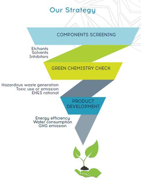
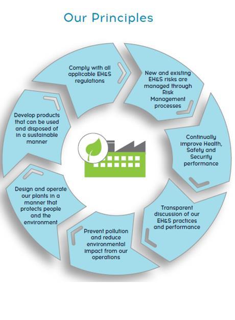
11 OUR COMMITMENT TO SAFER PRODUCTS Our values 11


12 CRITERIA FOR SUCCESS GOING INTO THE 2020S Customer Relationships Innovation Capabilities and Intellectual Property Global Infrastructure and Reliable Supply Diversified Portfolio SEMI Next Generation Specialty Materials Supplier Grace, Elegance and Fortitude
13 THANK YOU Wednesday, April 11th, 2018, 10:40 AM: Development of Wet-Etch Chemistries for Tungsten Word-line Recess by C.K. Ge, Versum Materials
21 st Annual Needham Growth Conference
 21 st Annual Needham Growth Conference Investor Presentation January 15, 2019 Safe Harbor Statement The information contained in and discussed during this presentation may include forward-looking statements
The Development of the Semiconductor CVD and ALD Requirement
 The Development of the Semiconductor CVD and ALD Requirement 1 Linx Consulting 1. We create knowledge and develop unique insights at the intersection of electronic thin film processes and the chemicals
A Perspective on Semiconductor Equipment. R. B. Herring March 4, 2004
 A Perspective on Semiconductor Equipment R. B. Herring March 4, 2004 Outline Semiconductor Industry Overview of circuit fabrication Semiconductor Equipment Industry Some equipment business strategies Product
Innovation to Advance Moore s Law Requires Core Technology Revolution
 Innovation to Advance Moore s Law Requires Core Technology Revolution Klaus Schuegraf, Ph.D. Chief Technology Officer Silicon Systems Group Applied Materials UC Berkeley Seminar March 9 th, 2012 Innovation
Legacy & Leading Edge Both are Winners
 Legacy & Leading Edge Both are Winners Semicon CMP User Group July 16, 2015 Sue Davis 408-833-5905 CMP Team Contributors: Mike Fury, Ph.D. Karey Holland, Ph.D. Jerry Yang, Ph.D. www.techcet.com 1 Outline
Photoresists & Ancillaries. Materials for Semiconductor Manufacturing A TECHCET Critical Materials Report
 2018-19 Photoresists & Ancillaries Materials for Semiconductor Manufacturing A TECHCET Critical Materials Report Prepared by Ed Korczynski Reviewed and Edited by Lita Shon-Roy TECHCET CA LLC PO Box 3814
IMPACT OF 450MM ON CMP
 IMPACT OF 450MM ON CMP MICHAEL CORBETT MANAGING PARTNER LINX CONSULTING, LLC MCORBETT@LINX-CONSULTING.COM PREPARED FOR CMPUG JULY 2011 LINX CONSULTING Outline 1. Overview of Linx Consulting 2. CMP Outlook/Drivers
ACCELERATING THE FUTURE OF SEMICONDUCTORS
 ACCELERATING THE FUTURE OF SEMICONDUCTORS 14 PRODUCTION FACILITIES 7R&D FACILITIES 10+ COUNTRIES VERSUM MATERIALS BY THE NUMBERS* *Fiscal year ending September 30, 2018. 250+ CUSTOMERS CORE INDUSTRIES
HOW TO CONTINUE COST SCALING. Hans Lebon
 HOW TO CONTINUE COST SCALING Hans Lebon OUTLINE Scaling & Scaling Challenges Imec Technology Roadmap Wafer size scaling : 450 mm 2 COST SCALING IMPROVED PERFORMANCE 3 GLOBAL TRAFFIC FORECAST Cloud Traffic
CMOS Digital Integrated Circuits Lec 2 Fabrication of MOSFETs
 CMOS Digital Integrated Circuits Lec 2 Fabrication of MOSFETs 1 CMOS Digital Integrated Circuits 3 rd Edition Categories of Materials Materials can be categorized into three main groups regarding their
Newer process technology (since 1999) includes :
 includes :") Newer process technology (since 1999) includes : copper metalization hi-k dielectrics for gate insulators si on insulator strained silicon lo-k dielectrics for interconnects Immersion lithography for masks
Newer process technology (since 1999) includes : copper metalization hi-k dielectrics for gate insulators si on insulator strained silicon lo-k dielectrics for interconnects Immersion lithography for masks
Fin-Shaped Field Effect Transistor (FinFET) Min Ku Kim 03/07/2018
 Min Ku Kim 03/07/2018") Fin-Shaped Field Effect Transistor (FinFET) Min Ku Kim 03/07/2018 ECE 658 Sp 2018 Semiconductor Materials and Device Characterizations OUTLINE Background FinFET Future Roadmap Keeping up w/ Moore s Law
Fin-Shaped Field Effect Transistor (FinFET) Min Ku Kim 03/07/2018 ECE 658 Sp 2018 Semiconductor Materials and Device Characterizations OUTLINE Background FinFET Future Roadmap Keeping up w/ Moore s Law
Property right statement: Copyright of charts, tables and sentences in this report belongs to
 The Vertical Portal for China Business Intelligence. Semiconductor Equipment Industry Report, 2009 Nov/2009 Property right statement: Copyright of charts, tables and sentences in this report belongs to
David B. Miller Vice President & General Manager September 28, 2005
 Electronic Technologies Business Overview David B. Miller Vice President & General Manager September 28, 2005 Forward Looking Statement During the course of this meeting we may make forward-looking statements.
420 Intro to VLSI Design
 Dept of Electrical and Computer Engineering 420 Intro to VLSI Design Lecture 0: Course Introduction and Overview Valencia M. Joyner Spring 2005 Getting Started Syllabus About the Instructor Labs, Problem
Beyond Moore the challenge for Europe
 Beyond Moore the challenge for Europe Dr. Alfred J. van Roosmalen Vice-President Business Development, NXP Semiconductors Company member of MEDEA+/CATRENE/AENEAS/Point-One FIT-IT 08 Spring Research Wien,
CMP: Where have we been and where are we headed next? Robert L. Rhoades, Ph.D. NCCAVS CMPUG Meeting at Semicon West San Francisco, July 10, 2013
 CMP: Where have we been and where are we headed next? Robert L. Rhoades, Ph.D. NCCAVS CMPUG Meeting at Semicon West San Francisco, July 10, 2013 Outline Where have we been? Semiconductor Industry Birth
ISMI Industry Productivity Driver
 SEMATECH Symposium Japan September 15, 2010 Accelerating Manufacturing Productivity ISMI Industry Productivity Driver Scott Kramer VP Manufacturing Technology SEMATECH Copyright 2010 SEMATECH, Inc. SEMATECH,
Advanced PDK and Technologies accessible through ASCENT
 Advanced PDK and Technologies accessible through ASCENT MOS-AK Dresden, Sept. 3, 2018 L. Perniola*, O. Rozeau*, O. Faynot*, T. Poiroux*, P. Roseingrave^ olivier.faynot@cea.fr *Cea-Leti, Grenoble France;
New Process Technologies Will silicon CMOS carry us to the end of the Roadmap?
 HPEC Workshop 2006 New Process Technologies Will silicon CMOS carry us to the end of the Roadmap? Craig L. Keast, Chenson Chen, Mike Fritze, Jakub Kedzierski, Dave Shaver HPEC 2006-1 Outline A brief history
Technology Transfers Opportunities, Process and Risk Mitigation. Radhika Srinivasan, Ph.D. IBM
 Technology Transfers Opportunities, Process and Risk Mitigation Radhika Srinivasan, Ph.D. IBM Abstract Technology Transfer is quintessential to any technology installation or semiconductor fab bring up.
Public. Introduction to ASML. Ron Kool. SVP Corporate Strategy and Marketing. March-2015 Veldhoven
 Public Introduction to ASML Ron Kool SVP Corporate Strategy and Marketing March-2015 Veldhoven 1991 1992 1993 1994 1995 1996 1997 1998 1999 2000 2001 2002 2003 2004 2005 2006 2007 2008 2009 2010 2011 2012
Roadmap Semiconductor Equipment Innovation Agenda
 Roadmap Semiconductor Equipment Innovation Agenda 2018-2021 1. Societal and economic relevance Over the years, electronics have become an inseparable part of our lives. Think of the internet, the cloud,
Doug Dunn ASML President and Chief Executive Officer Deutsche Bank Conference London, England September 19, / Slide 1
 Doug Dunn ASML President and Chief Executive Officer Deutsche Bank Conference London, England September 19, 2003 / Slide 1 Safe Harbor Safe Harbor Statement under the U.S. Private Securities Litigation
Chapter 2 Silicon Planar Processing and Photolithography
 Chapter 2 Silicon Planar Processing and Photolithography The success of the electronics industry has been due in large part to advances in silicon integrated circuit (IC) technology based on planar processing,
Accelerating Growth and Cost Reduction in the PV Industry
 Accelerating Growth and Cost Reduction in the PV Industry PV Technology Roadmaps and Industry Standards An Association s Approach Bettina Weiss / SEMI PV Group July 29, 2009 SEMI : The Global Association
Acknowledgements. o Stephen Tobin. o Jason Malik. o Dr. Dragan Djurdjanovic. o Samsung Austin Semiconductor, Machine Learning
 Semicon West 2016 Acknowledgements o Stephen Tobin o Samsung Austin Semiconductor, Machine Learning o Jason Malik o Samsung Austin Semiconductor, Metrology o Dr. Dragan Djurdjanovic o University of Texas,
Lecture 0: Introduction
 Lecture 0: Introduction Introduction Integrated circuits: many transistors on one chip. Very Large Scale Integration (VLSI): bucketloads! Complementary Metal Oxide Semiconductor Fast, cheap, low power
Semiconductor Technology America, Inc. COMPANY PROFILE STA. (Semiconductor Technology America, Inc.)
") COMPANY PROFILE STA () OUTLINE HISTORY 1999 Establishment 2003 Acquired ISO 9001 ; 2000 Certification 2004 Won a US$3million Export Tower Prize 2006 Won a US$5million Export Tower Prize FACILITIES Site
COMPANY PROFILE STA () OUTLINE HISTORY 1999 Establishment 2003 Acquired ISO 9001 ; 2000 Certification 2004 Won a US$3million Export Tower Prize 2006 Won a US$5million Export Tower Prize FACILITIES Site
SAMPLE SLIDES & COURSE OUTLINE. Core Competency In Semiconductor Technology: 2. FABRICATION. Dr. Theodore (Ted) Dellin
 Dellin") & Digging Deeper Devices, Fabrication & Reliability For More Info:.com or email Dellin@ieee.org SAMPLE SLIDES & COURSE OUTLINE In : 2. A Easy, Effective, of How Devices Are.. Recommended for everyone who
& Digging Deeper Devices, Fabrication & Reliability For More Info:.com or email Dellin@ieee.org SAMPLE SLIDES & COURSE OUTLINE In : 2. A Easy, Effective, of How Devices Are.. Recommended for everyone who
Pierre Brondeau Vice President, Business Group Executive Electronic Materials Regional Director - Europe Lehman Brothers Conference Call November
 Pierre Brondeau Vice President, Business Group Executive Electronic Materials Regional Director - Europe Lehman Brothers Conference Call November 2006 Forward Looking Statement The presentation today may
The Evolution of Electronic Materials
 The Evolution of Electronic Materials Summer 2014 Welcome to ElectronicsIQ, the quarterly update from Linde Electronics. In this issue, we will explore the evolution of electronic materials. The market
6-7 October Marina Bay Sands Expo & Convention Centre Peony Ballroom [Level 4]
![6-7 October Marina Bay Sands Expo & Convention Centre Peony Ballroom [Level 4]](/thumbs/80/80853998.jpg "6-7 October Marina Bay Sands Expo & Convention Centre Peony Ballroom [Level 4]") camline http://www.camline.com Booth 22 camline s mission is to provide the highest quality software solutions for factory automation and logistics, helping global manufacturers maintain their competitive
camline http://www.camline.com Booth 22 camline s mission is to provide the highest quality software solutions for factory automation and logistics, helping global manufacturers maintain their competitive
Human Generations Driving Semiconductor Materials Demand. Lita Shon-Roy President / CEO Semicon Europa October
 Human Generations Driving Semiconductor Materials Demand Lita Shon-Roy President / CEO Semicon Europa October 2016 www.techcet.com info@techcet.com Outline Introduction World Economic Influencers Business
Dynamic Semiconductor Years
 Dynamic Semiconductor Years PSMC Meeting April 25-27 Director IHS Markit Technology 15 Inverness Way East Englewood, CO 80112 P: +1 303 988 2206 2 IHS Markit Addressing strategic challenges with interconnected
EECS130 Integrated Circuit Devices
 EECS130 Integrated Circuit Devices Professor Ali Javey 11/6/2007 MOSFETs Lecture 6 BJTs- Lecture 1 Reading Assignment: Chapter 10 More Scalable Device Structures Vertical Scaling is important. For example,
Limitations and Challenges to Meet Moore's Law
 Limitations and Challenges to Meet Moore's Law Sept 10, 2015 Sung Kim sung_kim@amat.com State of the art: cleanroom toolsets metrology analysis module development test & reliability Introduction Why do
TSI, or through-silicon insulation, is the
 Vertical through-wafer insulation: Enabling integration and innovation PETER HIMES, Silex Microsystems AB, Järfälla SWEDEN Through-wafer insulation has been used to develop technologies such as Sil-Via
EECS130 Integrated Circuit Devices
 EECS130 Integrated Circuit Devices Professor Ali Javey 11/01/2007 MOSFETs Lecture 5 Announcements HW7 set is due now HW8 is assigned, but will not be collected/graded. MOSFET Technology Scaling Technology
State-of-the-art device fabrication techniques
 State-of-the-art device fabrication techniques! Standard Photo-lithography and e-beam lithography! Advanced lithography techniques used in semiconductor industry Deposition: Thermal evaporation, e-gun
Research & Development in Delaware. Delaware. Olivier Letessier, VP R&D Air Liquide Henri Chevrel, VP R&D Americas Air Liquide THIS DOCUMENT IS PUBLIC
 Research & Development in Delaware Olivier Letessier, VP R&D Air Liquide Henri Chevrel, VP R&D Americas Air Liquide THIS DOCUMENT IS PUBLIC I AIR LIQUIDE, LE LEADER MONDIAL DES GAZ, TECHNOLOGIES ET SERVICES
ASML Market dynamics. Dave Chavoustie EVP Sales Analyst Day, September 30, 2004
 ASML Market dynamics Dave Chavoustie EVP Sales Analyst Day, September 30, 2004 Agenda! Market Overview! Growth Opportunities! 300mm Market! Asia Overview / Slide 2 ASML Unit Market Share Trend 60% 12 &
Parameter Optimization Of GAA Nano Wire FET Using Taguchi Method
 Parameter Optimization Of GAA Nano Wire FET Using Taguchi Method S.P. Venu Madhava Rao E.V.L.N Rangacharyulu K.Lal Kishore Professor, SNIST Professor, PSMCET Registrar, JNTUH Abstract As the process technology
GIGAPHOTON INTRODUCTION
 GIGAPHOTON INTRODUCTION 15 th September 2017 Tatsuo Enami Director and Senior Executive Officer GIGAPHOTON Copyright Gigaphoton Inc. Outline of Gigaphoton Business Light source business
Silicon VLSI Technology. Fundamentals, Practice and Modeling. Class Notes For Instructors. J. D. Plummer, M. D. Deal and P. B.
 Silicon VLSI Technology Fundamentals, ractice, and Modeling Class otes For Instructors J. D. lummer, M. D. Deal and. B. Griffin These notes are intended to be used for lectures based on the above text.
Complex Precision Machined Components and Assemblies for the Semiconductor Equipment, Medical Device and Aerospace Industries
 ceocfointerviews.com All rights reserved! Issue: April 25, 2016 The Most Powerful Name in Corporate News Complex Precision Machined Components and Assemblies for the Semiconductor Equipment, Medical Device
VLSI Design. Introduction
 VLSI Design Introduction Outline Introduction Silicon, pn-junctions and transistors A Brief History Operation of MOS Transistors CMOS circuits Fabrication steps for CMOS circuits Introduction Integrated
2010 IRI Annual Meeting R&D in Transition
 2010 IRI Annual Meeting R&D in Transition U.S. Semiconductor R&D in Transition Dr. Peter J. Zdebel Senior VP and CTO ON Semiconductor May 4, 2010 Some Semiconductor Industry Facts Founded in the U.S. approximately
450mm silicon wafers specification challenges. Mike Goldstein Intel Corp.
 450mm silicon wafers specification challenges Mike Goldstein Intel Corp. Outline Background 450mm transition program 450mm silicon evolution Mechanical grade wafers (spec case study) Developmental (test)
The SEMATECH Model: Potential Applications to PV
 Continually cited as the model for a successful industry/government consortium Accelerating the next technology revolution The SEMATECH Model: Potential Applications to PV Dr. Michael R. Polcari President
Status of Panel Level Packaging & Manufacturing
 From Technologies to Market SAMPLE Status of Panel Level Packaging & Manufacturing Authors: S. Kumar, A. Pizzagalli Source: Fraunhofer IZM Sample 2015 2015 ABOUT THE AUTHORS Biography & contact Santosh
1B John D. Cressler, Silicon Earth: Introduction to the Microelectronics and Nanotechnology Revolution, Cambridge University Press, 2009 ( Copyright 2
 1A John D. Cressler, Silicon Earth: Introduction to the Microelectronics and Nanotechnology Revolution, Cambridge University Press, 2009 ( Copyright 2009, All Rights Reserved) John D. Cressler, ECE 3450
Raman Spectroscopy and Transmission Electron Microscopy of Si x Ge 1-x -Ge-Si Core-Double-Shell Nanowires
 Raman Spectroscopy and Transmission Electron Microscopy of Si x Ge 1-x -Ge-Si Core-Double-Shell Nanowires Paola Perez Mentor: Feng Wen PI: Emanuel Tutuc Background One-dimensional semiconducting nanowires
Lecture: Integration of silicon photonics with electronics. Prepared by Jean-Marc FEDELI CEA-LETI
 Lecture: Integration of silicon photonics with electronics Prepared by Jean-Marc FEDELI CEA-LETI Context The goal is to give optical functionalities to electronics integrated circuit (EIC) The objectives
A European Perspective for Electronic Industry in Latin America
 A European Perspective for Electronic Industry in Latin America François Guibert Corporate Vice President, Emerging Markets Region General Manager Electronic, a Global World Security Networking Consumer
Technology Strategies in Silicon Valley and Asia: Contrasting Patterns of Open Innovation
 EE-402A: Topics in International Technology Management Autumn 2009: Technology Strategies in Asia Business Technology Strategies in Silicon Valley and Asia: Contrasting Patterns of Open Innovation September
ECE 5745 Complex Digital ASIC Design Topic 2: CMOS Devices
 ECE 5745 Complex Digital ASIC Design Topic 2: CMOS Devices Christopher Batten School of Electrical and Computer Engineering Cornell University http://www.csl.cornell.edu/courses/ece5950 Simple Transistor
INSPECTION AND REVIEW PORTFOLIO FOR 3D FUTURE
 INSPECTION AND REVIEW PORTFOLIO FOR 3D FUTURE This week announced updates to four systems the 2920 Series, Puma 9850, Surfscan SP5 and edr-7110 intended for defect inspection and review of 16/14nm node
Economic Model Workshop, Philadelphia
 Economic Model Workshop, Philadelphia Denis Fandel, Project Manager, MM&P 1 August 2001 Meeting Guidelines Project Mission / Model Overview Early Production Test Program Fundamental Assumption Allocation
ASCENT Overview. European Nanoelectronics Infrastructure Access. MOS-AK Workshop, Infineon, Munich, 13 th March 2018.
 ASCENT Overview MOS-AK Workshop, Infineon, Munich, 13 th March 2018 European Nanoelectronics Infrastructure Access Paul Roseingrave The Challenge Cost/performance returns by scaling are diminishing Cost
How material engineering contributes to delivering innovation in the hyper connected world
 How material engineering contributes to delivering innovation in the hyper connected world Paul BOUDRE, Soitec CEO Leti Innovation Days - July 2018 Grenoble, France We live in a world of data In perpetual
Etch, Deposition, and Metrology Options for Cost-Effective Thin-Film Bulk Acoustic Resonator (FBAR) Production
 Production") Etch, Deposition, and Metrology Options for Cost-Effective Thin-Film Bulk Acoustic Resonator (FBAR) Production Figure 1 Veeco is driving System on a Chip Technology Frank M. Cumbo, Kurt E. Williams, John
Etch, Deposition, and Metrology Options for Cost-Effective Thin-Film Bulk Acoustic Resonator (FBAR) Production Figure 1 Veeco is driving System on a Chip Technology Frank M. Cumbo, Kurt E. Williams, John
Electronic Material Systems
 Electronic Material Systems Barry Russell Operating Vice President 1 Safe Harbor Statement Today s presentations may contain forward-looking statements within the meaning of the Private Securities Litigation
SEMI Connects: An Overview of SEMI Worldwide. Theresia Fasinski - Manager Membership Relations, SEMI Europe
 SEMI Connects: An Overview of SEMI Worldwide Theresia Fasinski - Manager Membership Relations, SEMI Europe SEMI Connects to Advance a Global Industry Mission SEMI provides industry stewardship and engages
DOE Project: Resist Characterization
 DOE Project: Resist Characterization GOAL To achieve high resolution and adequate throughput, a photoresist must possess relatively high contrast and sensitivity to exposing radiation. The objective of
FinFET Devices and Technologies
 FinFET Devices and Technologies Jack C. Lee The University of Texas at Austin NCCAVS PAG Seminar 9/25/14 Material Opportunities for Semiconductors 1 Why FinFETs? Planar MOSFETs cannot scale beyond 22nm
Advanced Digital Integrated Circuits. Lecture 2: Scaling Trends. Announcements. No office hour next Monday. Extra office hour Tuesday 2-3pm
 EE241 - Spring 20 Advanced Digital Integrated Circuits Lecture 2: Scaling Trends and Features of Modern Technologies Announcements No office hour next Monday Extra office hour Tuesday 2-3pm 2 1 Outline
EE4800 CMOS Digital IC Design & Analysis. Lecture 1 Introduction Zhuo Feng
 EE4800 CMOS Digital IC Design & Analysis Lecture 1 Introduction Zhuo Feng 1.1 Prof. Zhuo Feng Office: EERC 730 Phone: 487-3116 Email: zhuofeng@mtu.edu Class Website http://www.ece.mtu.edu/~zhuofeng/ee4800fall2010.html
Semiconductor Process Diagnosis and Prognosis for DSfM
 Semiconductor Process Diagnosis and Prognosis for DSfM Department of Electronic Engineering Prof. Sang Jeen Hong Nov. 19, 2014 1/2 Agenda 1. Semiconductor Manufacturing Industry 2. Roles of Semiconductor
Chapter 1, Introduction
 Introduction to Semiconductor Manufacturing Technology Chapter 1, Introduction hxiao89@hotmail.com 1 Objective After taking this course, you will able to Use common semiconductor terminology Describe a
IC Knowledge LLC, PO Box 20, Georgetown, MA Ph: (978) , Fx: (978)
 , Fx: (978)") IC Knowledge LLC, PO Box 20, Georgetown, MA 01833 www.icknowledge.com Ph: (978) 352 7610, Fx: (978) 352 3870 Linx Consulting, PO Box 384, Mendon, MA 01756 0384 www.linxconsulting.com Ph: (617) 273 8837
IC Knowledge LLC, PO Box 20, Georgetown, MA 01833 www.icknowledge.com Ph: (978) 352 7610, Fx: (978) 352 3870 Linx Consulting, PO Box 384, Mendon, MA 01756 0384 www.linxconsulting.com Ph: (617) 273 8837
Progress due to: Feature size reduction - 0.7X/3 years (Moore s Law). Increasing chip size - 16% per year. Creativity in implementing functions.
. Increasing chip size - 16% per year. Creativity in implementing functions.") Introduction - Chapter 1 Evolution of IC Fabrication 1960 and 1990 integrated t circuits. it Progress due to: Feature size reduction - 0.7X/3 years (Moore s Law). Increasing chip size - 16% per year. Creativity
Introduction - Chapter 1 Evolution of IC Fabrication 1960 and 1990 integrated t circuits. it Progress due to: Feature size reduction - 0.7X/3 years (Moore s Law). Increasing chip size - 16% per year. Creativity
Manufacturing Case Studies: Copy Exactly (CE!) and the two-year cycle at Intel
 and the two-year cycle at Intel") Manufacturing Case Studies: Copy Exactly (CE!) and the two-year cycle at Intel Paolo A. Gargini Director Technology Strategy Intel Fellow 1 Agenda 2-year cycle Copy Exactly Conclusions 2 I see no reason
Manufacturing Case Studies: Copy Exactly (CE!) and the two-year cycle at Intel Paolo A. Gargini Director Technology Strategy Intel Fellow 1 Agenda 2-year cycle Copy Exactly Conclusions 2 I see no reason
Improving CMOS Speed and Switching Energy with Vacuum-Gap Structures
 Improving CMOS Speed and Switching Energy with Vacuum-Gap Structures Chenming Hu and Je Min Park Univ. of California, Berkeley -1- Outline Introduction Background and Motivation MOSFETs with Vacuum-Spacer
A Presentation to the National Academies July 29, Larry W. Sumney President/CEO Semiconductor Research Corporation1
 A Presentation to the National Academies July 29, 2009 Larry W. Sumney President/CEO Semiconductor Research Corporation1 What is SRC? World s leading consortium funding collaborative university research
research in the fields of nanoelectronics
 FRAUNHOFEr center Nanoelectronic Technologies research in the fields of nanoelectronics 1 contents Fraunhofer CNT in Profile 3 Competence Areas Analytics 4 Functional Electronic Materials 5 Device & Integration
Nanovie. Scanning Tunnelling Microscope
 Nanovie Scanning Tunnelling Microscope Nanovie STM Always at Hand Nanovie STM Lepto for Research Nanovie STM Educa for Education Nanovie Auto Tip Maker Nanovie STM Lepto Portable 3D nanoscale microscope
1.1 PHILOSOPHY OF MICRO/NANOFABRICATION
 CHAPTER Introduction 1 C H A P T E R C O N T E N T S 1.1 Philosophy of Micro/Nanofabrication... 1 1.2 The Industry Science Dualism... 5 1.3 Industrial Applications... 8 1.4 Purpose and Organization of
Growing the Semiconductor Industry in New York: Challenges and Opportunities
 Accelerating the next technology revolution The SEMATECH New York Experience Growing the Semiconductor Industry in New York: Challenges and Opportunities Dan Armbrust President and CEO, SEMATECH April
PERSPECTIVES FOR DISRUPTIVE 200MM/8-INCH GAN POWER DEVICE AND GAN-IC TECHNOLOGY DR. DENIS MARCON SR. BUSINESS DEVELOPMENT MANAGER
 PERSPECTIVES FOR DISRUPTIVE 200MM/8-INCH GAN POWER DEVICE AND GAN-IC TECHNOLOGY DR. DENIS MARCON SR. BUSINESS DEVELOPMENT MANAGER What I will show you today 200mm/8-inch GaN-on-Si e-mode/normally-off technology
Large Area, Flexible Electronics TWG. Chair: Dan Gamota, Jabil
 Large Area, Flexible Electronics TWG Chair: Dan Gamota, Jabil Large Area Flexible Electronics Roadmap History 09/2005 inemi Stakeholders identify Flexible Electronics as Future Growth Market and authorize
Semiconductor Consortia in Japan: Experiences and Lessons. Shuzo FUJIMURA Tokyo Institute of Technology Hiroyuki CHUMA Hitotsubashi University
 Semiconductor Consortia in Japan: Experiences and Lessons Shuzo FUJIMURA Tokyo Institute of Technology Hiroyuki CHUMA Hitotsubashi University Contents 1.Semiconductor Consortia in Japan 2.Technological
Des MEMS aux NEMS : évolution des technologies et des concepts aux travers des développements menés au LETI
 Des MEMS aux NEMS : évolution des technologies et des concepts aux travers des développements menés au LETI Ph. Robert 1 Content LETI at a glance From MEMS to NEMS: 30 years of technological evolution
Direct printing tools for flexible hybrid electronics assembly. David Grierson, Ph.D. President & CTO of systemech, LLC
 Direct printing tools for flexible hybrid electronics assembly David Grierson, Ph.D. President & CTO of systemech, LLC We solve the problem of placing ultra-thin, high-performance Si devices onto flexible
VLSI Design. Introduction
 Tassadaq Hussain VLSI Design Introduction Outcome of this course Problem Aims Objectives Outcomes Data Collection Theoretical Model Mathematical Model Validate Development Analysis and Observation Pseudo
FinFET vs. FD-SOI Key Advantages & Disadvantages
 FinFET vs. FD-SOI Key Advantages & Disadvantages Amiad Conley Technical Marketing Manager Process Diagnostics & Control, Applied Materials ChipEx-2014, Apr 2014 1 Moore s Law The number of transistors
Scaling of Semiconductor Integrated Circuits and EUV Lithography
 Scaling of Semiconductor Integrated Circuits and EUV Lithography ( 半導体集積回路の微細化と EUV リソグラフィー ) December 13, 2016 EIDEC (Emerging nano process Infrastructure Development Center, Inc.) Hidemi Ishiuchi 1 OUTLINE
Advancing Industry Productivity
 Advancing Industry Productivity Iddo Hadar Joint Productivity Working Group Session Austin, Texas Thursday, October 12, 2006 F O U N D A T I O N E N G I N E E R I N G G R O U P Safe Harbor Statement This
EECS 151/251A Spring 2019 Digital Design and Integrated Circuits. Instructors: Wawrzynek. Lecture 8 EE141
 EECS 151/251A Spring 2019 Digital Design and Integrated Circuits Instructors: Wawrzynek Lecture 8 EE141 From the Bottom Up IC processing CMOS Circuits (next lecture) EE141 2 Overview of Physical Implementations
Alternatives to standard MOSFETs. What problems are we really trying to solve?
 Alternatives to standard MOSFETs A number of alternative FET schemes have been proposed, with an eye toward scaling up to the 10 nm node. Modifications to the standard MOSFET include: Silicon-in-insulator
Intel's 65 nm Logic Technology Demonstrated on 0.57 µm 2 SRAM Cells
 Intel's 65 nm Logic Technology Demonstrated on 0.57 µm 2 SRAM Cells Mark Bohr Intel Senior Fellow Director of Process Architecture & Integration Intel 1 What are We Announcing? Intel has fabricated fully-functional
Lithography Industry Collaborations
 Accelerating the next technology revolution Lithography Industry Collaborations SOKUDO Breakfast July 13, 2011 Stefan Wurm SEMATECH Copyright 2009 SEMATECH, Inc. SEMATECH, and the SEMATECH logo are registered
LSI ON GLASS SUBSTRATES
 LSI ON GLASS SUBSTRATES OUTLINE Introduction: Why System on Glass? MOSFET Technology Low-Temperature Poly-Si TFT Technology System-on-Glass Technology Issues Conclusion System on Glass CPU SRAM DRAM EEPROM
Process Variability and the SUPERAID7 Approach
 Process Variability and the SUPERAID7 Approach Jürgen Lorenz Fraunhofer Institut für Integrierte Systeme und Bauelementetechnologie IISB, Erlangen, Germany ESSDERC/ ESSCIRC Workshop Process Variations
Thermal Management in the 3D-SiP World of the Future
 Thermal Management in the 3D-SiP World of the Future Presented by W. R. Bottoms March 181 th, 2013 Smaller, More Powerful Portable Devices Are Driving Up Power Density Power (both power delivery and power
Energy beam processing and the drive for ultra precision manufacturing
 Energy beam processing and the drive for ultra precision manufacturing An Exploration of Future Manufacturing Technologies in Response to the Increasing Demands and Complexity of Next Generation Smart
EMERGING SUBSTRATE TECHNOLOGIES FOR PACKAGING
 EMERGING SUBSTRATE TECHNOLOGIES FOR PACKAGING Henry H. Utsunomiya Interconnection Technologies, Inc. Suwa City, Nagano Prefecture, Japan henryutsunomiya@mac.com ABSTRACT This presentation will outline
Si and InP Integration in the HELIOS project
 Si and InP Integration in the HELIOS project J.M. Fedeli CEA-LETI, Grenoble ( France) ECOC 2009 1 Basic information about HELIOS HELIOS photonics ELectronics functional Integration on CMOS www.helios-project.eu
Enabling Breakthroughs In Technology
 Enabling Breakthroughs In Technology Mike Mayberry Director of Components Research VP, Technology and Manufacturing Group Intel Corporation June 2011 Defined To be defined Enabling a Steady Technology
Plan Optik AG. Plan Optik AG PRODUCT CATALOGUE
 Plan Optik AG Plan Optik AG PRODUCT CATALOGUE 2 In order to service the high demand of wafers more quickly, Plan Optik provides off the shelf products in sizes from 2 up to 300mm diameter. Therefore Plan