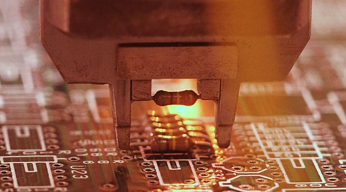
ISMI Industry Productivity Driver
|
|
|
- Barrie Wheeler
- 6 years ago
- Views:
Transcription


1 SEMATECH Symposium Japan September 15, 2010 Accelerating Manufacturing Productivity ISMI Industry Productivity Driver Scott Kramer VP Manufacturing Technology SEMATECH Copyright 2010 SEMATECH, Inc. SEMATECH, and the SEMATECH logo are registered servicemarks of SEMATECH, Inc. International SEMATECH Manufacturing Initiative, ISMI, Advanced Materials Research Center and AMRC are servicemarks of SEMATECH, Inc. All other servicemarks and trademarks are the property of their respective owners.
2 ISMI - Focus on semiconductor manufacturing productivity The productivity challenge How to determine, achieve, and maintain world class fab productivity How to increase productivity today and into the future The cost reduction challenge How to continuously reduce costs in today s fabs How to manage ever-increasing capital, manufacturing, and R&D costs The sustainability challenge How to reduce our environmental footprint Good for the environment, good for business 2


3 Manufacturing solutions to improve productivity and reduce cost Benchmarking and shared learning forums for continuous productivity improvement of existing factories and equipment Industry standards and guidelines for manufacturing excellence in next generation factories and equipment Environment, safety, and health technology for resource conservation and manufacturing sustainability Development and evaluation of applications for advanced metrology technology Realization of a cost-effective 450 mm transition SECS/GEM Port Control Interface A Port Data Councils and Forums Continuous Improvement Manufacturing Capabilities ESH Technology Metrology Technology 450 mm Transition 3

4 ISMI members 4
5 ISMI focus areas Mature Fabs Manufacturing Capabilities Program ESH Technology Center Metrology 450mm Transition Five operations councils Seven business Councils Fab productivity workshops Equipment productivity workshops (150mm, 200mm and 300mm) Alternate source spare parts Factory productivity improvement Factory cost analysis Enhanced equipment quality assurance Equipment performance improvement ESH global Strategies ESH resource Conservation ESH technology Environmental Research center (ERC) ESH advanced technology assessments Defect Metrology Lithography Metrology Films Metrology 450mm silicon readiness 450mm test wafer generation 450mm equipment demonstration 450mm ESH challenges 450mm factory readiness / ITB Manufacturing Excellence Installed based equipment forums 5
6 Mature Fabs 6
 Council Semiconductor Logistics Forum Equipment Procurement")
7 ISMI councils Manufacturing Methods Council Facilities Council Yield Council Operations Councils Wafer Probe Council Test Council Assembly - Package Council Critical Materials Council Reliability Council Quality Council Business Councils Statistics Council Failure Analysis (FA) Council Semiconductor Logistics Forum Equipment Procurement Council 7
8 ISMI councils Benchmarking: know where you stand Identify best-in-class Share best practices Communicate requirements to suppliers Percent Example: Facilities cost survey Allocated facilities spending as a percent of total fab operations spending Member Fabs Surveyed 8
 March 2010 Ion Implant April 2010 CVD (single wafer) June 2010 Dry Etch July 2010 Litho (exposure) Sept 2010 Wet Process Sept 2010")
9 ISMI Equipment Productivity Forums A series of workshops - equipment suppliers, component suppliers, and fab equipment owners - collaborate to improve the productivity of installed base equipment 2010 Equipment Productivity Forums: Thermal (RTP and furnace) March 2010 Ion Implant April 2010 CVD (single wafer) June 2010 Dry Etch July 2010 Litho (exposure) Sept 2010 Wet Process Sept 2010 Metrology Oct 2010 PVD Oct 2010 CMP Nov 2010 Typical Equipment Productivity Forum agenda 9
10 ISMI Mature Fabs roadmap Current Fab Manufacturing Methods Operations cost reduction Equipment throughput Maintenance practices Facilities operations Quality Reliability Supply chain management Probe and test development Fab, probe and final test Yield Probe card Materials Logistics Supplier relations Statistics New Add new topic spaces for the mature fabs market: Manufacturing cost benchmarking Manufacturing Execution Systems (MES) and AEC/APC for mature fabs Automated Material Handling (AMHS) Broader OEM focus for equipment productivity improvements Non-Product Wafer (NPW) and engineering lot handling R&D management and manufacturability of new technologies Equipment alarms and message management 10
11 ESH Technology Center 11
12 ISMI - Focus on semiconductor manufacturing productivity The productivity challenge How to determine, achieve, and maintain world class fab productivity How to increase productivity today and into the future The cost reduction challenge How to continuously reduce costs in today s fabs How to manage ever-increasing capital, manufacturing, and R&D costs The sustainability challenge How to reduce our environmental footprint Good for the environment, good for business 12
 ESH technology")
13 ISMI ESH Technology Center Project areas ESH global strategies Understand impacts of current and emerging global ESH regulations Assist our industrial membership with response to global regulatory initiatives ESH resource conservation and manufacturing sustainability Reduce manufacturing environmental footprint Influence suppliers to reduce resources (energy, chemicals, water) ESH technology and assessments Emerging technologies assessments, e.g., EUV, TSV, nano-particles Greenhouse gas emissions University R&D on SC manufacturing sustainability, e.g., nano-particle exposure/toxicity 13
14 ISMI ESH Technology Center How we work Information meetings Technical projects Benchmarking and surveys Collaboration among IC makers Collaboration among IC makers and suppliers Develop guidelines and specifications University research ISMI ESH Technology Center Technical project presentations, workshop, and working group meetings Technical projects as requested by member companies Detailed surveys as requested by member companies Collaboration focused on technical projects Collaboration among IC makers, and equipment and materials suppliers on technical projects Guidelines, state of technology reports Industry guidance of University research for semiconductor sustainability 14
15 ISMI ESH Technology Center Component improvements 15

16 ISMI ESH Technology Center Fab-specific green building initiatives Green Fab Working Group established to apply green building principles to high tech manufacturing Fab-specific LEED workshops presented and online training developed Promotes adoption of fab-specific credits into the LEED rating system LEED Application guide for high tech facilities developed ISMI Member network currently includes 13 LEED projects, many others planned Texas Instruments RFAB, LEED Gold Certified 16
17 450 mm Transition 17

18 Wafer size the great cost equalizer 200mm 300mm 450mm ~ >2012 History shows that increasing wafer surface area by ~2.25X yields a 30% cost reduction and enables the inexpensively part of Moore s Law 18
19 ISMI 450 mm program mission and organization ISMI s 450 mm mission statement Enable a cost-effective 450 mm transition through coordination and development of infrastructure, guidance, and industry readiness ISMI 450 mm organization 450 mm transition program Supplier engagement Factory integration readiness Test wafer operations Starting materials Vacuum platform development Equipment test methods and metrics 19
20 450 mm progress 2009 thru 2010 Wafer Inventory Process and Metrology Equipment Factory Integration Standards and Guidelines Jul-2009 Single crystal wafers available for development 1 st 450 mm equipment ordered Multiple carriers, loadports and EFEMS in testing. Mech. Wfr standard passed Jul-2010 ~440 wafers loaned to 25 suppliers 450mm Particle inspection, wafer edge inspection, wet cleaning, lot sorter, and ellipsometer equipment installed and operational Experiments started for thermal oxidation and oxide deposition/etch. 450 mm EHS Guidelines Defined 450 mm Factory Integration is reasonably mature ISMI ITB is nearing completion AMHS pilot lines exist, and are under evaluation FOUP and Loadport standards completed Developmental wafer Standard completed 20
21 ISMI s unique value proposition Members determine programs and deliverables Industry wide benchmarking Critical mass of industry participants Provides a legal safe haven for competitive benchmarking Tried and true methods and procedures Facilitate shared learning Group discussions produce new and best known methods Learn from another company's ingenuity Share business process methodologies and approaches Secure member website for 24/7 IP access Peer networking Create structured interactions for value creation Industry experts Key industry supply base 21
22 SEMATECH/ISMI model for participation SEMATECH membership Members participate in all programs ISMI membership International SEMATECH Manufacturing Initiative Members participate only in manufacturing programs Program membership Members participate in individual programs Membership open to chipmakers and equipment/material suppliers Project/council membership Members participate in individual projects or business councils Supplier participate by invitation in council and workshop sessions 22
23 Summary ISMI is an industry driver for productivity Cost reduction Productivity improvement Projects cover all facets of semiconductor manufacturing Many ways to participate join us! 23


24 Accelerating the next technology revolution Research Development Manufacturing 24
ISMI 450mm Transition Program
 SEMATECH Symposium Japan September 15, 2010 Accelerating Manufacturing Productivity ISMI 450mm Transition Program Scott Kramer VP Manufacturing Technology SEMATECH Copyright 2010 SEMATECH, Inc. SEMATECH,
ISMI 450mm Transition Program
 SEMATECH Symposium Taiwan September 7, 2010 Accelerating Manufacturing Productivity ISMI 450mm Transition Program Scott Kramer VP Manufacturing Technology SEMATECH Copyright 2010 SEMATECH, Inc. SEMATECH,
The SEMATECH Model: Potential Applications to PV
 Continually cited as the model for a successful industry/government consortium Accelerating the next technology revolution The SEMATECH Model: Potential Applications to PV Dr. Michael R. Polcari President
450mm silicon wafers specification challenges. Mike Goldstein Intel Corp.
 450mm silicon wafers specification challenges Mike Goldstein Intel Corp. Outline Background 450mm transition program 450mm silicon evolution Mechanical grade wafers (spec case study) Developmental (test)
Lithography Industry Collaborations
 Accelerating the next technology revolution Lithography Industry Collaborations SOKUDO Breakfast July 13, 2011 Stefan Wurm SEMATECH Copyright 2009 SEMATECH, Inc. SEMATECH, and the SEMATECH logo are registered
G450C. Global 450mm Consortium at CNSE. Michael Liehr, General Manager G450C, Vice President for Research
 Global 450mm Consortium at CNSE Michael Liehr, General Manager G450C, Vice President for Research - CNSE Overview - G450C Vision - G450C Mission - Org Structure - Scope - Timeline The Road Ahead for Nano-Fabrication
ISMI 450 mm Industry Briefing
 Accelerating Manufacturing Productivity ISMI 450 mm Industry Briefing July 15th, 2009 SEMICON West Copyright 2009 SEMATECH, Inc. SEMATECH, and the SEMATECH logo are registered servicemarks of SEMATECH,
Accelerating Growth and Cost Reduction in the PV Industry
 Accelerating Growth and Cost Reduction in the PV Industry PV Technology Roadmaps and Industry Standards An Association s Approach Bettina Weiss / SEMI PV Group July 29, 2009 SEMI : The Global Association
Property right statement: Copyright of charts, tables and sentences in this report belongs to
 The Vertical Portal for China Business Intelligence. Semiconductor Equipment Industry Report, 2009 Nov/2009 Property right statement: Copyright of charts, tables and sentences in this report belongs to
It s Time for 300mm Prime
 It s Time for 300mm Prime Iddo Hadar Managing Director, 300mm Prime Program Office SEMI Strategic Business Conference Napa Valley, California Tuesday, April 24, 2007 Safe Harbor Statement This presentation
Advancing Industry Productivity
 Advancing Industry Productivity Iddo Hadar Joint Productivity Working Group Session Austin, Texas Thursday, October 12, 2006 F O U N D A T I O N E N G I N E E R I N G G R O U P Safe Harbor Statement This
Competitive in Mainstream Products
 Competitive in Mainstream Products Bert Koek VP, Business Unit manager 300mm Fabs Analyst Day 20 September 2005 ASML Competitive in mainstream products Introduction Market share Device layers critical
The Development of the Semiconductor CVD and ALD Requirement
 The Development of the Semiconductor CVD and ALD Requirement 1 Linx Consulting 1. We create knowledge and develop unique insights at the intersection of electronic thin film processes and the chemicals
Growing the Semiconductor Industry in New York: Challenges and Opportunities
 Accelerating the next technology revolution The SEMATECH New York Experience Growing the Semiconductor Industry in New York: Challenges and Opportunities Dan Armbrust President and CEO, SEMATECH April
A Perspective on Semiconductor Equipment. R. B. Herring March 4, 2004
 A Perspective on Semiconductor Equipment R. B. Herring March 4, 2004 Outline Semiconductor Industry Overview of circuit fabrication Semiconductor Equipment Industry Some equipment business strategies Product
Manufacturing Case Studies: Copy Exactly (CE!) and the two-year cycle at Intel
 and the two-year cycle at Intel") Manufacturing Case Studies: Copy Exactly (CE!) and the two-year cycle at Intel Paolo A. Gargini Director Technology Strategy Intel Fellow 1 Agenda 2-year cycle Copy Exactly Conclusions 2 I see no reason
Manufacturing Case Studies: Copy Exactly (CE!) and the two-year cycle at Intel Paolo A. Gargini Director Technology Strategy Intel Fellow 1 Agenda 2-year cycle Copy Exactly Conclusions 2 I see no reason
Public. Introduction to ASML. Ron Kool. SVP Corporate Strategy and Marketing. March-2015 Veldhoven
 Public Introduction to ASML Ron Kool SVP Corporate Strategy and Marketing March-2015 Veldhoven 1991 1992 1993 1994 1995 1996 1997 1998 1999 2000 2001 2002 2003 2004 2005 2006 2007 2008 2009 2010 2011 2012
450mm and Moore s Law Advanced Packaging Challenges and the Impact of 3D
 450mm and Moore s Law Advanced Packaging Challenges and the Impact of 3D Doug Anberg VP, Technical Marketing Ultratech SOKUDO Lithography Breakfast Forum July 10, 2013 Agenda Next Generation Technology
21 st Annual Needham Growth Conference
 21 st Annual Needham Growth Conference Investor Presentation January 15, 2019 Safe Harbor Statement The information contained in and discussed during this presentation may include forward-looking statements
Brussels 18/12/2018. Level(s) pilot project Experience Center in Slovenia Vincent Briard, Sustainability and Product Regulatory Affairs Director
 pilot project Experience Center in Slovenia Vincent Briard, Sustainability and Product Regulatory Affairs Director") Brussels 18/12/2018 Level(s) pilot project Experience Center in Slovenia Vincent Briard, Sustainability and Product Regulatory Affairs Director Knauf Insulation supports Level(s) Part of Knauf Insulation
Brussels 18/12/2018 Level(s) pilot project Experience Center in Slovenia Vincent Briard, Sustainability and Product Regulatory Affairs Director Knauf Insulation supports Level(s) Part of Knauf Insulation
From Possible to Practical The Evolution of Nanoimprint for Patterned Media
 From Possible to Practical The Evolution of Nanoimprint for Patterned Media Paul Hofemann March 13, 2009 HDD Areal Density Industry Roadmap 10,000 Media Technology Roadmap Today Areal Density (Gbit/in
26 June 2013 copyright 2013 G450C
 450 mm Equipment Demonstrations at G450C Statistics Used During Tests of the Semiconductor Industry s Latest Fab Equipment Transition Lorn Christal, G450C Program Manager Demonstration Test Execution 26
CMOS Digital Integrated Circuits Lec 2 Fabrication of MOSFETs
 CMOS Digital Integrated Circuits Lec 2 Fabrication of MOSFETs 1 CMOS Digital Integrated Circuits 3 rd Edition Categories of Materials Materials can be categorized into three main groups regarding their
Economic Model Workshop, Philadelphia
 Economic Model Workshop, Philadelphia Denis Fandel, Project Manager, MM&P 1 August 2001 Meeting Guidelines Project Mission / Model Overview Early Production Test Program Fundamental Assumption Allocation
W ith development risk fully borne by the equipment industry and a two-year delay in the main
 Page 1 of 5 Economic Challenges and Opportunities in the 300 mm Transition Iddo Hadar, Jaim Nulman, Kunio Achiwa, and Oded Turbahn, Applied Materials Inc. -- 10/1/1998 Semiconductor International W ith
2010 IRI Annual Meeting R&D in Transition
 2010 IRI Annual Meeting R&D in Transition U.S. Semiconductor R&D in Transition Dr. Peter J. Zdebel Senior VP and CTO ON Semiconductor May 4, 2010 Some Semiconductor Industry Facts Founded in the U.S. approximately
Collaboration: The Semiconductor Industry s Path to Survival and Growth
 Collaboration: The Semiconductor Industry s Path to Survival and Growth Dr. Michael R. Polcari President and CEO SEMATECH 15 March 2005 3/17/2005 J:\ADMCTR\OCE\M_Polcari\ITPC 10-04 1 Outline Environment
SEMATECH Defect Printability Studies
 Accelerating the next technology revolution SEMATECH Defect Printability Studies Il Yong Jang 1, Jenah Harris-Jones 1, Ranganath Teki 1, Vibhu Jindal 1, Frank Goodwin 1 Masaki Satake 2, Ying Li 2, Danping
ACCELERATING THE FUTURE OF SEMICONDUCTORS
 ACCELERATING THE FUTURE OF SEMICONDUCTORS 14 PRODUCTION FACILITIES 7R&D FACILITIES 10+ COUNTRIES VERSUM MATERIALS BY THE NUMBERS* *Fiscal year ending September 30, 2018. 250+ CUSTOMERS CORE INDUSTRIES
The Value of Membership.
 The Value of Membership. Driving the global transformation to a smarter, more sustainable world with digital solutions at its core. 2018 gesi.org Information and Communications Technology (ICT) innovators
Common Development Topics for Semiconductor Manufacturers and their Suppliers in Germany
 Common Development Topics for Semiconductor Manufacturers and their Suppliers in Germany SEMICON Europa 2013 TechARENA 1: Secondary Equipment Session Contact: Dr.-Ing. Martin Schellenberger, Fraunhofer
Semiconductor Process Diagnosis and Prognosis for DSfM
 Semiconductor Process Diagnosis and Prognosis for DSfM Department of Electronic Engineering Prof. Sang Jeen Hong Nov. 19, 2014 1/2 Agenda 1. Semiconductor Manufacturing Industry 2. Roles of Semiconductor
Intel Technology Journal
 Volume 06 Issue 02 Published, May 16, 2002 ISSN 1535766X Intel Technology Journal Semiconductor Technology and Manufacturing The Intel Lithography Roadmap A compiled version of all papers from this issue
Technology Transfers Opportunities, Process and Risk Mitigation. Radhika Srinivasan, Ph.D. IBM
 Technology Transfers Opportunities, Process and Risk Mitigation Radhika Srinivasan, Ph.D. IBM Abstract Technology Transfer is quintessential to any technology installation or semiconductor fab bring up.
Emerging Transportation Technology Strategic Plan for the St. Louis Region Project Summary June 28, 2017
 Emerging Transportation Technology Strategic Plan for the St. Louis Region Project Summary June 28, 2017 Prepared for: East West Gateway Council of Governments Background. Motivation Process to Create
Photoresists & Ancillaries. Materials for Semiconductor Manufacturing A TECHCET Critical Materials Report
 2018-19 Photoresists & Ancillaries Materials for Semiconductor Manufacturing A TECHCET Critical Materials Report Prepared by Ed Korczynski Reviewed and Edited by Lita Shon-Roy TECHCET CA LLC PO Box 3814
UV Nanoimprint Stepper Technology: Status and Roadmap. S.V. Sreenivasan Sematech Litho Forum May 14 th, 2008
 UV Nanoimprint Stepper Technology: Status and Roadmap S.V. Sreenivasan Sematech Litho Forum May 14 th, 2008 Overview Introduction Stepper technology status: Patterning and CD Control Through Etch Alignment
TWINSCAN XT:1950i Water-based immersion taken to the max Enabling fast, single-exposure lithography at sub 40 nm
 TWINSCAN XT:1950i Water-based immersion taken to the max Enabling fast, single-exposure lithography at sub 40 nm SEMICON West, San Francisco July 14-18, 2008 Slide 1 The immersion pool becomes an ocean
Doug Dunn ASML President and Chief Executive Officer Deutsche Bank Conference London, England September 19, / Slide 1
 Doug Dunn ASML President and Chief Executive Officer Deutsche Bank Conference London, England September 19, 2003 / Slide 1 Safe Harbor Safe Harbor Statement under the U.S. Private Securities Litigation
State of the art EUV mask blank inspection with a Lasertec M7360 at the SEMATECH MBDC
 State of the art EUV mask blank inspection with a Lasertec M7360 at the SEMATECH MBDC Patrick Kearney a, Won-Il Cho a, Chan-Uk Jeon a, Eric Gullikson b, Anwei Jia c, Tomoya Tamura c, Atsushi Tajima c,
ITRS Update (and the European situation) Mart Graef Delft University of Technology
 Mart Graef Delft University of Technology") ITRS Update (and the European situation) Mart Graef Delft University of Technology Overview Roadmapping: Moore s Law & More than Moore Europe and the Roadmap Beyond CMOS: Nano-Tec Infrastructures: ENI2
ITRS Update (and the European situation) Mart Graef Delft University of Technology Overview Roadmapping: Moore s Law & More than Moore Europe and the Roadmap Beyond CMOS: Nano-Tec Infrastructures: ENI2
Energy beam processing and the drive for ultra precision manufacturing
 Energy beam processing and the drive for ultra precision manufacturing An Exploration of Future Manufacturing Technologies in Response to the Increasing Demands and Complexity of Next Generation Smart
Guidelines to Promote National Integrated Circuit Industry Development : Unofficial Translation
 Guidelines to Promote National Integrated Circuit Industry Development : Unofficial Translation Ministry of Industry and Information Technology National Development and Reform Commission Ministry of Finance
International Collaboration Tools for Industrial Development
 International Collaboration Tools for Industrial Development 6 th CSIR Conference 5-6 October, 2017 Dan Nagy Managing Director IMS International dnagy@ims.org U.S. DEPARTMENT OF COMMERCE (NIST) 28 Countries
A Presentation to the National Academies July 29, Larry W. Sumney President/CEO Semiconductor Research Corporation1
 A Presentation to the National Academies July 29, 2009 Larry W. Sumney President/CEO Semiconductor Research Corporation1 What is SRC? World s leading consortium funding collaborative university research
Bank of America Merrill Lynch Taiwan, Technology and Beyond Conference
 Bank of America Merrill Lynch Taiwan, Technology and Beyond Conference Craig De Young Vice President Investor Relations Taipei, Taiwan March 12, 2013 Forward looking statements Slide 2 Safe Harbor Statement
Innovative Approaches in Collaborative Planning
 Innovative Approaches in Collaborative Planning Lessons Learned from Public and Private Sector Roadmaps Jack Eisenhauer Senior Vice President September 17, 2009 Ross Brindle Program Director Energetics
Turning the wheels of your success
 INDUSTRIAL SERVICES Turning the wheels of your success A comprehensive package of integrated services combining traditional certification and inspection with innovative business solutions based on the
IMPACT OF 450MM ON CMP
 IMPACT OF 450MM ON CMP MICHAEL CORBETT MANAGING PARTNER LINX CONSULTING, LLC MCORBETT@LINX-CONSULTING.COM PREPARED FOR CMPUG JULY 2011 LINX CONSULTING Outline 1. Overview of Linx Consulting 2. CMP Outlook/Drivers
AN ANALYSIS: TRADITIONAL SEMICONDUCTOR LITHOGRAPHY VERSUS EMERGING TECHNOLOGY (NANO IMPRINT) Robert L. Wright Kranthi Mitra Adusumilli
 Robert L. Wright Kranthi Mitra Adusumilli") Proceedings of the 2005 Winter Simulation Conference M. E. Kuhl, N. M. Steiger, F. B. Armstrong, and J. A. Joines, eds. AN ANALYSIS: TRADITIONAL SEMICONDUCTOR LITHOGRAPHY VERSUS EMERGING TECHNOLOGY (NANO
Proceedings of the 2005 Winter Simulation Conference M. E. Kuhl, N. M. Steiger, F. B. Armstrong, and J. A. Joines, eds. AN ANALYSIS: TRADITIONAL SEMICONDUCTOR LITHOGRAPHY VERSUS EMERGING TECHNOLOGY (NANO
Wireless Metrology in Semiconductor Manufacturing
 1 Wireless Metrology in Semiconductor Manufacturing Costas J. Spanos Seminar 2 Outline Historical perspective Hardware and software applications Breakthroughs that have yet to be realized Distributed control
EMERGING SUBSTRATE TECHNOLOGIES FOR PACKAGING
 EMERGING SUBSTRATE TECHNOLOGIES FOR PACKAGING Henry H. Utsunomiya Interconnection Technologies, Inc. Suwa City, Nagano Prefecture, Japan henryutsunomiya@mac.com ABSTRACT This presentation will outline
SPC Spring Meeting March 21, 2013
 SPC Spring Meeting March 21, 2013 A partnership to deliver the most current design guidance for packaging sustainability Adam Gendell, SPC Marina Pietrosel, ÉEQ Agenda Background of our collaborative project
Research Infrastructures and Innovation
 Research Infrastructures and Innovation Octavi Quintana Principal Adviser European Commission DG Research & Innovation The presentation shall neither be binding nor construed as constituting commitment
REWE Group Detox Program
 REWE Group Detox Program Status Report 2015 December 2015 Content 1. Introduction to the Detox Program Objective and Achievements REWE Group s Detox Program - Summary of Achievements The REWE Group Detox
The Collaboration Engine: Enabling Innovation in Microelectronics
 The Collaboration Engine: Enabling Innovation in Microelectronics Karen Savala President, SEMI Americas Outline About SEMI Semiconductors: A History of Collaboration Collaboration in other Microelectronics
Nanometer Technologies: Where Design and Manufacturing Converge. Walden C. Rhines CHAIRMAN & CEO
 Nanometer Technologies: Where Design and Manufacturing Converge Walden C. Rhines CHAIRMAN & CEO Nanometer Technologies: Where Design and Manufacturing Converge Nanometer technologies make designers aware
MAPPER: High throughput Maskless Lithography
 MAPPER: High throughput Maskless Lithography Marco Wieland CEA- Leti Alterative Lithography workshop 1 Today s agenda Introduction Applications Qualification of on-tool metrology by in-resist metrology
Proceedings. BiTS Shanghai October 21, Archive - Session BiTS Workshop Image: Zhu Difeng/Dollar Photo Club
 Proceedings Archive - Session 1 2015 BiTS Workshop Image: Zhu Difeng/Dollar Photo Club Proceedings With Thanks to Our Sponsors! Premier Honored Distinguished Publication Sponsor 2 Proceedings Presentation
(Complementary E-Beam Lithography)
") Extending Optical Lithography with C E B L (Complementary E-Beam Lithography) July 13, 2011 4008 Burton Drive, Santa Clara, CA 95054 Outline Complementary Lithography E-Beam Complements Optical Multibeam
Extending Optical Lithography with C E B L (Complementary E-Beam Lithography) July 13, 2011 4008 Burton Drive, Santa Clara, CA 95054 Outline Complementary Lithography E-Beam Complements Optical Multibeam
Wafer-Edge Challenges
 Wafer-Edge Challenges SEMI STEP Wafer Edge Profile SEMICON/West 2006 Tetsuo Fukuda SEMI Japan (Fujitsu) Japan Advanced Wafer Geometry Task Force SEMI Japan Abstract Issues on edge profile are discussed
Ministry of Industry. Indonesia s 4 th Industrial Revolution. Making Indonesia 4.0. Benchmarking Implementasi Industri 4.0 A.T.
 Ministry of Industry s 4 th Industrial Revolution Making 4.0 Benchmarking Implementasi Industri 4.0 A.T. Kearney Industry 4.0 initiative is the global trend in the manufacturing industry End of 18 th century
DTU DANCHIP an open access micro/nanofabrication facility bridging academic research and small scale production
 DTU DANCHIP an open access micro/nanofabrication facility bridging academic research and small scale production DTU Danchip National Center for Micro- and Nanofabrication DTU Danchip DTU Danchip is Denmark
THE WAFER FAB CLEANS IN SEMICONDUCTOR INDUSTRY FROM A MATERIALS SUPPLIER PERSPECTIVE
 THE WAFER FAB CLEANS IN SEMICONDUCTOR INDUSTRY FROM A MATERIALS SUPPLIER PERSPECTIVE Tianniu Rick Chen, Ph.D. General Manager SP&C Business (Surface Preparation & Cleans) OUTLINE Market drivers and challenges
SEMATECH A Final Report to the Department of Defense. February 21, 1997
 SEMATECH 1987--1997 A Final Report to the Department of Defense February 21, 1997 Executive Summary In 1987 the Defense Science Board Task Force on Semiconductor Dependency stated in its report that, "U.S.
SAMPLE SLIDES & COURSE OUTLINE. Core Competency In Semiconductor Technology: 2. FABRICATION. Dr. Theodore (Ted) Dellin
 Dellin") & Digging Deeper Devices, Fabrication & Reliability For More Info:.com or email Dellin@ieee.org SAMPLE SLIDES & COURSE OUTLINE In : 2. A Easy, Effective, of How Devices Are.. Recommended for everyone who
& Digging Deeper Devices, Fabrication & Reliability For More Info:.com or email Dellin@ieee.org SAMPLE SLIDES & COURSE OUTLINE In : 2. A Easy, Effective, of How Devices Are.. Recommended for everyone who
Nanomaterials: Applications, Implications and Safety Management in the SAICM Context Rob Visser
 Nanomaterials: Applications, Implications and Safety Management in the SAICM Context Rob Visser The Regulatory Challenge of Nanotechnology 20 January 2012 Bern, Switzerland 1 SAICM context: ICCM 2 considered
JTC1 Smart Ci,es workshop. Welcome!
 JTC1 Smart Ci,es workshop Welcome! British Standards smart cities programme Saviour Alfino, Project Manager Smart Cities Standards Strategy, BSI 2 nd September 2014 03/09/2014 Overview 1. Common city challenges
Delivering the Well Cost Reduction challenge
 Delivering the Well Cost Reduction challenge Delivering the well cost reduction challenge Who are Oil & Gas UK? Maximising economic recovery Well cost reduction Problem definition Business case Execution
6-7 October Marina Bay Sands Expo & Convention Centre Peony Ballroom [Level 4]
![6-7 October Marina Bay Sands Expo & Convention Centre Peony Ballroom [Level 4]](/thumbs/80/80853998.jpg "6-7 October Marina Bay Sands Expo & Convention Centre Peony Ballroom [Level 4]") camline http://www.camline.com Booth 22 camline s mission is to provide the highest quality software solutions for factory automation and logistics, helping global manufacturers maintain their competitive
camline http://www.camline.com Booth 22 camline s mission is to provide the highest quality software solutions for factory automation and logistics, helping global manufacturers maintain their competitive
Industry 4.0. Advanced and integrated SAFETY tools for tecnhical plants
 Industry 4.0 Advanced and integrated SAFETY tools for tecnhical plants Industry 4.0 Industry 4.0 is the digital transformation of manufacturing; leverages technologies, such as Big Data and Internet of
200mm and 300mm Test Patterned Wafers for Bonding Process Applications SKW ASSOCIATES, INC.
 C M P C h a r a c t e r I z a t I o n S o l u t I o n s 200mm and 300mm Test Patterned Wafers for Bonding Process Applications SKW ASSOCIATES, INC. 2920 Scott Blvd., Santa Clara, CA 95054 Tel: 408-919-0094,
Semiconductor Manufacturing Technology. Semiconductor Manufacturing Technology. Photolithography: Resist Development and Advanced Lithography
 Semiconductor Manufacturing Technology Michael Quirk & Julian Serda October 2001 by Prentice Hall Chapter 15 Photolithography: Resist Development and Advanced Lithography Eight Basic Steps of Photolithography
Smart Grid Maturity Model: A Vision for the Future of Smart Grid
 Smart Grid Maturity Model: A Vision for the Future of Smart Grid David W. White Smart Grid Maturity Model Project Manager White is a member of the Resilient Enterprise Management (REM) team in the CERT
Voltage Sag Immunity Compliance Certificate PULS QS10.241, QS A1, QS C1
 PSL File QS10_241 Last modified: 19 December 2011 PSL Power Standards Laboratory www.powerstandards.com 2020 Challenger Drive #100 Alameda, CA 94501 USA TEL ++1-510-522-4400 FAX ++1-510-522-4455 SEMI F47-0706
The Road to 450 mm Semiconductor Wafers Ira Feldman
 The Road to 450 mm Semiconductor Wafers Ira Feldman Feldman Engineering Corp. Why 450 mm Wafers? Technical Challenges Economic Challenges Solutions Summary Overview 2 the number of transistors on a chip
President Barack Obama The White House Washington, DC June 19, Dear Mr. President,
 President Barack Obama The White House Washington, DC 20502 June 19, 2014 Dear Mr. President, We are pleased to send you this report, which provides a summary of five regional workshops held across the
Acknowledgements. o Stephen Tobin. o Jason Malik. o Dr. Dragan Djurdjanovic. o Samsung Austin Semiconductor, Machine Learning
 Semicon West 2016 Acknowledgements o Stephen Tobin o Samsung Austin Semiconductor, Machine Learning o Jason Malik o Samsung Austin Semiconductor, Metrology o Dr. Dragan Djurdjanovic o University of Texas,
Mechatronics. Bring the challenge. We ll build the solution.
 Mechatronics Bring the challenge. We ll build the solution. VALUE-ADDED ENCODER ASSEMBLIES CUSTOMIZED ROTARY STAGES LINEAR AND CURVED STAGES VOICE COIL STAGES ROBOTIC JOINTS CUSTOMIZED ELECTRONICS, CABLING
Policy Partnership on Science, Technology and Innovation Strategic Plan ( ) (Endorsed)
 (Endorsed)") 2015/PPSTI2/004 Agenda Item: 9 Policy Partnership on Science, Technology and Innovation Strategic Plan (2016-2025) (Endorsed) Purpose: Consideration Submitted by: Chair 6 th Policy Partnership on Science,
2015/PPSTI2/004 Agenda Item: 9 Policy Partnership on Science, Technology and Innovation Strategic Plan (2016-2025) (Endorsed) Purpose: Consideration Submitted by: Chair 6 th Policy Partnership on Science,
Shandong Government Suggestions on Implementing New Document 4 to Speed up IC Industry Development
 Shandong Government Suggestions on Implementing New Document 4 to Speed up IC Industry Development Guiding Ideas, Basic Principles and Development Goals: 1. Guiding ideas: Implement plans and policies
Standardization in Horizon2020. Andreea Gulacsi, Unit Manager Research Integration CEN-CENELEC Management Centre
 Standardization in Horizon2020 Andreea Gulacsi, Unit Manager Research Integration CEN-CENELEC Management Centre Policy Context The Innovation Union, 2010: Standards play an important role for innovation
Mask Technology Development in Extreme-Ultraviolet Lithography
 Mask Technology Development in Extreme-Ultraviolet Lithography Anthony Yen September 6, 2013 Projected End of Optical Lithography 2013 TSMC, Ltd 1976 1979 1982 1985 1988 1991 1994 1997 2000 2003 2007 2012
CMP: Where have we been and where are we headed next? Robert L. Rhoades, Ph.D. NCCAVS CMPUG Meeting at Semicon West San Francisco, July 10, 2013
 CMP: Where have we been and where are we headed next? Robert L. Rhoades, Ph.D. NCCAVS CMPUG Meeting at Semicon West San Francisco, July 10, 2013 Outline Where have we been? Semiconductor Industry Birth
A European Perspective for Electronic Industry in Latin America
 A European Perspective for Electronic Industry in Latin America François Guibert Corporate Vice President, Emerging Markets Region General Manager Electronic, a Global World Security Networking Consumer
Top 50 Emerging Technologies & Growth Opportunities
 Top 50 Emerging Technologies & Growth Opportunities Multi-billion Dollar Technologies Ready to Energize Industries and Transform our World THE VALUE PROPOSITION TechVision s annual Top 50 Emerging Technologies
Bridges to the Future
 FOURTH EDITION 1 9 8 7 2 0 0 7 report Accelerating the next technology revolution In this edition: Bridges to the Future Why industry collaboration on technology innovation and manufacturing productivity
FOREST PRODUCTS: THE SHIFT TO DIGITAL ACCELERATES
 FOREST PRODUCTS: THE SHIFT TO DIGITAL ACCELERATES INTRODUCTION While the digital revolution has transformed many industries, its impact on forest products companies has been relatively limited, as the
Technology Evaluation. David A. Berg Queen s University Kingston, ON November 28, 2017
 Technology Evaluation David A. Berg Queen s University Kingston, ON November 28, 2017 About me Born and raised in Alberta Queen s alumni (as well as University of Calgary & Western) Recently retired from
Clients and Users in Construction. Research Roadmap Summary
 P a ic bl u on ti 8 0 4 Clients and Users in Construction Research Roadmap Summary CIB Roadmap.indd 1 26-05-2016 11:18:57 2 CIB Roadmap.indd 2 Title Subtitle Serial title Year Authors Language Pages Keywords
EXECUTIVE SUMMARY. St. Louis Region Emerging Transportation Technology Strategic Plan. June East-West Gateway Council of Governments ICF
 EXECUTIVE SUMMARY St. Louis Region Emerging Transportation Technology Strategic Plan June 2017 Prepared for East-West Gateway Council of Governments by ICF Introduction 1 ACKNOWLEDGEMENTS This document
Industrial Innovation Information Days Brussels 3-4 October 2017
 Industrial Innovation Information Days Brussels 3-4 October 2017 NMBP Programme 2018 TOPICS FACTORIES OF THE FUTURE (FOF) DG RTD & DG CNECT DT-FOF-05-2019: Open Innovation for collaborative production
FIATECH s Capital Projects Technology Roadmap: how we can use it today
 FIATECH s Capital Projects Technology Roadmap: how we can use it today Ric Jackson Director The FIATECH Consortium National Streamlining Conference Washington, DC February 15-16, 2006 FIATECH Industry-led,
Hiding In Plain Sight. How Ultrasonics Can Help You Find the Smallest Bonded Wafer and Device Defects. A Sonix White Paper
 Hiding In Plain Sight How Ultrasonics Can Help You Find the Smallest Bonded Wafer and Device Defects A Sonix White Paper If You Can See It, You Can Solve It: Understanding Ultrasonic Inspection of Bonded
Improving Safety Culture and Systems at Americas Ports
 June 8, 2011 Improving Safety Culture and Systems at Americas Ports Improving Safety Plan for the Future Pete M. Diana Project Manager Copyright 2011 DuPont. All rights reserved. The DuPont Oval Logo,
Fabricating 2.5D, 3D, 5.5D Devices
 Fabricating 2.5D, 3D, 5.5D Devices Bob Patti, CTO rpatti@tezzaron.com Tezzar on Semiconduct or 04/15/2013 1 Gen4 Dis-Integrated 3D Memory DRAM layers 42nm node 2 million vertical connections per lay per
Holistic Lithography. Christophe Fouquet. Executive Vice President, Applications. 24 November 2014
 Holistic Lithography Christophe Fouquet Executive Vice President, Applications 24 Holistic Lithography Introduction Customer Problem: Beyond 20nm node scanner and non scanner contributions must be addressed
BEYOND RoHS: EFFORTS TO STRENGTHEN THE ELECTRONICS MANUFACTURING SUPPLY CHAIN
 BEYOND RoHS: EFFORTS TO STRENGTHEN THE ELECTRONICS MANUFACTURING SUPPLY CHAIN 0 Robert C. Pfahl, Jr. International Electronics Manufacturing Initiative (inemi) Joe Johnson Cisco Systems, Inc Outline Introduction
Water, Energy and Environment in the scope of the Circular Economy
 Water, Energy and Environment in the scope of the Circular Economy Maria da Graça Carvalho 11th SDEWES Conference Lisbon 2016 Contents of the Presentation 1. The Circular Economy 2. The Horizon 2020 Program
Lithography. Development of High-Quality Attenuated Phase-Shift Masks
 Lithography S P E C I A L Development of High-Quality Attenuated Phase-Shift Masks by Toshihiro Ii and Masao Otaki, Toppan Printing Co., Ltd. Along with the year-by-year acceleration of semiconductor device