Des MEMS aux NEMS : évolution des technologies et des concepts aux travers des développements menés au LETI
|
|
|
- Suzan Cannon
- 5 years ago
- Views:
Transcription


1 Des MEMS aux NEMS : évolution des technologies et des concepts aux travers des développements menés au LETI Ph. Robert 1


2 Content LETI at a glance From MEMS to NEMS: 30 years of technological evolution MEMS/NEMS activity overview 2


3 Leti at a Glance R&D in Micro & Nano-technologies Applications Driven Technology Transfer Licensing CONSUMER AUTOMOTIVE SPACE & SCIENCE employees on LETI payroll SECURITY & SAFETY 260 M budget ~ 35 M CapEx ENERGY & ENVIRONMENT INDUSTRY & MEDICAL HEALTHCARE WIRELESS & SMART DEVICES > 275 new patents/year Portfolio > 1,700 patents 33 start-ups 3


4 Leti svalue Proposition - - Simple policy for IP Outstanding personnel - State-of-the-art research infrastructure Access to existing knowledge through technology platforms Our Mission: Create Innovation and Transfer it to Industry 4


5 A Complete Set of Research Platforms Nanotec 300 Advanced CMOS 200 MEMS 200 Nanoscale Characterization Integrative Industries Design Integrative Chemistry & Biology Photonics 5


6 Platforms MEMS 200 > 200 mm MEMS clean room capabilities 6


7 Content LETI at a glance From MEMS to NEMS: 30 years of technological evolution MEMS/NEMS activity overview 7
8 30 years background Thin Film Technology (Vacuum deposition through a shadow mask on glass wafer) Transfers Key dates Weight sensor year Hygrometer 8


9 30 years background Thin Film Technology Bulk Technology (Litho/ wet etching on Si or quartz wafer) Comb drive accelero patent Transfers Key dates Weight sensor Quartz accelerometer year Hygrometer High perf. pressure sensor


10 30 years background Thin Film Technology Bulk Technology Comb drive accelero patent Surface Technology (Litho/ DRIE on SOI or bonded wafers) Common lab. Transfers Key dates Weight sensor Quartz accelerometer 1996 Startup creation Pacemaker accelerometer Geophone year Inertial platform Hygrometer Miniature pressure sensor Far-IR µbolometer High perf. pressure sensor


 Leti/Caltech")


11 Transfers Key dates 30 years background Thin Film Technology Weight sensor Bulk Technology Comb drive accelero patent Surface Technology Quartz accelerometer 1996 Startup creation Pacemaker accelerometer Geophone Nano-scale Technology (DUV lithoon thin SOI) Leti/Caltech Alliance Common lab Startup creation year Inertial platform Hygrometer Miniature pressure sensor Far-IR µbolometer M&NEMS platform High perf. pressure sensor
12 Content LETI at a glance From MEMS to NEMS: 30 years of technological evolution MEMS/NEMS activity overview 31


13 From MEMS design to system integration 3D integration of heterogeneous functions 3D Integration & Prototyping Electronic Partitioning SD closed loop architectures ASIC manufacturing Physical & electrical charact. Reliability study Characterizations Packaging WLP, thin film cap, 3D Vacuum sealing Techno. Developments MEMS manufacturing MEMS 200 nm AlSi linewidth + K η = dkk 4 π f ( r 12 m 2 m 0 0, K, x ) = (1 r d Ω K 12 m 2 r e f ( r 12 m 2 2 x 12 m (1 e ) 2 2, K, x ) r 2 12 m x 2 ) 2 (1 Modelling & Simulation Analytical models Full simulation of MEMS LETI covers all these aspects 32 3


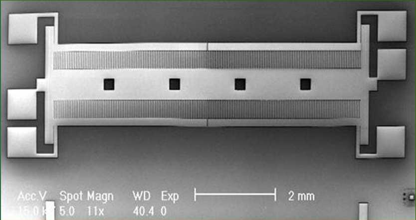
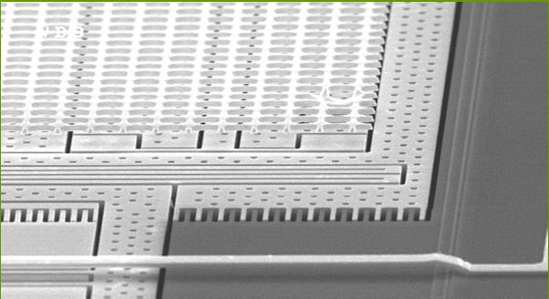
14 Expertise on Inertial Sensor 3D Gyro Accelerometer Geophone 33


15 Expertise on pressureand forcesensor Pressure sensor 560 µm cmut 3D Force sensor 34

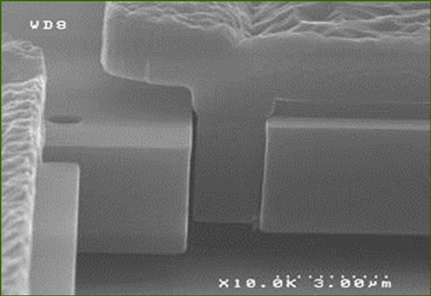
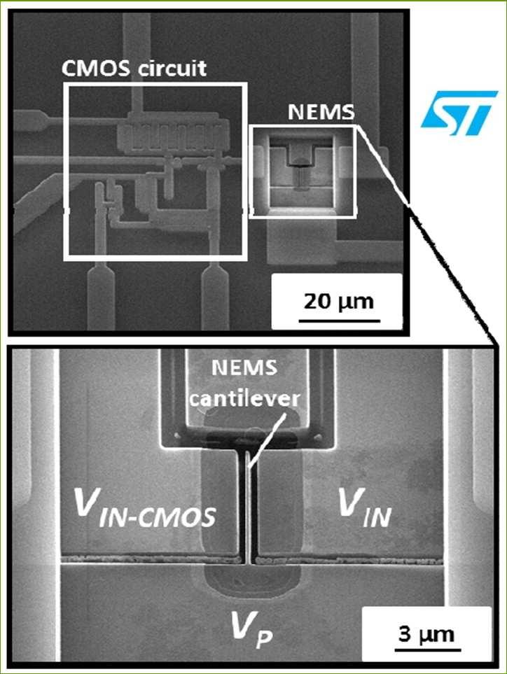
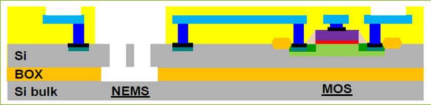
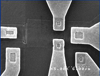
16 Expertise on Nano-Scale Sensors & Co-integration NEMS L= 1.6µm - ø~10nm 100 MHz / Q= CMOS Co-integration Nano gap (80nm) 35


17 Expertise on Bio-Chemical MEMS based Sensors µ-tof Mass-spec for NRBC gas detection Mass range targeted : 1Da 1.5 kda (1 Da=1.6x10⁻²⁴ g) NEMS-based chemical sensor Mass-spec for Biology applications Photo-acoustic chemical sensor Mass range targeted : 100 kda to 10 GDa (1 kda = 1.6x10⁻²¹ g) 1 nano particle (400 kda) detected 36


 110nm MEMS")
18 Expertise on Spintronics& MagneticSensors z Above-IC GMR current sensors contact y x Free layer Pinned layer H Current line Yoke width w Thickness of free layer t Magnetic Tunnel Junction (TMR, MRAM) 110nm MEMS Magnetometer 37


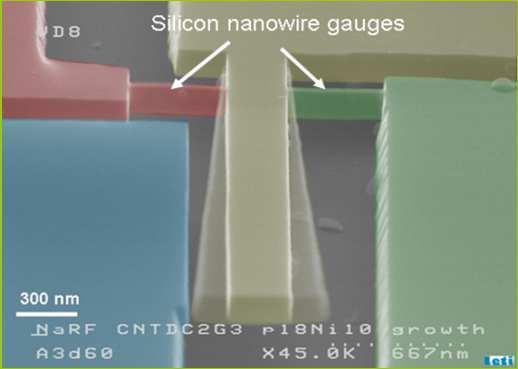
19 NEMS sensors platform Generic sensor platform based on resonantnems array detectors High efficiency patented NEMS resonator using : Electrostatic actuation Piezoresistive silicon nano-wire gauge Very high SNR Not sensitive to parasitic Suitable for high frequency application Low power consumption Well controlled technology compatible with DUV lithography Gas detection Mass-spec for Bio applications µbolometer Cellular force sensor 38


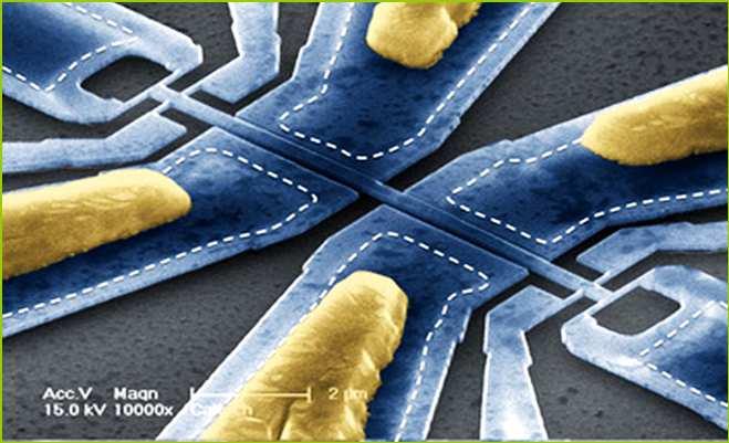
20 M&NEMS sensors platform Miniaturized sensors Generic platform sensors fusion + 1 common electronic MEMS size inertial mass + Nano-size piezoresistive gauge Not sensitive to parasitics An approach for low-power consumption + 15 patents 3D Accelero 3D gyro 3D magneto Microphone & Pressure sens. 39
Advancing MEMS R&D in materials, processes and devices to face major needs arising from the booming MEMS market
 Advancing MEMS R&D in materials, processes and devices to face major needs arising from the booming MEMS market Dr Julien Arcamone MEMS Business development Manager, CEA-LETI julien.arcamone@cea.fr MEMS
Plan Optik AG. Plan Optik AG PRODUCT CATALOGUE
 Plan Optik AG Plan Optik AG PRODUCT CATALOGUE 2 In order to service the high demand of wafers more quickly, Plan Optik provides off the shelf products in sizes from 2 up to 300mm diameter. Therefore Plan
MEMS Processes at CMP
 MEMS Processes at CMP MEMS Processes Bulk Micromachining MUMPs from MEMSCAP Teledyne DALSA MIDIS Micralyne MicraGEM-Si CEA/LETI Photonic Si-310 PHMP2M 2 Bulk micromachining on CMOS Compatible with electronics
DTU DANCHIP an open access micro/nanofabrication facility bridging academic research and small scale production
 DTU DANCHIP an open access micro/nanofabrication facility bridging academic research and small scale production DTU Danchip National Center for Micro- and Nanofabrication DTU Danchip DTU Danchip is Denmark
Recent Innovations in MEMS Sensors for PNT Applications
 Recent Innovations in MEMS Sensors for PNT Applications Stanford PNT Symposium 2017 Alissa M. Fitzgerald, Ph.D. Founder & CEO amf@amfitzgerald.com Overview Navigation Developments in MEMS gyroscope technology
Technology for the MEMS processing and testing environment. SUSS MicroTec AG Dr. Hans-Georg Kapitza
 Technology for the MEMS processing and testing environment SUSS MicroTec AG Dr. Hans-Georg Kapitza 1 SUSS MicroTec Industrial Group Founded 1949 as Karl Süss KG GmbH&Co. in Garching/ Munich San Jose Waterbury
Heterogeneous Technology Alliance. SOI MEMS Platform
 Heterogeneous Technology Alliance SOI MEMS Platform Added value of HTA SOI MEMS Platform to customers 23-Aug-11 Page 1 Attractive offering of HTA SOI MEMS Platform One-stop shop 1 Very extensive R&D resources,
MEMS in ECE at CMU. Gary K. Fedder
 MEMS in ECE at CMU Gary K. Fedder Department of Electrical and Computer Engineering and The Robotics Institute Carnegie Mellon University Pittsburgh, PA 15213-3890 fedder@ece.cmu.edu http://www.ece.cmu.edu/~mems
MEMS Sensors: From Automotive. CE Applications. MicroNanoTec Forum Innovations for Industry April 19 th Hannover, Germany
 MEMS Sensors: From Automotive to CE Applications MicroNanoTec Forum Innovations for Industry 2010 April 19 th Hannover, Germany Oliver Schatz, CTO 1 Engineering April 2010 GmbH 2009. All rights reserved,
MICROFLEX Project: MEMS on New Emerging Smart Textiles/Flexibles
 MICROFLEX Project: MEMS on New Emerging Smart Textiles/Flexibles S Beeby, M J Tudor, R Torah, K Yang, Y Wei Dr Steve Beeby ESD Research Group Smart Fabrics 2011 5 th April 2011 Overview Introduce the MicroFlex
Sensors and actuators at NXP: bringing more than Moore to CMOS
 Sensors and actuators at NXP: bringing more than Moore to CMOS Joost van Beek Senior Principal Scientist Corporate R&D, NXP Semiconductors Presented at the International Symposium on Advanced Hybrid Nano
DTU DANCHIP an open access micro/nanofabrication facility bridging academic research and small scale production
 DTU DANCHIP an open access micro/nanofabrication facility bridging academic research and small scale production DTU Danchip National Center for Micro- and Nanofabrication DTU Danchip DTU Danchip is Denmark
Micro and Smart Systems
 Micro and Smart Systems Lecture - 39 (1)Packaging Pressure sensors (Continued from Lecture 38) (2)Micromachined Silicon Accelerometers Prof K.N.Bhat, ECE Department, IISc Bangalore email: knbhat@gmail.com
Surface Micromachining
 Surface Micromachining An IC-Compatible Sensor Technology Bernhard E. Boser Berkeley Sensor & Actuator Center Dept. of Electrical Engineering and Computer Sciences University of California, Berkeley Sensor
Application-Based Opportunities for Reused Fab Lines
 Application-Based Opportunities for Reused Fab Lines Semicon China, March 17 th 2010 Keith Best Simax Lithography S I M A X A L L I A N C E P A R T N E R S Outline Market: Exciting More than Moore applications
Technology transfer and business development for innovation projects. From local market to global industry.
 Technology transfer and business development for innovation projects. From local market to global industry. www.zntc.ru Well positioned for innovative business development Fab и Lab R&D Multifunctional
CMUT and PMUT: New Technology Platform for Medical Ultrasound Rob van Schaijk
 CMUT and PMUT: New Technology Platform for Medical Ultrasound Rob van Schaijk November 2018 MUT introduction Medical ultra-sound imaging Probes and transducers Linear array Sound waves in straight line
MAPPER: High throughput Maskless Lithography
 MAPPER: High throughput Maskless Lithography Marco Wieland CEA- Leti Alterative Lithography workshop 1 Today s agenda Introduction Applications Qualification of on-tool metrology by in-resist metrology
RF DEVICES: BREAKTHROUGHS THANKS TO NEW MATERIALS. Jean-René Lequepeys. Leti Devices Workshop December 3, 2017
 RF DEVICES: BREAKTHROUGHS THANKS TO NEW MATERIALS Jean-René Lequepeys CELLULAR RF MARKETS RF cellular markets are still progressing Smartphones remain the main driver Declining growth rate but more complex
Faculty Development Program on Micro-Electro-Mechanical Systems (MEMS Sensor)
") Faculty Development Program on Micro-Electro-Mechanical Systems (MEMS Report MEMS sensors have been dominating the consumer products such as mobile phones, music players and other portable devices. With
Faculty Development Program on Micro-Electro-Mechanical Systems (MEMS Report MEMS sensors have been dominating the consumer products such as mobile phones, music players and other portable devices. With
SILICON BASED CAPACITIVE SENSORS FOR VIBRATION CONTROL
 SILICON BASED CAPACITIVE SENSORS FOR VIBRATION CONTROL Shailesh Kumar, A.K Meena, Monika Chaudhary & Amita Gupta* Solid State Physics Laboratory, Timarpur, Delhi-110054, India *Email: amita_gupta/sspl@ssplnet.org
National Centre for Flexible Electronics
 National Centre for Flexible Electronics Tripartite Partnership Government FlexE Centre - A platform for a meaningful interaction between industry and academia. An interdisciplinary team that advances
Feature-level Compensation & Control
 Feature-level Compensation & Control 2 Sensors and Control Nathan Cheung, Kameshwar Poolla, Costas Spanos Workshop 11/19/2003 3 Metrology, Control, and Integration Nathan Cheung, UCB SOI Wafers Multi wavelength
Si and InP Integration in the HELIOS project
 Si and InP Integration in the HELIOS project J.M. Fedeli CEA-LETI, Grenoble ( France) ECOC 2009 1 Basic information about HELIOS HELIOS photonics ELectronics functional Integration on CMOS www.helios-project.eu
Recent Developments in Multifunctional Integration. Stephan Guttowski, Head of Technology Park»Heterointegration«, Fraunhofer FMD
 Recent Developments in Multifunctional Integration Stephan Guttowski, Head of Technology Park»Heterointegration«, Fraunhofer FMD Founding Participants 2 One-Stop-Shop for developments from wafer technologies
Hermetic Packaging Solutions using Borosilicate Glass Thin Films. Lithoglas Hermetic Packaging Solutions using Borosilicate Glass Thin Films
 Hermetic Packaging Solutions using Borosilicate Glass Thin Films 1 Company Profile Company founded in 2006 ISO 9001:2008 qualified since 2011 Headquarters and Production in Dresden, Germany Production
End-of-line Standard Substrates For the Characterization of organic
 FRAUNHOFER INSTITUTe FoR Photonic Microsystems IPMS End-of-line Standard Substrates For the Characterization of organic semiconductor Materials Over the last few years, organic electronics have become
MEMS for RF, Micro Optics and Scanning Probe Nanotechnology Applications
 MEMS for RF, Micro Optics and Scanning Probe Nanotechnology Applications Part I: RF Applications Introductions and Motivations What are RF MEMS? Example Devices RFIC RFIC consists of Active components
1 Introduction 1.1 HISTORICAL DEVELOPMENT OF MICROELECTRONICS
 1 Introduction 1.1 HISTORICAL DEVELOPMENT OF MICROELECTRONICS The field of microelectronics began in 1948 when the first transistor was invented. This first transistor was a point-contact transistor, which
The 3D silicon leader. March 2012
 The 3D silicon leader March 2012 IPDiA overview Company located in Caen, Normandy, France Dedicated to manufacturing of integrated passive devices Employing 100 people and operating own wafer fab Strong
Micro-sensors - what happens when you make "classical" devices "small": MEMS devices and integrated bolometric IR detectors
 Micro-sensors - what happens when you make "classical" devices "small": MEMS devices and integrated bolometric IR detectors Dean P. Neikirk 1 MURI bio-ir sensors kick-off 6/16/98 Where are the targets
Low Energy Communication: NanoPhotonic & Electrical. Prof. Eli Yablonovitch EECS Dept. UC Berkeley
 Low Energy Communication: NanoPhotonic & Electrical Prof. Eli Yablonovitch EECS Dept. UC Berkeley What is the energy cost of reading out your flash memory? Read the current going through a resistor, in
Advanced PDK and Technologies accessible through ASCENT
 Advanced PDK and Technologies accessible through ASCENT MOS-AK Dresden, Sept. 3, 2018 L. Perniola*, O. Rozeau*, O. Faynot*, T. Poiroux*, P. Roseingrave^ olivier.faynot@cea.fr *Cea-Leti, Grenoble France;
2007-Novel structures of a MEMS-based pressure sensor
 C-(No.16 font) put by office 2007-Novel structures of a MEMS-based pressure sensor Chang-Sin Park(*1), Young-Soo Choi(*1), Dong-Weon Lee (*2) and Bo-Seon Kang(*2) (1*) Department of Mechanical Engineering,
BCD Smart Power Roadmap Trends and Challenges. Giuseppe Croce NEREID WORKSHOP Smart Energy Bertinoro, October 20 th
 BCD Smart Power Roadmap Trends and Challenges Giuseppe Croce NEREID WORKSHOP Smart Energy Bertinoro, October 20 th Outline 2 Introduction Major Trends in Smart Power ASICs An insight on (some) differentiating
Chapter 7 Introduction to 3D Integration Technology using TSV
 Chapter 7 Introduction to 3D Integration Technology using TSV Jin-Fu Li Department of Electrical Engineering National Central University Jungli, Taiwan Outline Why 3D Integration An Exemplary TSV Process
PROFILE CONTROL OF A BOROSILICATE-GLASS GROOVE FORMED BY DEEP REACTIVE ION ETCHING. Teruhisa Akashi and Yasuhiro Yoshimura
 Stresa, Italy, 25-27 April 2007 PROFILE CONTROL OF A BOROSILICATE-GLASS GROOVE FORMED BY DEEP REACTIVE ION ETCHING Teruhisa Akashi and Yasuhiro Yoshimura Mechanical Engineering Research Laboratory (MERL),
MEMS technologies and sensor examples for industry, mobility and smart environment
 MEMS technologies and sensor examples for industry, mobility and smart environment Karla Hiller, TU Chemnitz, Zentrum für Mikrotechnologien, Reichenhainer Str. 70, 09126 Chemnitz, karla.hiller@zfm.tu-chemnitz.de
Nanotechnology, the infrastructure, and IBM s research projects
 Nanotechnology, the infrastructure, and IBM s research projects Dr. Paul Seidler Coordinator Nanotechnology Center, IBM Research - Zurich Nanotechnology is the understanding and control of matter at dimensions
CMP for More Than Moore
 2009 Levitronix Conference on CMP Gerfried Zwicker Fraunhofer Institute for Silicon Technology ISIT Itzehoe, Germany gerfried.zwicker@isit.fraunhofer.de Contents Moore s Law and More Than Moore Comparison:
3D Integration developments & manufacturing CEA-LETI. D. Henry CEA-Leti-Minatec
 3D Integration developments & manufacturing offer @ CEA-LETI D. Henry CEA-Leti-Minatec Outline Introduction 3D Integration R&D activities overview 3D integration Manufacturing offer : Open 3D platform
Thermal Conductivity Sensor for Leak or Pressure Detection MTCS2601. MTCS2601 silicon sensing die in SMD ceramic package
 Sensor Description Thermal Conductivity Sensor for Leak or Pressure Detection MTCS2601 MTCS2601 silicon sensing die in SMD ceramic package Thermal conductivity sensor for primary vacuum measurement Silicon
ICU News Flash. ICU consortium. Infrared Imaging Components for Use in Automotive Safety Applications (ICU)
") We would welcome your opinion and comments at the contact option on ICU s website ICU News Flash Infrared Imaging Components for Use in Automotive Safety Applications (ICU) Co-financed by the EC D e a
We would welcome your opinion and comments at the contact option on ICU s website ICU News Flash Infrared Imaging Components for Use in Automotive Safety Applications (ICU) Co-financed by the EC D e a
MEDIA RELEASE FOR IMMEDIATE RELEASE 26 JULY 2016
 MEDIA RELEASE FOR IMMEDIATE RELEASE 26 JULY 2016 A*STAR S IME KICKS OFF CONSORTIA TO DEVELOP ADVANCED PACKAGING SOLUTIONS FOR NEXT-GENERATION INTERNET OF THINGS APPLICATIONS AND HIGH-PERFORMANCE WIRELESS
New Type of RF Switches for Signal Frequencies of up to 75 GHz
 New Type of RF Switches for Signal Frequencies of up to 75 GHz Steffen Kurth Fraunhofer ENAS, Chemnitz, Germany Page 1 Contents Introduction and motivation RF MEMS technology Design and simulation Test
MEMS Sensors as enablers for IoTS Shanghai, 17 th of March 2014 百里博 / Leopold Beer Regional President Asia Pacific
 - The MEMS Technology Leader MEMS Sensors as enablers for IoTS Shanghai, 17 th of March 2014 百里博 / Leopold Beer Regional President Asia Pacific 1 Marketing 17/03/2014 GmbH 2013. All rights reserved, also
Nanostencil Lithography and Nanoelectronic Applications
 Microsystems Laboratory Nanostencil Lithography and Nanoelectronic Applications Oscar Vazquez, Marc van den Boogaart, Dr. Lianne Doeswijk, Prof. Juergen Brugger, LMIS1 Dr. Chan Woo Park, Visiting Professor
Lithography in our Connected World
 Lithography in our Connected World SEMI Austin Spring Forum TOP PAN P R INTING CO., LTD MATER IAL SOLUTIONS DIVISION Toppan Printing Co., LTD A Broad-Based Global Printing Company Foundation: January 17,
MEMS Technology Roadmapping
 MEMS Technology Roadmapping Michael Gaitan, NIST Chair, inemi and ITRS MEMS Technology Working Groups Nano-Tec Workshop 3 31 May 2012 MEMS Technology Working Group More than Moore White Paper, http://www.itrs.net
Introduction to Microeletromechanical Systems (MEMS) Lecture 12 Topics. MEMS Overview
 Lecture 12 Topics. MEMS Overview") Introduction to Microeletromechanical Systems (MEMS) Lecture 2 Topics MEMS for Wireless Communication Components for Wireless Communication Mechanical/Electrical Systems Mechanical Resonators o Quality
Introduction to Microeletromechanical Systems (MEMS) Lecture 2 Topics MEMS for Wireless Communication Components for Wireless Communication Mechanical/Electrical Systems Mechanical Resonators o Quality
New Wave SiP solution for Power
 New Wave SiP solution for Power Vincent Lin Corporate R&D ASE Group APEC March 7 th, 2018 in San Antonio, Texas. 0 Outline Challenges Facing Human Society Energy, Environment and Traffic Autonomous Driving
TSI, or through-silicon insulation, is the
 Vertical through-wafer insulation: Enabling integration and innovation PETER HIMES, Silex Microsystems AB, Järfälla SWEDEN Through-wafer insulation has been used to develop technologies such as Sil-Via
Final Exam Topics. IC Technology Advancement. Microelectronics Technology in the 21 st Century. Intel s 90 nm CMOS Technology. 14 nm CMOS Transistors
 ANNOUNCEMENTS Final Exam: When: Wednesday 12/10 12:30-3:30PM Where: 10 Evans (last names beginning A-R) 60 Evans (last names beginning S-Z) Comprehensive coverage of course material Closed book; 3 sheets
Challenges in Imaging, Sensors, and Signal Processing
 Challenges in Imaging, Sensors, and Signal Processing Raymond Balcerak MTO Technology Symposium March 5-7, 2007 1 Report Documentation Page Form Approved OMB No. 0704-0188 Public reporting burden for the
Novel piezoresistive e-nose sensor array cell
 4M2007 Conference on Multi-Material Micro Manufacture 3-5 October 2007 Borovets Bulgaria Novel piezoresistive e-nose sensor array cell V.Stavrov a, P.Vitanov b, E.Tomerov a, E.Goranova b, G.Stavreva a
Industrialization of Micro-Electro-Mechanical Systems. Werner Weber Infineon Technologies
 Industrialization of Micro-Electro-Mechanical Systems Werner Weber Infineon Technologies Semiconductor-based MEMS market MEMS Market 2004 (total 22.7 BUS$) Others mostly Digital Light Projection IR Sensors
Body-Biased Complementary Logic Implemented Using AlN Piezoelectric MEMS Switches
 University of Pennsylvania From the SelectedWorks of Nipun Sinha 29 Body-Biased Complementary Logic Implemented Using AlN Piezoelectric MEMS Switches Nipun Sinha, University of Pennsylvania Timothy S.
Micro-PackS, Technology Platform. Security Characterization Lab Opening
 September, 30 th 2008 Micro-PackS, Technology Platform Security Characterization Lab Opening Members : Micro-PackS in SCS cluster From Silicium to innovative & commucating device R&D structure, gathering
Lecture: Integration of silicon photonics with electronics. Prepared by Jean-Marc FEDELI CEA-LETI
 Lecture: Integration of silicon photonics with electronics Prepared by Jean-Marc FEDELI CEA-LETI Context The goal is to give optical functionalities to electronics integrated circuit (EIC) The objectives
Low-Cost Far-Infrared FPA based on High-Volume Pressure Sensor Process
 Low-Cost Far-Infrared FPA based on High-Volume Pressure Sensor Process Michael Krueger 1, Ingo Herrmann 1 Robert Bosch GmbH - Automotive Electronics, Tuebinger Str. 13, D-776 Reutlingen, Germany, michael.krueger@de.bosch.com
ISSCC 2006 / SESSION 16 / MEMS AND SENSORS / 16.1
 16.1 A 4.5mW Closed-Loop Σ Micro-Gravity CMOS-SOI Accelerometer Babak Vakili Amini, Reza Abdolvand, Farrokh Ayazi Georgia Institute of Technology, Atlanta, GA Recently, there has been an increasing demand
AlN Contour-Mode Resonators for Narrow-Band Filters above 3 GHz
 From the SelectedWorks of Chengjie Zuo April, 2009 AlN Contour-Mode Resonators for Narrow-Band Filters above 3 GHz Matteo Rinaldi, University of Pennsylvania Chiara Zuniga, University of Pennsylvania Chengjie
Synthesis of Silicon. applications. Nanowires Team. Régis Rogel (Ass.Pr), Anne-Claire Salaün (Ass. Pr)
, Anne-Claire Salaün (Ass. Pr)") Synthesis of Silicon nanowires for sensor applications Anne-Claire Salaün Nanowires Team Laurent Pichon (Pr), Régis Rogel (Ass.Pr), Anne-Claire Salaün (Ass. Pr) Ph-D positions: Fouad Demami, Liang Ni,
Synthesis of Silicon nanowires for sensor applications Anne-Claire Salaün Nanowires Team Laurent Pichon (Pr), Régis Rogel (Ass.Pr), Anne-Claire Salaün (Ass. Pr) Ph-D positions: Fouad Demami, Liang Ni,
Academic Course Description SRM University Faculty of Engineering and Technology Department of Electronics and Communication Engineering
 Academic Course Description SRM University Faculty of Engineering and Technology Department of Electronics and Communication Engineering EC0032 Introduction to MEMS Eighth semester, 2014-15 (Even Semester)
Holst Centre Wireless Autonomous Sensor Technologies & Flexible Electronics
 February 10, 2011 Holst Centre Wireless Autonomous Sensor Technologies & Flexible Electronics Presentation overview -General overview -Research focus < 4 Holst Centre: a solid partner in research Independent,
Extending The Life Of 200mm Fabs And The Re-use of Second Hand Tools
 Extending The Life Of 200mm Fabs And The Re-use of Second Hand Tools Gareth Bignell, FE Equipment Procurement Director SEMICON Europa 2012 Presentation Summary 2 An introduction to STMicroelectronics The
Study of MEMS Devices for Space Applications ~Study Status and Subject of RF-MEMS~
 Study of MEMS Devices for Space Applications ~Study Status and Subject of RF-MEMS~ The 26 th Microelectronics Workshop October, 2013 Maya Kato Electronic Devices and Materials Group Japan Aerospace Exploration
Aluminum Nitride Reconfigurable RF-MEMS Front-Ends
 From the SelectedWorks of Chengjie Zuo October 2011 Aluminum Nitride Reconfigurable RF-MEMS Front-Ends Augusto Tazzoli University of Pennsylvania Matteo Rinaldi University of Pennsylvania Chengjie Zuo
IC1301 -WiPE. Wireless Power Transmission for Sustainable Electronics. SWG4.1: Space Applications. 25 March 2014
 IC1301 -WiPE Wireless Power Transmission for Sustainable Electronics SWG4.1: Space Applications 25 March 2014 Alexandru Takacs CNRS LAAS, Toulouse, France University of Toulouse III Paul Sabatier, France
ICT Micro- and nanoelectronics technologies
 EPoSS Proposers' Day, 2 Feb 2017, Brussels ICT 31-2017 Micro- and nanoelectronics technologies Eric Fribourg-Blanc, Henri Rajbenbach, Andreas Lymberis European Commission DG CONNECT (Communications Networks,
300mm BEOL manufacturing capabili=es in Russia. November 2017 CNE PROPRIETARY
 300mm BEOL manufacturing capabili=es in Russia November 2017 About CNE CNE is a pure-play 300mm BEOL Foundry with state of the art equipment, advanced process technologies and capabiliees Crocus Nano Electronics
RF MEMS Simulation High Isolation CPW Shunt Switches
 RF MEMS Simulation High Isolation CPW Shunt Switches Authored by: Desmond Tan James Chow Ansoft Corporation Ansoft 2003 / Global Seminars: Delivering Performance Presentation #4 What s MEMS Micro-Electro-Mechanical
Yoshihiko ISOBE Hiroshi MUTO Tsuyoshi FUKADA Seiji FUJINO
 Yoshihiko ISOBE Hiroshi MUTO Tsuyoshi FUKADA Seiji FUJINO Increased performance requirements in terms of the environment, safety and comfort have recently been imposed on automobiles to ensure efficient
High Frequency GaN-Based Power Conversion Stages
 PwSoC Cork 2008 High Frequency GaN-Based Power Conversion Stages Dr. Michael A. Briere ACOO Enterprises LLC 1 Anatomy of a power device driven revolution in power electronics Enabling Rapid Commercialization
EE C245 ME C218 Introduction to MEMS Design Fall 2007
 EE C245 ME C218 Introduction to MEMS Design Fall 2007 Prof. Clark T.-C. Nguyen Dept. of Electrical Engineering & Computer Sciences University of California at Berkeley Berkeley, CA 94720 Lecture 1: Definition
Noel Technologies. Provider of Advanced Lithography and Semiconductor Thin Film Services
 Noel Technologies Provider of Advanced Lithography and Semiconductor Thin Film Services Noel Technologies Keith Best Biography Over the last 27 years, Keith Best has held a variety of semiconductor processing
Micro-nanosystems for electrical metrology and precision instrumentation
 Micro-nanosystems for electrical metrology and precision instrumentation A. Bounouh 1, F. Blard 1,2, H. Camon 2, D. Bélières 1, F. Ziadé 1 1 LNE 29 avenue Roger Hennequin, 78197 Trappes, France, alexandre.bounouh@lne.fr
How material engineering contributes to delivering innovation in the hyper connected world
 How material engineering contributes to delivering innovation in the hyper connected world Paul BOUDRE, Soitec CEO Leti Innovation Days - July 2018 Grenoble, France We live in a world of data In perpetual
Design of MEMS Piezoelectric Vibrational Energy Harvesters for Industrial and Commercial Applications
 Design of MEMS Piezoelectric Vibrational Energy Harvesters for Industrial and Commercial Applications Consumer Applications Civil Infrastructure Kathleen M. Vaeth, Vice President of Engineering microgen
World s First Piezoelectric MEMS Oscillators
 World s First Piezoelectric MEMS Oscillators September 29 th 2012 Harmeet.Bhugra@idt.com Managing Director MEMS Division, IDT Inc. 2012 Integrated Device Technology, Inc. 1 Introduction to IDT Overview:
Nano-structured superconducting single-photon detector
 Nano-structured superconducting single-photon detector G. Gol'tsman *a, A. Korneev a,v. Izbenko a, K. Smirnov a, P. Kouminov a, B. Voronov a, A. Verevkin b, J. Zhang b, A. Pearlman b, W. Slysz b, and R.
Technology & Manufacturing
 Technology & Manufacturing Jean-Marc Chery Chief Operating Officer Front-End Manufacturing Unique capability 2 Technology portfolio aligned with application focus areas Flexible IDM model with foundry
EE C245 ME C218 Introduction to MEMS Design
 EE C245 ME C218 Introduction to MEMS Design Fall 2008 Prof. Clark T.-C. Nguyen Dept. of Electrical Engineering & Computer Sciences University of California at Berkeley Berkeley, CA 94720 Lecture 1: Definition
MEAS Silicon MEMS Piezoresistive Accelerometer and its Benefits
 MEAS Silicon MEMS Piezoresistive Accelerometer and its Benefits Piezoresistive Accelerometers 1. Bonded Strain Gage type (Gages bonded to metal seismic mass using epoxy) Undamped circa 1950 s Fluid (oil)
MEMS-based Micro Coriolis mass flow sensor
 MEMS-based Micro Coriolis mass flow sensor J. Haneveld 1, D.M. Brouwer 2,3, A. Mehendale 2,3, R. Zwikker 3, T.S.J. Lammerink 1, M.J. de Boer 1, and R.J. Wiegerink 1. 1 MESA+ Institute for Nanotechnology,
Glenn G. Daves. Director, Packaging Solutions Development Freescale Semiconductor, Inc.
 Glenn G. Daves Director, Packaging Solutions Development Freescale Semiconductor, Inc. Freescale, the Freescale logo, AltiVec, C-5, CodeTEST, CodeWarrior, ColdFire, C-Ware, t he Energy Efficient Solutions
GSM OPTICAL MONITORING FOR HIGH PRECISION THIN FILM DEPOSITION
 OPTICAL MONITORING FOR HIGH PRECISION THIN FILM DEPOSITION OPTICAL MONITORING TECHNOLOGIES ENABLING OUR NEW WORLD! - ACHIEVING MORE DEMANDING THIN FILM SPECIFICATIONS - DRIVING DOWN UNIT COSTS THE GSM1101
Emerging MEMS & Sensor Technologies to Watch: Alissa M. Fitzgerald, Ph.D., Founder & CEO Semicon West 2018
 Emerging MEMS & Sensor Technologies to Watch: 2018 Alissa M. Fitzgerald, Ph.D., Founder & CEO amf@amfitzgerald.com Outline About AMFitzgerald What emerging means in this presentation Emerging MEMS & sensor
New fabrication and packaging technologies for CMOS pixel sensors: closing gap between hybrid and monolithic
 New fabrication and packaging technologies for CMOS pixel sensors: closing gap between hybrid and monolithic Outline Short history of MAPS development at IPHC Results from TowerJazz CIS test sensor Ultra-thin
3D Integration of MEMS and CMOS via Cu-Cu Bonding with Simultaneous Formation of Electrical, Mechanical and Hermetic Bonds
 3D Integration of MEMS and CMOS via Cu-Cu Bonding with Simultaneous Formation of Electrical, Mechanical and Hermetic Bonds R. Nadipalli 1, J. Fan 1, K. H. Li 2,3, K. W. Wee 3, H. Yu 1, and C. S. Tan 1
True Three-Dimensional Interconnections
 True Three-Dimensional Interconnections Satoshi Yamamoto, 1 Hiroyuki Wakioka, 1 Osamu Nukaga, 1 Takanao Suzuki, 2 and Tatsuo Suemasu 1 As one of the next-generation through-hole interconnection (THI) technologies,
IMAGE SENSOR EVOLUTION AND ENABLING 3D TECHNOLOGIES
 Fig. 5: Scanning Electron Microscopy images (TOP view, 3D view, Zoome including all metal levels of the BSI imager structure. (dashed line shows bonding IMAGE SENSOR EVOLUTION AND ENABLING 3D TECHNOLOGIES
Reducing MEMS product development and commercialization time
 Reducing MEMS product development and commercialization time Introduction Fariborz Maseeh, Andrew Swiecki, Nora Finch IntelliSense Corporation 36 Jonspin Road, Wilmington MA 01887 www.intellisense.com
IEEE JOURNAL OF SELECTED TOPICS IN QUANTUM ELECTRONICS 2010 Silicon Photonic Circuits: On-CMOS Integration, Fiber Optical Coupling, and Packaging
 IEEE JOURNAL OF SELECTED TOPICS IN QUANTUM ELECTRONICS 2010 Silicon Photonic Circuits: On-CMOS Integration, Fiber Optical Coupling, and Packaging Christophe Kopp, St ephane Bernab e, Badhise Ben Bakir,
RF-MST Cluster Workshop, Potsdam, FP Go4TIME
 RF-MST Cluster Workshop, Potsdam, 01.07.13 FP7-257444 Go4TIME Go4Time Consortium Leading Quartz and MEMS European manufacturers Three research labs Two Universities David Ruffieux Go4Time Technical Manager
Performance Characterization Of A Simultaneous Positive and Negative Ion Detector For Mass Spectrometry Applications
 Performance Characterization Of A Simultaneous Positive and Negative Ion Detector For Mass Spectrometry Applications Bruce Laprade and Raymond Cochran Introduction Microchannel Plates (Figures 1) are parallel
SmartSenseCom Introduces Next Generation Seismic Sensor Systems
 SmartSenseCom Introduces Next Generation Seismic Sensor Systems Summary: SmartSenseCom, Inc. (SSC) has introduced the next generation in seismic sensing technology. SSC s systems use a unique optical sensing
The Advantages of Integrated MEMS to Enable the Internet of Moving Things
 The Advantages of Integrated MEMS to Enable the Internet of Moving Things January 2018 The availability of contextual information regarding motion is transforming several consumer device applications.
A Modular MEMS Accelerometer Concept
 A Modular MEMS Accelerometer Concept M. Brandl, F. Schrank, Ch. Fürböck, V. Kempe austriamicrosystems AG 1, A-8141 Unterpremstaetten, Austria A quasi-monolithic MEMS concept setting up a new family of
EE C245 ME C218 Introduction to MEMS Design Fall 2010
 Instructor: Prof. Clark T.-C. Nguyen EE C245 ME C218 Introduction to MEMS Design Fall 2010 Prof. Clark T.-C. Nguyen Dept. of Electrical Engineering & Computer Sciences University of California at Berkeley