Synthesis of Silicon. applications. Nanowires Team. Régis Rogel (Ass.Pr), Anne-Claire Salaün (Ass. Pr)
|
|
|
- Pearl Lawrence
- 6 years ago
- Views:
Transcription
1 Synthesis of Silicon nanowires for sensor applications Anne-Claire Salaün Nanowires Team Laurent Pichon (Pr), Régis Rogel (Ass.Pr), Anne-Claire Salaün (Ass. Pr) Ph-D positions: Fouad Demami, Liang Ni, Gertrude Godem-Wenga 1 CMC2 - November FRONTIER-2009, 25, Barcelona, Nov Spain29-Dec 3, 2009, Sendai, Japan

2 IETR - Institut d Electronique et de Télécommunications de Rennes FRANCE Rennes 2


3 IETR - Institut d Electronique et de Télécommunications de Rennes FRANCE Microelectronics and Microsensors Department Two research teams involved Devices Development of process fabrication Microsensors Development of innovative sensors Research fields covered: Competences and know-how Micro/nano electronics Microtechnology/Microfluidic Sensors Microsystems and systems Electronic on plastic substrates Synthesis of Si related materials (thin films, nano-objects) Si & Ge low temperature technology on flexible substrate Actuation and detection techniques Chemical and biological detection 3
4 Introduction Context Owing to their physical and electrical properties, silicon nanowires represent a promising material with strong potential large variety of applications in future nanoelectronic devices Fabrication of innovative devices based on silicon nanowires with remarkable electronic properties. New topic in the lab Our objectives Synthesis of silicon nanowires Study and optimization of their electrical performances Fabrication of electronic devices (resistors, field-effect transistors) Development of innovative micro-sensors (chemical, biological) 4
5 Silicon nanowires Benefits of silicon nanowires (SiNWs) High surface / volume ratio: surface phenomena predominate Possibility of surface functionalization for biological applications Development of nanosensors with high sensitivity Compatibility with CMOS technologies Silicon nanowires synthesis: 2 approaches Top-down Approach Bottom-up Approach Starts from bulk materials and scales down the patterned areas Growth technique from molecular precursors using nanoparticles as catalysts t Optical and x-ray lithography E-beam and ion-beam lithography Scanning probe lithographyh Printing and imprinting Layer-by-layer self assembly Molecular self assembly Direct assembly Coating and growth 5
6 Outline Introduction Context Benefits of silicon nanowires (SiNWs) Silicon nanowires: bottom-up approach Synthesis method Fabrication of silicon nanowires based resistors Electrical l characterization ti Chemical species detection Silicon nanowires: top-down approach Synthesis method Fabrication of silicon nanowires based resistors Fabrication of nanowires Thin Film Transistors (SiNW-TFT) Electrical characterization Chemical species detection 6
7 SiNW synthesis : Bottom-up Bottom-up approach Nanowire synthesis is achieved by a vapor-liquid-solid (VLS) process A droplet of a liquid catalyst is put in contact with gaseous precursor molecules. SiNWs are synthesized using gold (Au) as metal catalyst and silane (SiH 4 ) as precursor gas in a hot wall LPCVD reactor. 7


 Diameter : about 100")
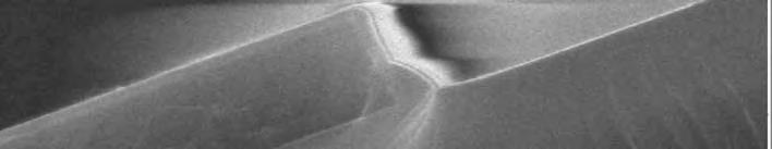
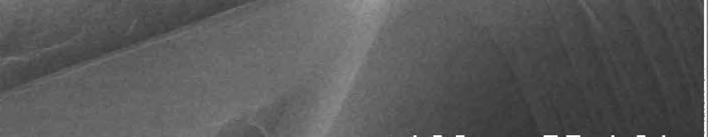
8 SiNW synthesis : Bottom-up The diameter of the nanowire, grown by the VLS process, is given by the diameter of the gold nanoparticles. Nanowire Au Gold deposited by thermal evaporation (thickness below 5 nm), Growth in LPCVD reactor with silane at 480 C (pressure: 40Pa) Diameter : about 100 nm, various orientation, length can exceed 10 µm 8
9 SiNW synthesis : Bottom-up Advantage of the VLS method: Possibility of selective doping (n- or p-type) of the nanowires, by controlled injection of the dopant precursor gas High quality single crystalline nanowires with well-controlled composition and electronic properties Challenges: Controlling diameter and orientation of the nanowires which impede the success of the fabrication of nanowire arrays with high degree of reproducibility. 9


10 Fabrication of nanowires based resistors SiNW synthesis : Bottom-up SiO 2 Highly in-situ doped polysilicon First mask Definition of the comb shape Electrodes geometry on a SiO 2 capped substrate Silicon substrate Au Second mask Thin film Au local deposition after lift-off technique nanowires Growth of SiNWs by LPCVD. Silicon nanowire network: used to interconnect electrodes Silicon substrate or glass substrate (maximum process temperature 600 C) 10

 0,0-5,0x10⁻⁹ 11-1,0x10⁻⁸ -1,0-0,5 0,0")
11 SiNW synthesis : Bottom-up Different interdigitated structures can be achieved, varying number of teeth and local deposition of gold 1,0x10⁻⁸ Au thickness : 5nm 5,0x10⁻⁹ Current (A) 0,0-5,0x ,0x ,0-0,5 0,0 0,5 1,0 Voltage (V)

12 SiNW synthesis : Bottom-up Thin Film Transistors with Nanowires Output characteristics 1,5x10⁻⁷ Source Drain 1,0x10⁻⁷ VG=10V ds I 5,0x10⁻⁸ VG=0V 0,0 VG=-20V Highly doped silicon substrate Gate Vds Field effect but bad electrical contact Surface sensitive to charges in ambiance 12
13 Silicon Nanowire as gas sensor SiNW synthesis : Bottom-up Main interest of SiNWs rests on their high surface that can be sensitive to charges SiNWs device exposed to smoke SiNWs device exposed to ammonia 1,0x10⁻⁷ smoke vacuum t (A) Current 8,0x10⁻⁸ 6,0x10⁻⁸ 4,0x10⁻⁸ air Reversible trend Resistan nce ( ) ,0x10-8 air 0, Time (sec) 21 min NH Time (min) ammonia and smoke may act as chemical gates: species act as electrons donor (reducing agents) at the SiNWs surface. positively charged gas molecules binded on SiNWs surface can modulate the conductance 13
14 Outline Introduction Context Benefits of silicon nanowires (SiNWs) Silicon nanowires: bottom-up approach Synthesis method Fabrication of silicon nanowires based resistors Electrical l characterization ti Chemical species detection Silicon nanowires: top-down approach Synthesis method Fabrication of silicon nanowires based resistors Fabrication of nanowires Thin Film Transistors (SiNW-TFT) Electrical characterization Chemical species detection 14
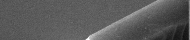
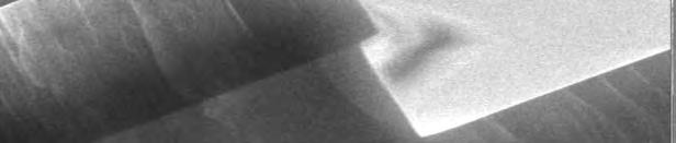
15 SiNW synthesis : Top-down Top-down approach starts from bulk materials and scales down the patterned areas Advantages high-yield, high-uniformity, and well-aligned production of nanowires this approach is more promising for mass production of highly uniformed nanowire arrays and nanowire-based devices. Sidewall spacer formation technique This technique uses anisotropic dry etching Low cost (does not require the use of high cost lithographic techniques) Compatible with conventional CMOS technology Benefits of excellent homogeneity and reproducibility of conformal CVD processes 15
16 SiNW synthesis : Top-down Fabrication of silicon nanowires by the sidewall spacers formation technique RIE etching Polysilicon nanowires RIE etching Undoped polysilicon Si poly N + Silicon oxide APCVD oxide Monocristalline substrate 16


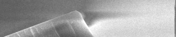

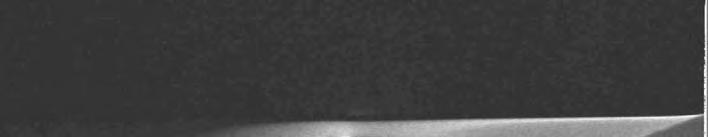


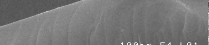
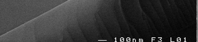
17 SiNW synthesis : Top-down Optmization of the steepness: dry etching parameters (pressure, power) N + Si poly oxide Oxide Accurate control of the Si-poly etching : Nanowire substrate Nanowires with curvature radius ~ 50 nm 17


 N+ Si-poly")


18 SiNW synthesis : Top-down Fabrication of Nanowires resistors Nitride LPCVD Undoped Si- poly Current (A) 2,0x10⁻⁸ 1,5x µm 5 µm 1,0x µm 20 µm 5,0x10⁻⁹ 0,0-1,0-0,5 0,0 0,5 1,0-5,0x10⁻⁹ V oltage (V) N+ Si-poly APCVD oxide -1,0x ,5x ,0x10-8 Current versus voltage for 4lengths of silicon nanowires Thermal oxide Silicon nanowires 18 Si substrate
19 Silicon Nanowire as gas sensor SiNW synthesis : Top-down SiNWs device exposed to smoke SiNWs device exposed to ammonia smoke exposure NH 3 exposure Resista ance ( ) Res sistance ( ) vacuum vacuum vacuum Time (min) Time (min) Ammonia and smoke may act as chemical gates: donor of electrons Carrier transport strongly depends on structural nanowires defects (polysilicon grain boundaries) Gas molecules adsorbed may play a significant role in decreasing the potential barrier height at the grain boundaries between two grains 19


 2,0x10⁻⁸ 1,5x10⁻⁸")


20 SiNW synthesis : Top-down Nanowires Field effect transistors using sidewall spacer process nanowires Vgs = 0V 3,5x10⁻⁸ Vgs = 1V Vgs = 2V 3,0x10⁻⁸ Vgs = 3V Vgs = 4V 2,5x10⁻⁸ S D Ids (A) 2,0x10⁻⁸ 1,5x10⁻⁸ 1,0x10⁻⁸ G N + Substrate 5,0x ,0-5,0x10⁻⁹ 1E Vds (volts) 1E-8 Ids (A) 1E-9 Vds = 4V 1E-10 1E Vgs (volts) 20


21 SiNW synthesis : Top-down To increase the surface APCVD oxide Nanowire Nitride Sacrificial oxide process 21
22 Conclusions and future directions Nanowires synthesis Feasibility of silicon nanowires for both synthesis methods explored Electrical behavior show good potential for electronic devices Curvature radius has to be lowered to observe the nanometric size effects on the electrical behaviour Future directions Detection of chemical and biological species (areas of healthcare, life sciences) Nanowires: new opportunities in this interdisciplinary area diameters comparable to those of the biological/chemical species being sensed. Devices based on nanowires: ultrasensitive electrical sensors for the detection of biological and chemical species. - ability to bind analytes on their surface - direct electrical detection (without using labels) - low concentrations of DNA, proteins or viruses -rapid analysis of these species 22


 Complementary")
23 Conclusions and future directions conductance time Detection of DNA-hybridization P-type FET : the binding of target molecules (negative charges) leads to an accumulation of holes in the nanowire: conductance Probe binding No-complementary targett (no hybridization) Complementary Target (hybridization) 23
24 Conclusions and future directions Detection of proteins Antibody receptor Nanowire modified with specific surface receptors immobilization of antibodies binding of antigens Binding of a protein Biological sensors Specific sensing achieved by linking a recognition group to the surface of the nanowire The nanowire surface can be modified with a variety of linker molecules (bioaffinitive agents): functionalization Significant signal changes with the binding of molecules SiNWs development could significantly impact areas of electronics, genomics, biomedical diagnostics, drug discovery... 24
25 Thank you for your attention 25
Silicon nanowires synthesis for chemical sensor applications
 Silicon nanowires synthesis for chemical sensor applications Fouad Demami, Liang Ni, Regis Rogel, Anne-Claire Salaün, Laurent Pichon To cite this version: Fouad Demami, Liang Ni, Regis Rogel, Anne-Claire
Transistor was first invented by William.B.Shockley, Walter Brattain and John Bardeen of Bell Labratories. In 1961, first IC was introduced.
 Unit 1 Basic MOS Technology Transistor was first invented by William.B.Shockley, Walter Brattain and John Bardeen of Bell Labratories. In 1961, first IC was introduced. Levels of Integration:- i) SSI:-
write-nanocircuits Direct-write Jaebum Joo and Joseph M. Jacobson Molecular Machines, Media Lab Massachusetts Institute of Technology, Cambridge, MA
 Fab-in in-a-box: Direct-write write-nanocircuits Jaebum Joo and Joseph M. Jacobson Massachusetts Institute of Technology, Cambridge, MA April 17, 2008 Avogadro Scale Computing / 1 Avogadro number s? Intel
Major Fabrication Steps in MOS Process Flow
 Major Fabrication Steps in MOS Process Flow UV light Mask oxygen Silicon dioxide photoresist exposed photoresist oxide Silicon substrate Oxidation (Field oxide) Photoresist Coating Mask-Wafer Alignment
CMOS Digital Integrated Circuits Lec 2 Fabrication of MOSFETs
 CMOS Digital Integrated Circuits Lec 2 Fabrication of MOSFETs 1 CMOS Digital Integrated Circuits 3 rd Edition Categories of Materials Materials can be categorized into three main groups regarding their
MEMS in ECE at CMU. Gary K. Fedder
 MEMS in ECE at CMU Gary K. Fedder Department of Electrical and Computer Engineering and The Robotics Institute Carnegie Mellon University Pittsburgh, PA 15213-3890 fedder@ece.cmu.edu http://www.ece.cmu.edu/~mems
Vertical Surround-Gate Field-Effect Transistor
 Chapter 6 Vertical Surround-Gate Field-Effect Transistor The first step towards a technical realization of a nanowire logic element is the design and manufacturing of a nanowire transistor. In this respect,
FABRICATION OF CMOS INTEGRATED CIRCUITS. Dr. Mohammed M. Farag
 FABRICATION OF CMOS INTEGRATED CIRCUITS Dr. Mohammed M. Farag Outline Overview of CMOS Fabrication Processes The CMOS Fabrication Process Flow Design Rules Reference: Uyemura, John P. "Introduction to
EE 5611 Introduction to Microelectronic Technologies Fall Thursday, September 04, 2014 Lecture 02
 EE 5611 Introduction to Microelectronic Technologies Fall 2014 Thursday, September 04, 2014 Lecture 02 1 Lecture Outline Review on semiconductor materials Review on microelectronic devices Example of microelectronic
Semiconductor Physics and Devices
 Metal-Semiconductor and Semiconductor Heterojunctions The Metal-Oxide-Semiconductor Field-Effect Transistor (MOSFET) is one of two major types of transistors. The MOSFET is used in digital circuit, because
按一下以編輯母片標題樣式. Novel Small-Dimension Poly-Si TFTs with Improved Driving Current and Suppressed Short Channel Effects. Hsiao-Wen Zan and Chun-Yen Chang
 Novel Small-Dimension Poly-Si TFTs with Improved Driving Current and Suppressed Short Channel Effects Hsiao-Wen Zan and Chun-Yen Chang Institute of Electronics, National Chiao Tung University, TAIWAN 1
Nanofluidic Diodes based on Nanotube Heterojunctions
 Supporting Information Nanofluidic Diodes based on Nanotube Heterojunctions Ruoxue Yan, Wenjie Liang, Rong Fan, Peidong Yang 1 Department of Chemistry, University of California, Berkeley, CA 94720, USA
Topic 3. CMOS Fabrication Process
 Topic 3 CMOS Fabrication Process Peter Cheung Department of Electrical & Electronic Engineering Imperial College London URL: www.ee.ic.ac.uk/pcheung/ E-mail: p.cheung@ic.ac.uk Lecture 3-1 Layout of a Inverter
IMAGING SILICON NANOWIRES
 Project report IMAGING SILICON NANOWIRES PHY564 Submitted by: 1 Abstract: Silicon nanowires can be easily integrated with conventional electronics. Silicon nanowires can be prepared with single-crystal
Wu Lu Department of Electrical and Computer Engineering and Microelectronics Laboratory, University of Illinois, Urbana, Illinois 61801
 Comparative study of self-aligned and nonself-aligned SiGe p-metal oxide semiconductor modulation-doped field effect transistors with nanometer gate lengths Wu Lu Department of Electrical and Computer
Chapter 3 Fabrication
 Chapter 3 Fabrication The total structure of MO pick-up contains four parts: 1. A sub-micro aperture underneath the SIL The sub-micro aperture is used to limit the final spot size from 300nm to 600nm for
College of Engineering Department of Electrical Engineering and Computer Sciences University of California, Berkeley
 College of Engineering Department of Electrical Engineering and Below are your weekly quizzes. You should print out a copy of the quiz and complete it before your lab section. Bring in the completed quiz
Reconfigurable Si-Nanowire Devices
 Reconfigurable Si-Nanowire Devices André Heinzig, Walter M. Weber, Dominik Martin, Jens Trommer, Markus König and Thomas Mikolajick andre.heinzig@namlab.com log I d Present CMOS technology ~ 88 % of IC
420 Intro to VLSI Design
 Dept of Electrical and Computer Engineering 420 Intro to VLSI Design Lecture 0: Course Introduction and Overview Valencia M. Joyner Spring 2005 Getting Started Syllabus About the Instructor Labs, Problem
Nanostencil Lithography and Nanoelectronic Applications
 Microsystems Laboratory Nanostencil Lithography and Nanoelectronic Applications Oscar Vazquez, Marc van den Boogaart, Dr. Lianne Doeswijk, Prof. Juergen Brugger, LMIS1 Dr. Chan Woo Park, Visiting Professor
End-of-line Standard Substrates For the Characterization of organic
 FRAUNHOFER INSTITUTe FoR Photonic Microsystems IPMS End-of-line Standard Substrates For the Characterization of organic semiconductor Materials Over the last few years, organic electronics have become
Micro-sensors - what happens when you make "classical" devices "small": MEMS devices and integrated bolometric IR detectors
 Micro-sensors - what happens when you make "classical" devices "small": MEMS devices and integrated bolometric IR detectors Dean P. Neikirk 1 MURI bio-ir sensors kick-off 6/16/98 Where are the targets
State-of-the-art device fabrication techniques
 State-of-the-art device fabrication techniques! Standard Photo-lithography and e-beam lithography! Advanced lithography techniques used in semiconductor industry Deposition: Thermal evaporation, e-gun
Lecture 0: Introduction
 Lecture 0: Introduction Introduction Integrated circuits: many transistors on one chip. Very Large Scale Integration (VLSI): bucketloads! Complementary Metal Oxide Semiconductor Fast, cheap, low power
CSCI 2570 Introduction to Nanocomputing
 CSCI 2570 Introduction to Nanocomputing Introduction to NW Decoders John E Savage Lecture Outline Growing nanowires (NWs) Crossbar-based computing Types of NW decoders Resistive model of decoders Addressing
Layout of a Inverter. Topic 3. CMOS Fabrication Process. The CMOS Process - photolithography (2) The CMOS Process - photolithography (1) v o.
 The CMOS Process - photolithography (1) v o.") Layout of a Inverter Topic 3 CMOS Fabrication Process V DD Q p Peter Cheung Department of Electrical & Electronic Engineering Imperial College London v i v o Q n URL: www.ee.ic.ac.uk/pcheung/ E-mail: p.cheung@ic.ac.uk
Layout of a Inverter Topic 3 CMOS Fabrication Process V DD Q p Peter Cheung Department of Electrical & Electronic Engineering Imperial College London v i v o Q n URL: www.ee.ic.ac.uk/pcheung/ E-mail: p.cheung@ic.ac.uk
Investigating the Electronic Behavior of Nano-materials From Charge Transport Properties to System Response
 Investigating the Electronic Behavior of Nano-materials From Charge Transport Properties to System Response Amit Verma Assistant Professor Department of Electrical Engineering & Computer Science Texas
National Centre for Flexible Electronics
 National Centre for Flexible Electronics Tripartite Partnership Government FlexE Centre - A platform for a meaningful interaction between industry and academia. An interdisciplinary team that advances
EE C245 / ME C218 INTRODUCTION TO MEMS DESIGN FALL 2011 PROBLEM SET #2. Due (at 7 p.m.): Tuesday, Sept. 27, 2011, in the EE C245 HW box in 240 Cory.
: Tuesday, Sept. 27, 2011, in the EE C245 HW box in 240 Cory.") Issued: Tuesday, Sept. 13, 2011 PROBLEM SET #2 Due (at 7 p.m.): Tuesday, Sept. 27, 2011, in the EE C245 HW box in 240 Cory. 1. Below in Figure 1.1 is a description of a DRIE silicon etch using the Marvell
Issued: Tuesday, Sept. 13, 2011 PROBLEM SET #2 Due (at 7 p.m.): Tuesday, Sept. 27, 2011, in the EE C245 HW box in 240 Cory. 1. Below in Figure 1.1 is a description of a DRIE silicon etch using the Marvell
ECE 5745 Complex Digital ASIC Design Topic 2: CMOS Devices
 ECE 5745 Complex Digital ASIC Design Topic 2: CMOS Devices Christopher Batten School of Electrical and Computer Engineering Cornell University http://www.csl.cornell.edu/courses/ece5950 Simple Transistor
Low-power carbon nanotube-based integrated circuits that can be transferred to biological surfaces
 SUPPLEMENTARY INFORMATION Articles https://doi.org/10.1038/s41928-018-0056-6 In the format provided by the authors and unedited. Low-power carbon nanotube-based integrated circuits that can be transferred
INTRODUCTION TO MOS TECHNOLOGY
 INTRODUCTION TO MOS TECHNOLOGY 1. The MOS transistor The most basic element in the design of a large scale integrated circuit is the transistor. For the processes we will discuss, the type of transistor
Raman Spectroscopy and Transmission Electron Microscopy of Si x Ge 1-x -Ge-Si Core-Double-Shell Nanowires
 Raman Spectroscopy and Transmission Electron Microscopy of Si x Ge 1-x -Ge-Si Core-Double-Shell Nanowires Paola Perez Mentor: Feng Wen PI: Emanuel Tutuc Background One-dimensional semiconducting nanowires
Session 3: Solid State Devices. Silicon on Insulator
 Session 3: Solid State Devices Silicon on Insulator 1 Outline A B C D E F G H I J 2 Outline Ref: Taurand Ning 3 SOI Technology SOl materials: SIMOX, BESOl, and Smart Cut SIMOX : Synthesis by IMplanted
Supporting Information. Air-stable surface charge transfer doping of MoS 2 by benzyl viologen
 Supporting Information Air-stable surface charge transfer doping of MoS 2 by benzyl viologen Daisuke Kiriya,,ǁ, Mahmut Tosun,,ǁ, Peida Zhao,,ǁ, Jeong Seuk Kang, and Ali Javey,,ǁ,* Electrical Engineering
EE4800 CMOS Digital IC Design & Analysis. Lecture 1 Introduction Zhuo Feng
 EE4800 CMOS Digital IC Design & Analysis Lecture 1 Introduction Zhuo Feng 1.1 Prof. Zhuo Feng Office: EERC 730 Phone: 487-3116 Email: zhuofeng@mtu.edu Class Website http://www.ece.mtu.edu/~zhuofeng/ee4800fall2010.html
LSI ON GLASS SUBSTRATES
 LSI ON GLASS SUBSTRATES OUTLINE Introduction: Why System on Glass? MOSFET Technology Low-Temperature Poly-Si TFT Technology System-on-Glass Technology Issues Conclusion System on Glass CPU SRAM DRAM EEPROM
This Week s Subject. DRAM & Flexible RRAM. p-channel MOSFET (PMOS) CMOS: Complementary Metal Oxide Semiconductor
 CMOS: Complementary Metal Oxide Semiconductor") DRAM & Flexible RRAM This Week s Subject p-channel MOSFET (PMOS) CMOS: Complementary Metal Oxide Semiconductor CMOS Logic Inverter NAND gate NOR gate CMOS Integration & Layout GaAs MESFET (JFET) 1 Flexible
DRAM & Flexible RRAM This Week s Subject p-channel MOSFET (PMOS) CMOS: Complementary Metal Oxide Semiconductor CMOS Logic Inverter NAND gate NOR gate CMOS Integration & Layout GaAs MESFET (JFET) 1 Flexible
+1 (479)
") Introduction to VLSI Design http://csce.uark.edu +1 (479) 575-6043 yrpeng@uark.edu Invention of the Transistor Vacuum tubes ruled in first half of 20th century Large, expensive, power-hungry, unreliable
Introduction to VLSI Design http://csce.uark.edu +1 (479) 575-6043 yrpeng@uark.edu Invention of the Transistor Vacuum tubes ruled in first half of 20th century Large, expensive, power-hungry, unreliable
INTRODUCTION: Basic operating principle of a MOSFET:
 INTRODUCTION: Along with the Junction Field Effect Transistor (JFET), there is another type of Field Effect Transistor available whose Gate input is electrically insulated from the main current carrying
Supplementary Materials for
 www.sciencemag.org/cgi/content/full/science.1234855/dc1 Supplementary Materials for Taxel-Addressable Matrix of Vertical-Nanowire Piezotronic Transistors for Active/Adaptive Tactile Imaging Wenzhuo Wu,
High-yield Fabrication Methods for MEMS Tilt Mirror Array for Optical Switches
 : MEMS Device Technologies High-yield Fabrication Methods for MEMS Tilt Mirror Array for Optical Switches Joji Yamaguchi, Tomomi Sakata, Nobuhiro Shimoyama, Hiromu Ishii, Fusao Shimokawa, and Tsuyoshi
Section 2: Lithography. Jaeger Chapter 2 Litho Reader. The lithographic process
 Section 2: Lithography Jaeger Chapter 2 Litho Reader The lithographic process Photolithographic Process (a) (b) (c) (d) (e) (f) (g) Substrate covered with silicon dioxide barrier layer Positive photoresist
Section 2: Lithography. Jaeger Chapter 2 Litho Reader. EE143 Ali Javey Slide 5-1
 Section 2: Lithography Jaeger Chapter 2 Litho Reader EE143 Ali Javey Slide 5-1 The lithographic process EE143 Ali Javey Slide 5-2 Photolithographic Process (a) (b) (c) (d) (e) (f) (g) Substrate covered
Organic Electronics. Information: Information: 0331a/ 0442/
 Organic Electronics (Course Number 300442 ) Spring 2006 Organic Field Effect Transistors Instructor: Dr. Dietmar Knipp Information: Information: http://www.faculty.iubremen.de/course/c30 http://www.faculty.iubremen.de/course/c30
2.8 - CMOS TECHNOLOGY
 CMOS Technology (6/7/00) Page 1 2.8 - CMOS TECHNOLOGY INTRODUCTION Objective The objective of this presentation is: 1.) Illustrate the fabrication sequence for a typical MOS transistor 2.) Show the physical
CMP for More Than Moore
 2009 Levitronix Conference on CMP Gerfried Zwicker Fraunhofer Institute for Silicon Technology ISIT Itzehoe, Germany gerfried.zwicker@isit.fraunhofer.de Contents Moore s Law and More Than Moore Comparison:
Supplementary Figures
 Supplementary Figures Supplementary Figure 1 The diameter and length of AgNWs. (a) SEM image and (b) AFM image of AgNWs coated on a SiO2/Si wafer at 500 rpm for 30 sec. The diameter and length of the AgNWs
Electronic sensor for ph measurements in nanoliters
 Electronic sensor for ph measurements in nanoliters Ismaïl Bouhadda, Olivier De Sagazan, France Le Bihan To cite this version: Ismaïl Bouhadda, Olivier De Sagazan, France Le Bihan. Electronic sensor for
SUPPLEMENTARY INFORMATION
 SUPPLEMENTARY INFORMATION doi:10.1038/nature11293 1. Formation of (111)B polar surface on Si(111) for selective-area growth of InGaAs nanowires on Si. Conventional III-V nanowires (NWs) tend to grow in
3D SOI elements for System-on-Chip applications
 Advanced Materials Research Online: 2011-07-04 ISSN: 1662-8985, Vol. 276, pp 137-144 doi:10.4028/www.scientific.net/amr.276.137 2011 Trans Tech Publications, Switzerland 3D SOI elements for System-on-Chip
The Department of Advanced Materials Engineering. Materials and Processes in Polymeric Microelectronics
 The Department of Advanced Materials Engineering Materials and Processes in Polymeric Microelectronics 1 Outline Materials and Processes in Polymeric Microelectronics Polymeric Microelectronics Process
High-Ohmic Resistors using Nanometer-Thin Pure-Boron Chemical-Vapour-Deposited Layers
 High-Ohmic Resistors using Nanometer-Thin Pure-Boron Chemical-Vapour-Deposited Layers Negin Golshani, Vahid Mohammadi, Siva Ramesh, Lis K. Nanver Delft University of Technology The Netherlands ESSDERC
SYNTHESIS AND ANALYSIS OF SILICON NANOWIRES GROWN ON Si (111) SUBSTRATE AT DIFFERENT SILANE GAS FLOW RATE
 SUBSTRATE AT DIFFERENT SILANE GAS FLOW RATE") SYNTHESIS AND ANALYSIS OF SILICON NANOWIRES GROWN ON Si (111) SUBSTRATE AT DIFFERENT SILANE GAS FLOW RATE Habib Hamidinezhad*, Yussof Wahab, Zulkafli Othaman and Imam Sumpono Ibnu Sina Institute for Fundamental
SYNTHESIS AND ANALYSIS OF SILICON NANOWIRES GROWN ON Si (111) SUBSTRATE AT DIFFERENT SILANE GAS FLOW RATE Habib Hamidinezhad*, Yussof Wahab, Zulkafli Othaman and Imam Sumpono Ibnu Sina Institute for Fundamental
MOSFET & IC Basics - GATE Problems (Part - I)
") MOSFET & IC Basics - GATE Problems (Part - I) 1. Channel current is reduced on application of a more positive voltage to the GATE of the depletion mode n channel MOSFET. (True/False) [GATE 1994: 1 Mark]
MOSFET & IC Basics - GATE Problems (Part - I) 1. Channel current is reduced on application of a more positive voltage to the GATE of the depletion mode n channel MOSFET. (True/False) [GATE 1994: 1 Mark]
VLSI Design. Introduction
 VLSI Design Introduction Outline Introduction Silicon, pn-junctions and transistors A Brief History Operation of MOS Transistors CMOS circuits Fabrication steps for CMOS circuits Introduction Integrated
Chapter 15 Summary and Future Trends
 Chapter 15 Summary and Future Trends Hong Xiao, Ph. D. hxiao89@hotmail.com www2.austin.cc.tx.us/hongxiao/book.htm Hong Xiao, Ph. D. www2.austin.cc.tx.us/hongxiao/book.htm 1 The 1960s First IC product Bipolar
Supplementary Information
 Supplementary Information Wireless thin film transistor based on micro magnetic induction coupling antenna Byoung Ok Jun 1, Gwang Jun Lee 1, Jong Gu Kang 1,2, Seung Uk Kim 1, Ji Woong Choi 1, Seung Nam
Coating of Si Nanowire Array by Flexible Polymer
 , pp.422-426 http://dx.doi.org/10.14257/astl.2016.139.84 Coating of Si Nanowire Array by Flexible Polymer Hee- Jo An 1, Seung-jin Lee 2, Taek-soo Ji 3* 1,2.3 Department of Electronics and Computer Engineering,
Nanotechnology, the infrastructure, and IBM s research projects
 Nanotechnology, the infrastructure, and IBM s research projects Dr. Paul Seidler Coordinator Nanotechnology Center, IBM Research - Zurich Nanotechnology is the understanding and control of matter at dimensions
The Design and Realization of Basic nmos Digital Devices
 Proceedings of The National Conference On Undergraduate Research (NCUR) 2004 Indiana University Purdue University Indianapolis, Indiana April 15-17, 2004 The Design and Realization of Basic nmos Digital
Lecture: Integration of silicon photonics with electronics. Prepared by Jean-Marc FEDELI CEA-LETI
 Lecture: Integration of silicon photonics with electronics Prepared by Jean-Marc FEDELI CEA-LETI Context The goal is to give optical functionalities to electronics integrated circuit (EIC) The objectives
VLSI Design. Introduction
 Tassadaq Hussain VLSI Design Introduction Outcome of this course Problem Aims Objectives Outcomes Data Collection Theoretical Model Mathematical Model Validate Development Analysis and Observation Pseudo
Sensitive Continuous Monitoring of ph thanks to Matrix of several Suspended Gate Field Effect Transistors. Introduction
 Sensitive Continuous Monitoring of thanks to Matrix of several Suspended Gate Field Effect Transistors B. da Silva Rodrigues a,b, O. De Sagazan a, S. Crand a, F. LeBihan a, O. Bonnaud a, T. Mohammed-Brahim
Transparent p-type SnO Nanowires with Unprecedented Hole Mobility among Oxide Semiconductors
 Supplementary Information Transparent p-type SnO Nanowires with Unprecedented Hole Mobility among Oxide Semiconductors J. A. Caraveo-Frescas and H. N. Alshareef* Materials Science and Engineering, King
Alternatives to standard MOSFETs. What problems are we really trying to solve?
 Alternatives to standard MOSFETs A number of alternative FET schemes have been proposed, with an eye toward scaling up to the 10 nm node. Modifications to the standard MOSFET include: Silicon-in-insulator
Characterization of SOI MOSFETs by means of charge-pumping
 Paper Characterization of SOI MOSFETs by means of charge-pumping Grzegorz Głuszko, Sławomir Szostak, Heinrich Gottlob, Max Lemme, and Lidia Łukasiak Abstract This paper presents the results of charge-pumping
Atomic-layer deposition of ultrathin gate dielectrics and Si new functional devices
 Atomic-layer deposition of ultrathin gate dielectrics and Si new functional devices Anri Nakajima Research Center for Nanodevices and Systems, Hiroshima University 1-4-2 Kagamiyama, Higashi-Hiroshima,
A COMPARITIVE ANALYSIS ON NANOWIRE BASED MEMS PRESSURE SENSOR
 A COMPARITIVE ANALYSIS ON NANOWIRE BASED MEMS PRESSURE SENSOR Abstract S.Maflin Shaby Electronic and Telecommunication Enginering, Sathyabam University, Jeppiaar Nager, Chennai600119,India. maflinshaby@yahoo.co.in.
SAMPLE SLIDES & COURSE OUTLINE. Core Competency In Semiconductor Technology: 2. FABRICATION. Dr. Theodore (Ted) Dellin
 Dellin") & Digging Deeper Devices, Fabrication & Reliability For More Info:.com or email Dellin@ieee.org SAMPLE SLIDES & COURSE OUTLINE In : 2. A Easy, Effective, of How Devices Are.. Recommended for everyone who
& Digging Deeper Devices, Fabrication & Reliability For More Info:.com or email Dellin@ieee.org SAMPLE SLIDES & COURSE OUTLINE In : 2. A Easy, Effective, of How Devices Are.. Recommended for everyone who
High throughput ultra-long (20cm) nanowire fabrication using a. wafer-scale nanograting template
 nanowire fabrication using a. wafer-scale nanograting template") Supporting Information High throughput ultra-long (20cm) nanowire fabrication using a wafer-scale nanograting template Jeongho Yeon 1, Young Jae Lee 2, Dong Eun Yoo 3, Kyoung Jong Yoo 2, Jin Su Kim 2,
Supporting Information High throughput ultra-long (20cm) nanowire fabrication using a wafer-scale nanograting template Jeongho Yeon 1, Young Jae Lee 2, Dong Eun Yoo 3, Kyoung Jong Yoo 2, Jin Su Kim 2,
Hermetic Packaging Solutions using Borosilicate Glass Thin Films. Lithoglas Hermetic Packaging Solutions using Borosilicate Glass Thin Films
 Hermetic Packaging Solutions using Borosilicate Glass Thin Films 1 Company Profile Company founded in 2006 ISO 9001:2008 qualified since 2011 Headquarters and Production in Dresden, Germany Production
Notes. (Subject Code: 7EC5)
") COMPUCOM INSTITUTE OF TECHNOLOGY & MANAGEMENT, JAIPUR (DEPARTMENT OF ELECTRONICS & COMMUNICATION) Notes VLSI DESIGN NOTES (Subject Code: 7EC5) Prepared By: MANVENDRA SINGH Class: B. Tech. IV Year, VII
COMPUCOM INSTITUTE OF TECHNOLOGY & MANAGEMENT, JAIPUR (DEPARTMENT OF ELECTRONICS & COMMUNICATION) Notes VLSI DESIGN NOTES (Subject Code: 7EC5) Prepared By: MANVENDRA SINGH Class: B. Tech. IV Year, VII
Parallel Alignment of Nanowires for Fast Fabrication of Nanowire Based Gas Sensors
 Parallel Alignment of Nanowires for Fast Fabrication of Nanowire Based Gas Sensors R. Jiménez-Díaz 1, J.D. Prades 1 F. Hernández-Ramírez, J. Santander 3 C. Calaza 3, L. Fonseca 3, C. Cané 3 A. Romano-Rodriguez
Measurement of Microscopic Three-dimensional Profiles with High Accuracy and Simple Operation
 238 Hitachi Review Vol. 65 (2016), No. 7 Featured Articles Measurement of Microscopic Three-dimensional Profiles with High Accuracy and Simple Operation AFM5500M Scanning Probe Microscope Satoshi Hasumura
Photolithography I ( Part 1 )
") 1 Photolithography I ( Part 1 ) Chapter 13 : Semiconductor Manufacturing Technology by M. Quirk & J. Serda Bjørn-Ove Fimland, Department of Electronics and Telecommunication, Norwegian University of Science
1 Photolithography I ( Part 1 ) Chapter 13 : Semiconductor Manufacturing Technology by M. Quirk & J. Serda Bjørn-Ove Fimland, Department of Electronics and Telecommunication, Norwegian University of Science
Section 2: Lithography. Jaeger Chapter 2. EE143 Ali Javey Slide 5-1
 Section 2: Lithography Jaeger Chapter 2 EE143 Ali Javey Slide 5-1 The lithographic process EE143 Ali Javey Slide 5-2 Photolithographic Process (a) (b) (c) (d) (e) (f) (g) Substrate covered with silicon
Design Simulation and Analysis of NMOS Characteristics for Varying Oxide Thickness
 MIT International Journal of Electronics and Communication Engineering, Vol. 4, No. 2, August 2014, pp. 81 85 81 Design Simulation and Analysis of NMOS Characteristics for Varying Oxide Thickness Alpana
High-Speed Scalable Silicon-MoS 2 P-N Heterojunction Photodetectors
 High-Speed Scalable Silicon-MoS 2 P-N Heterojunction Photodetectors Veerendra Dhyani 1, and Samaresh Das 1* 1 Centre for Applied Research in Electronics, Indian Institute of Technology Delhi, New Delhi-110016,
Deliverable 4.2: TEM cross sections on prototyped Gated Resistors
 Deliverable 4.2: TEM cross sections on prototyped Gated Resistors Olga G. Varona, Geoff Walsh, Bernie Capraro Intel Ireland 21 June 2011 Abbreviation list D: drain FIB: focused ion-beam HRTEM: high resolution
Electrothermal Actuator
 Electrothermal Actuator 09-09-14 Generated by CleanRoom Substrate thickness: 50 (µm) Comments: 1. Substrate Si Czochralski (100) Film Thickness: 600 nm (Conformal) Comments: 2. Deposition Si3N4 PECVD (Ar)
4.1.2 InAs nanowire circuits fabricated by field-assisted selfassembly on a host substrate
 22 Annual Report 2010 - Solid-State Electronics Department 4.1.2 InAs nanowire circuits fabricated by field-assisted selfassembly on a host substrate Student Scientist in collaboration with R. Richter
Class Website: p b2008.htm
 EEE598 Molecular Electronics Some Information about the Course Instructor: Dr. Nongjian Tao (njtao@asu.edu) Where: ECA 219 When: TTH 12:00 1:15 pm Office Hours: TTH 1:30-2:30 p.m. or by appointment. Office
Pattern Transfer CD-AFM. Resist Features on Poly. Poly Features on Oxide. Quate Group, Stanford University
 Resist Features on Poly Pattern Transfer Poly Features on Oxide CD-AFM The Critical Dimension AFM Boot -Shaped Tip Tip shape is optimized to sense topography on vertical surfaces Two-dimensional feedback
64 Channel Flip-Chip Mounted Selectively Oxidized GaAs VCSEL Array
 64 Channel Flip-Chip Mounted Selectively Oxidized GaAs VCSEL Array 69 64 Channel Flip-Chip Mounted Selectively Oxidized GaAs VCSEL Array Roland Jäger and Christian Jung We have designed and fabricated
Gigahertz Ambipolar Frequency Multiplier Based on Cvd Graphene
 Gigahertz Ambipolar Frequency Multiplier Based on Cvd Graphene The MIT Faculty has made this article openly available. Please share how this access benefits you. Your story matters. Citation As Published
Wafer-level Vacuum Packaged X and Y axis Gyroscope Using the Extended SBM Process for Ubiquitous Robot applications
 Proceedings of the 17th World Congress The International Federation of Automatic Control Wafer-level Vacuum Packaged X and Y axis Gyroscope Using the Extended SBM Process for Ubiquitous Robot applications
High-Performance Si Nanowire FET with a Semi Gate-Around Structure Suitable for Integration
 High-Performance Si Nanowire FET with a Semi Gate-Around Structure Suitable for Integration Soshi Sato 1, Hideyuki Kamimura 1, Hideaki Arai 1, Kuniyuki Kakushima 2, Parhat Ahmet 1, Kenji Ohmori 3, Keisaku
A large-area wireless power transmission sheet using printed organic. transistors and plastic MEMS switches
 Supplementary Information A large-area wireless power transmission sheet using printed organic transistors and plastic MEMS switches Tsuyoshi Sekitani 1, Makoto Takamiya 2, Yoshiaki Noguchi 1, Shintaro
4.1 Device Structure and Physical Operation
 10/12/2004 4_1 Device Structure and Physical Operation blank.doc 1/2 4.1 Device Structure and Physical Operation Reading Assignment: pp. 235-248 Chapter 4 covers Field Effect Transistors ( ) Specifically,
Chapter 3: Basics Semiconductor Devices and Processing 2006/9/27 1. Topics
 Chapter 3: Basics Semiconductor Devices and Processing 2006/9/27 1 Topics What is semiconductor Basic semiconductor devices Basics of IC processing CMOS technologies 2006/9/27 2 1 What is Semiconductor
Key Questions. ECE 340 Lecture 39 : Introduction to the BJT-II 4/28/14. Class Outline: Fabrication of BJTs BJT Operation
 Things you should know when you leave ECE 340 Lecture 39 : Introduction to the BJT-II Fabrication of BJTs Class Outline: Key Questions What elements make up the base current? What do the carrier distributions
Monolithically integrated InGaAs nanowires on 3D. structured silicon-on-insulator as a new platform for. full optical links
 Monolithically integrated InGaAs nanowires on 3D structured silicon-on-insulator as a new platform for full optical links Hyunseok Kim 1, Alan C. Farrell 1, Pradeep Senanayake 1, Wook-Jae Lee 1,* & Diana.
Chapter 3 Basics Semiconductor Devices and Processing
 Chapter 3 Basics Semiconductor Devices and Processing 1 Objectives Identify at least two semiconductor materials from the periodic table of elements List n-type and p-type dopants Describe a diode and
EE143 Fall 2016 Microfabrication Technologies. Lecture 3: Lithography Reading: Jaeger, Chap. 2
 EE143 Fall 2016 Microfabrication Technologies Lecture 3: Lithography Reading: Jaeger, Chap. 2 Prof. Ming C. Wu wu@eecs.berkeley.edu 511 Sutardja Dai Hall (SDH) 1-1 The lithographic process 1-2 1 Photolithographic
ADVANCED MATERIALS AND PROCESSES FOR NANOMETER-SCALE FINFETS
 ADVANCED MATERIALS AND PROCESSES FOR NANOMETER-SCALE FINFETS Tsu-Jae King, Yang-Kyu Choi, Pushkar Ranade^ and Leland Chang Electrical Engineering and Computer Sciences Dept., ^Materials Science and Engineering
Contents. Nano-2. Nano-2. Nanoscience II: Nanowires. 2. Growth of nanowires. 1. Nanowire concepts Nano-2. Nano-2
 Contents Nanoscience II: Nanowires Kai Nordlund 17.11.2010 Faculty of Science Department of Physics Division of Materials Physics 1. Introduction: nanowire concepts 2. Growth of nanowires 1. Spontaneous
In this lecture we will begin a new topic namely the Metal-Oxide-Semiconductor Field Effect Transistor.
 Solid State Devices Dr. S. Karmalkar Department of Electronics and Communication Engineering Indian Institute of Technology, Madras Lecture - 38 MOS Field Effect Transistor In this lecture we will begin
New Pixel Circuits for Driving Organic Light Emitting Diodes Using Low-Temperature Polycrystalline Silicon Thin Film Transistors
 Chapter 4 New Pixel Circuits for Driving Organic Light Emitting Diodes Using Low-Temperature Polycrystalline Silicon Thin Film Transistors ---------------------------------------------------------------------------------------------------------------
Highly efficient SERS nanowire/ag composites
 Highly efficient SERS nanowire/ag composites S.M. Prokes, O.J. Glembocki and R.W. Rendell Electronics Science and Technology Division Introduction: Optically based sensing provides advantages over electronic