Nano-structured superconducting single-photon detector
|
|
|
- Winfred Hampton
- 6 years ago
- Views:
Transcription
1 Nano-structured superconducting single-photon detector G. Gol'tsman *a, A. Korneev a,v. Izbenko a, K. Smirnov a, P. Kouminov a, B. Voronov a, A. Verevkin b, J. Zhang b, A. Pearlman b, W. Slysz b, and R. Sobolewski b a Moscow State Pedagogical University, Malaya Pirogovskaya 1, Moscow, 11992, Russia b University of Rochester, NY , USA Outline 1. Motivation for development of IR Single-Photon Detector 2. Fabrication and design of NbN SPD 3.Mechanism of SSPD photon detection 4.Time constant and jitter of NbN SPD 5.Quantum efficiency and spectral sensitivity 6.Dark counts rate and noise equivalent power 7. Implementation of NbN SPD: Silicon IC Debug 8. Conclusions
2 Vdd (1) Motivation: CMOS Device Debug Normally operating nmos transistor emits near IR photons ( um) when current passes through the channel Time-correlated photon emission detection measures transistor switching time Vdd (1) Vdd (1) Vss (0) Vss (0) Vss (0) Kash, J. A. and J. C.-H. Tsang (1999). Noninvasive optical method for measuring internal switching and other dynamic parameters of CMOS circuits. USA, International Business Machines Corporation. US Patent # 5,940,545
3 Specifications for some commercially available single-photon detectors and NbN SSPD at 1.3 micron wavelength Detector Model Counting rate (s -1 ) DE (%) Jitter (ps) * Gated regime with 0.1% per gate after-count probability. ** Calculated with 10-4 per gate probability. *** Data for a high-speed version; standard devices exhibit s -1. Dark counts (s -1 ) FPD5W1KS InGaAs APD 5.0x ** (Fujitsu) R STOP PMT 9.0x x10 4 (Hamamatsu) Si APD SPCM -AQR x (EG&G) Mersicron II PMT 1.0x10 6*** (Quantar Tech.Inc) Superconducting Tunnel 5.0x N/A N/A Junction SSPD (measured) 3x <10-4
4 Emission from Good and Bad Transistors (Mepsicron II detector) 0.35um, 3.3V CMOS device running at 100MHz Good Leaky Counts Time (ns)

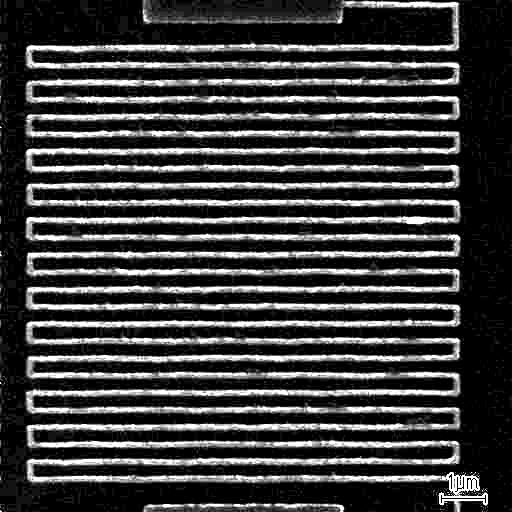
5 Structure: NbN Meander Line Pattern SSPD Meander Line Fabrication Meander used to increase detector active area 15um x 15um AFM image of NbN structure Fabrication: Sputter nm thick NbN film on sapphire substrate. Form Au contacts with Optical lithography. Form 150nm wide meander line pattern with e-beam lithography. Requirements: Uniform film material and thickness. Uniform line width. High substrate surface quality.
6 SSPD Requirements N SSPD Requirement Our option 1 Superconducting NbN material 2 thin and narrow Thickness of NbN film strips 3.5 nm 3 Covered area and filling factor Width of strip ~100 nm Meander type device with 4 4 or µm 2 area Filling factor up to 0.5
7 SSPD Requirements L D filling factor: D/L
8 Fabrication of SSPD Using Direct Electron Beam Lithography and Reactive Ion Etching Process ID# Sketch Comments 1. Deposition of a NbN film by dc reactive magnetron sputtering. Substrate Substrate: double-side-polished, 300-µm-thick sapphire. Residual pressure mbar. Substrate temperature C. N 2 partial pressure 10-4 mbar. Ar partial pressure mbar. 2. Patterning of alignment marks. Lift-off process. Ti/Au 5/100 nm alignment marks. Vacuum resistive evaporation at room temperature. Optical lithography process with AZ1512 photoresist. 3. Patterning of stripe windows in preparation for a meander structure. Direct electron beam lithography process with PMMA 950K (2%, 0.08 µm) electron resist. Process parameters: I = 25 pa, U = 25kV. The developer: toluene and isopropanol 1:10 mixture. Reactive ion etching of NbN film in SF 6. Removal of electron resist layer.
9 Fabrication of SSPD Using Direct Electron Beam Lithography and Reactive Ion Etching Process ID# Sketch Comments 4. Patterning of outer contact pads. Lift-off process. Ti/Au 5/200 nm contact pads. Vacuum resistive evaporation at room temperature. Optical lithography process with AZ1512 photoresist. 5. Final patterning of meander structure. Photolithography process with AZ1512 photoresist. Chemical etching of unprotected areas of NbN film in CP 4 (HNO 3 /HF/CH 3 COOH (5:3:3)). Removal of electron resist layer.
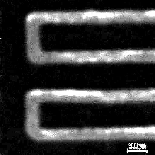
 Scanning Electron microscope image filling factor")
10 Images of SSPD (direct electron beam lithography and reactive ion etching process) Scanning Electron microscope image filling factor 1/2

11 Scanning Electron microscope image.
12 Resistance vs Temperature Curves for Sputtered NbN Film 3.5 nm Thick and for SSPD Device Direct electron beam lithography and reactive ion etching process
13 Energy Relaxation Process 10 0 Photon hν e-e interaction 10-1 ev e-e interaction Debye phonons k b T Cooper pairs Quasi particles Schematic description of relaxation process in an optically excited superconducting thin film.


14 Mechanism of SSPD Photon Detection
15 IV-curves of the 3.5-nm thick film devices at 4.5 K Superconducting state current, µa I c A 50 Ω load line Resistive state B 5 Metastable Region Voltage, mv
16 Response of NbN SPD with 3.5 nm film thickness single-photon response ps Voltage, V Time, ps
17 Experimental setup with variable optical delay
18 Pulse patterns at different optical delays. (a) delay = 0; (b) delay = 100ps, we can see the signature of the delayed pulse; (c) delay = 330ps; (d) delay = 650ps; (e) delay = 1080ps.
19 SPD s Spectral Sensitivity 100 detection efficiency,% wavelength, µm Detection efficiency vs radiation wavelength for the devices made from 3.5 nm-thick NbN films.
20 Quantum efficiency and dark counts rate vs bias current. QE, % QE at wavelength 1.55 µm 1.26 µm 0.94 µm 0.67 µm 0.56 µm I/Ic Dark counts measured extrapolated Dark counts per second
21 NEP as a function of the bias current in the visible and IR ranges. NEP (W/Hz 1/2 ) Measured: 1.55 µm 1.26 µm 0.94 µm 0.67 µm 0.56 µm Extrapolated: 1.55 µm 1.26 µm 0.94 µm 0.67 µm 0.56 µm Noise Equivalent Power (NEP) hv NEP = 2R DE I/I c
22 Time-Resolved Photon Emission (TRPE) System Setup with Internal-Optical Fiber Alignment NPTest company
23 Closed-cycle Cryostat NPTest company
24 Application: Silicon IC Debug Photon emission correlated with transistor switching event Test chip: 0.13 um, 1.3V CMOS device running at 100 MHz NPTest company Emission detected by SPD ( Speedy ) from nmos transistor

25 Precise Timing Analysis with SPD Pulse position measures transistor switching timing < 10 ps edge timing accuracy Pulse width related to transistor switching time NPTest company
26 Single-photon emission from a CMOS VLSI chip Photon counting histogram from a 0.13 µm, 1.3 V CMOS chip running at 100 MHz measured with 3.5-nm-thick NbN SSPD with bias current of 0.85 I c. NPTest company
27 The relationship of T acq versus 1/(kQE) for TRPE system T acq = T loop ttts 2 kqe + ttts R ( ) 2 t ( kqe) dk, T loop is the loop length of the test ttts t R dk k is the jitter of the detector system is the timing accuracy required is the dark counting rate is a factor dependent on the strength of photon emission from the transistor and the photon collection efficiency of the optical system NPTest company
28 Conclusions NbN SSPDs are sensitive to radiation from UV to mid-ir. 3.5-nm-thick devices approach detection efficiency DE = 10 % at ~ µm, related to intrinsic QE close to 100 %. Voltage pulse has FWHM and risetime of about 150 ps and 100 ps, respectively, limited by read-out electronics; experimentally measured repetition rate in single-photon regime is 3 GHz. Jitter is about 20 ps ; significantly lower comparing with any semiconductor detectors. Dark counting rate is extremely low 10-4 counts per second and less. Dynamic range is about 130 db. Measured NEP is about W/Hz 1/2 at 1.3 micron wavelength and less than W/Hz 1/2 in the visible range. NbN SSPD is practical device for non-invasive optical analysis of Si CMOS circuits.
Spectral Sensitivity and Temporal Resolution of NbN Superconducting Single-Photon Detectors
 Spectral Sensitivity and Temporal Resolution of NbN Superconducting Single-Photon Detectors A. Verevkin, J. Zhang l, W. Slysz-, and Roman Sobolewski3 Department of Electrical and Computer Engineering and
Ultrafast Superconducting Single-Photon Optical Detectors and Their Applications
 Ultrafast Superconducting Single-Photon Optical Detectors and Their Applications Introduction Single-photon detectors (SPD s) represent the ultimate sensitivity limit for any quantum radiation detectors.
NbN nanowire superconducting single-photon detector for mid-infrared
 Available online at www.sciencedirect.com Physics Procedia 36 (2012 ) 72 76 Superconductivity Centennial Conference NbN nanowire superconducting single-photon detector for mid-infrared A. Korneev, Yu.
Superconducting single-photon detectors as photon-energy and polarization resolving devices. Roman Sobolewski
 Superconducting single-photon detectors as photon-energy and polarization resolving devices Roman Sobolewski Departments of Electrical and Computing Engineering Physics and Astronomy, Materials Science
Superconducting Nanowire Single Photon Detector (SNSPD) integrated with optical circuits
 integrated with optical circuits") Superconducting Nanowire Single Photon Detector (SNSPD) integrated with optical circuits Marcello Graziosi, ESR 3 within PICQUE (Marie Curie ITN project) and PhD student marcello.graziosi@ifn.cnr.it Istituto
Superconducting Nanowire Single Photon Detector (SNSPD) integrated with optical circuits Marcello Graziosi, ESR 3 within PICQUE (Marie Curie ITN project) and PhD student marcello.graziosi@ifn.cnr.it Istituto
Waveguide superconducting single-photon detectors for Integrated Quantum Photonic devices
 Waveguide superconducting single-photon detectors for Integrated Quantum Photonic devices KOBIT- 1 Izmir Yuksek Teknoloji Enstitusu Döndü Sahin QET Labs, d.sahin@bristol.ac.uk EU-FP7 Implementing QNIX
Spectral Sensitivity of the NbN Single-Photon Superconducting Detector
 IEICE TRANS. ELECTRON., VOL.E85 C, NO.3 MARCH 2002 797 INVITED PAPER Special Issue on Superconductive Electronics Spectral Sensitivity of the NbN Single-Photon Superconducting Detector Roman SOBOLEWSKI,
photolithographic techniques (1). Molybdenum electrodes (50 nm thick) are deposited by
. Molybdenum electrodes (50 nm thick) are deposited by") Supporting online material Materials and Methods Single-walled carbon nanotube (SWNT) devices are fabricated using standard photolithographic techniques (1). Molybdenum electrodes (50 nm thick) are deposited
Supporting online material Materials and Methods Single-walled carbon nanotube (SWNT) devices are fabricated using standard photolithographic techniques (1). Molybdenum electrodes (50 nm thick) are deposited
Single-photon source characterization with infrared-sensitive superconducting single-photon detectors
 1 Single-photon source characterization with infrared-sensitive superconducting single-photon detectors Robert H. Hadfield a), Martin J. Stevens, Richard P. Mirin, Sae Woo Nam National Institute of Standards
Noise temperature measurements of NbN phonon-cooled Hot Electron Bolometer mixer at 2.5 and 3.8 THz.
 Noise temperature measurements of NbN phonon-cooled Hot Electron Bolometer mixer at 2.5 and 3.8 THz. ABSTRACT Yu. B. Vachtomin, S. V. Antipov, S. N. Maslennikov, K. V. Smirnov, S. L. Polyakov, N. S. Kaurova,
Christian Boit TUB Berlin University of Technology Sect. Semiconductor Devices. 1
 Semiconductor Device & Analysis Center Berlin University of Technology Christian Boit TUB Berlin University of Technology Sect. Semiconductor Devices Christian.Boit@TU-Berlin.DE 1 Semiconductor Device
YBa 2 Cu 3 O 7-δ Hot-Electron Bolometer Mixer at 0.6 THz
 YBa 2 Cu 3 O 7-δ Hot-Electron Bolometer Mixer at 0.6 THz S.Cherednichenko 1, F.Rönnung 2, G.Gol tsman 3, E.Kollberg 1 and D.Winkler 2 1 Department of Microelectronics, Chalmers University of Technology,
Supporting Information. Vertical Graphene-Base Hot-Electron Transistor
 Supporting Information Vertical Graphene-Base Hot-Electron Transistor Caifu Zeng, Emil B. Song, Minsheng Wang, Sejoon Lee, Carlos M. Torres Jr., Jianshi Tang, Bruce H. Weiller, and Kang L. Wang Department
Noise and Gain Performance of spiral antenna coupled HEB Mixers at 0.7 THz and 2.5 THz.
 14th International Symposium on Space Terahertz Technology Noise and Gain Performance of spiral antenna coupled HEB Mixers at 0.7 THz and 2.5 THz. K.V. Smimov, Yu.B. Vachtomin, S.V. Antipo-v, S.N. IVIaslennikov,
Low noise THz NbN HEB mixers for radio astronomy: Development at Chalmers/ MC2
 Low noise THz NbN HEB mixers for radio astronomy: Development at Chalmers/ MC2 Sergey Cherednichenko Department of Microtechnology and Nanoscience, MC2 Chalmers University of Technology, SE-412 96, Gothenburg,
Supplementary information
 Supplementary information Supplementary figures Supplementary Figure S1. Characterization of the superconducting films. a) Atomic force microscope (AFM) measurements of the NbN film morphology after deposition
P-CUBE-Series High Sensitivity PIN Detector Modules
 High Sensitivity PIN Detector Modules Description The P-CUBE-series manufactured by LASER COMPONENTS has been designed for customers interested in experimenting with low noise silicon or InGaAs pin detectors.
Silicon Carbide Solid-State Photomultiplier for UV Light Detection
 Silicon Carbide Solid-State Photomultiplier for UV Light Detection Sergei Dolinsky, Stanislav Soloviev, Peter Sandvik, and Sabarni Palit GE Global Research 1 Why Solid-State? PMTs are sensitive to magnetic
Redefining Measurement ID101 OEM Visible Photon Counter
 Redefining Measurement ID OEM Visible Photon Counter Miniature Photon Counter for OEM Applications Intended for large-volume OEM applications, the ID is the smallest, most reliable and most efficient single-photon
A single-photon detector with high efficiency. and sub-10 ps time resolution
 A single-photon detector with high efficiency and sub-10 ps time resolution arxiv:1801.06574v1 [physics.ins-det] 19 Jan 2018 Iman Esmaeil Zadeh,,, Johannes W. N. Los, Ronan B. M. Gourgues, Gabriele Bulgarini,
Resolving Dark Pulses from Photon Pulses in NbN Superconducting Single-Photon Detectors
 Resolving Dark Pulses from Photon Pulses in NbN Superconducting Single-Photon Detectors Introduction Fast and reliable single-photon detectors (SPD s) have become a highly sought after technology in recent
2007 IEEE. Personal use of this material is permitted. However, permission to reprint/republish this material for advertising or promotional purposes
 2007 IEEE. Personal use of this material is permitted. However, permission to reprint/republish this material for advertising or promotional purposes or for creating new collective works for resale or
Low Thermal Resistance Flip-Chip Bonding of 850nm 2-D VCSEL Arrays Capable of 10 Gbit/s/ch Operation
 Low Thermal Resistance Flip-Chip Bonding of 85nm -D VCSEL Arrays Capable of 1 Gbit/s/ch Operation Hendrik Roscher In 3, our well established technology of flip-chip mounted -D 85 nm backside-emitting VCSEL
Detecting single photons. Andrea Fiore
 Detecting single photons Why single-photon detectors? Measure "very efficient" nonlinear frequency conversion... A PhD student "under Rosencher's rule": Will I ever get a few photons and my thesis? Wikipedia
Ian JasperAgulo 1,LeonidKuzmin 1,MichaelFominsky 1,2 and Michael Tarasov 1,2
 INSTITUTE OF PHYSICS PUBLISHING Nanotechnology 15 (4) S224 S228 NANOTECHNOLOGY PII: S0957-4484(04)70063-X Effective electron microrefrigeration by superconductor insulator normal metal tunnel junctions
FABRICATION OF CMOS INTEGRATED CIRCUITS. Dr. Mohammed M. Farag
 FABRICATION OF CMOS INTEGRATED CIRCUITS Dr. Mohammed M. Farag Outline Overview of CMOS Fabrication Processes The CMOS Fabrication Process Flow Design Rules Reference: Uyemura, John P. "Introduction to
A four-pixel single-photon pulse-position camera fabricated from WSi
 A four-pixel single-photon pulse-position camera fabricated from WSi superconducting nanowire single-photon detectors V. B. Verma 1*, R. Horansky 1, F. Marsili 2, J. A. Stern 2, M. D. Shaw 2, A. E. Lita
Part 5-1: Lithography
 Part 5-1: Lithography Yao-Joe Yang 1 Pattern Transfer (Patterning) Types of lithography systems: Optical X-ray electron beam writer (non-traditional, no masks) Two-dimensional pattern transfer: limited
ПРИЕМНИКИ ИНФРАКРАСНОГО И ТЕРАГЕРЦОВОГО ИЗЛУЧЕНИЯ НА ОСНОВЕ ТОНКОПЛЕНОЧНЫХ СВЕРХПРОВОДНИКОВЫХ НАНОСТРУКТУР. План
 ПРИЕМНИКИ ИНФРАКРАСНОГО И ТЕРАГЕРЦОВОГО ИЗЛУЧЕНИЯ НА ОСНОВЕ ТОНКОПЛЕНОЧНЫХ СВЕРХПРОВОДНИКОВЫХ НАНОСТРУКТУР Гольцман ГН Московский педагогический государственный университет ЗАО «Сверхпроводниковые нанотехнологии»,
SUPPLEMENTARY INFORMATION
 Room-temperature continuous-wave electrically injected InGaN-based laser directly grown on Si Authors: Yi Sun 1,2, Kun Zhou 1, Qian Sun 1 *, Jianping Liu 1, Meixin Feng 1, Zengcheng Li 1, Yu Zhou 1, Liqun
Packaging and Characterization of NbN Superconducting Nanowire Single Photon Detectors
 Packaging and Characterization of NbN Superconducting Nanowire Single Photon Detectors by Jean-Luc FX. Orgiazzi A thesis presented to the University of Waterloo in fulfillment of the thesis requirement
Phonon-cooled NbN HEB Mixers for Submillimeter Wavelengths
 Phonon-cooled NbN HEB Mixers for Submillimeter Wavelengths J. Kawamura, R. Blundell, C.-Y. E. Tong Harvard-Smithsonian Center for Astrophysics 60 Garden St. Cambridge, Massachusetts 02138 G. Gortsman,
TCSPC at Wavelengths from 900 nm to 1700 nm
 TCSPC at Wavelengths from 900 nm to 1700 nm We describe picosecond time-resolved optical signal recording in the spectral range from 900 nm to 1700 nm. The system consists of an id Quantique id220 InGaAs
Fabrication of High-Speed Resonant Cavity Enhanced Schottky Photodiodes
 Fabrication of High-Speed Resonant Cavity Enhanced Schottky Photodiodes Abstract We report the fabrication and testing of a GaAs-based high-speed resonant cavity enhanced (RCE) Schottky photodiode. The
2.8 - CMOS TECHNOLOGY
 CMOS Technology (6/7/00) Page 1 2.8 - CMOS TECHNOLOGY INTRODUCTION Objective The objective of this presentation is: 1.) Illustrate the fabrication sequence for a typical MOS transistor 2.) Show the physical
Nonlinearity and Gating in Superconducting Nanowire Single Photon Detectors
 Nonlinearity and Gating in Superconducting Nanowire Single Photon Detectors by Mohsen Keshavarz Akhlaghi A thesis presented to the University of Waterloo in fulfillment of the thesis requirement for the
Topic 3. CMOS Fabrication Process
 Topic 3 CMOS Fabrication Process Peter Cheung Department of Electrical & Electronic Engineering Imperial College London URL: www.ee.ic.ac.uk/pcheung/ E-mail: p.cheung@ic.ac.uk Lecture 3-1 Layout of a Inverter
Production of HPDs for the LHCb RICH Detectors
 Production of HPDs for the LHCb RICH Detectors LHCb RICH Detectors Hybrid Photon Detector Production Photo Detector Test Facilities Test Results Conclusions IEEE Nuclear Science Symposium Wyndham, 24 th
Fabrication of superconducting nanowires based on ultra-thin Nb films by means of nanoimprint lithography
 Fabrication of superconducting nanowires based on ultra-thin Nb films by means of nanoimprint lithography Lu Zhao, Yirong Jin, Jie Li, Hui Deng, Hekang Li, Keqiang Huang, Limin Cui and Dongning Zheng Beijing
OPTI510R: Photonics. Khanh Kieu College of Optical Sciences, University of Arizona Meinel building R.626
 OPTI510R: Photonics Khanh Kieu College of Optical Sciences, University of Arizona kkieu@optics.arizona.edu Meinel building R.626 Announcements Homework #3 is due today No class Monday, Feb 26 Pre-record
Simulation of High Resistivity (CMOS) Pixels
 Pixels") Simulation of High Resistivity (CMOS) Pixels Stefan Lauxtermann, Kadri Vural Sensor Creations Inc. AIDA-2020 CMOS Simulation Workshop May 13 th 2016 OUTLINE 1. Definition of High Resistivity Pixel Also
Simulation of High Resistivity (CMOS) Pixels Stefan Lauxtermann, Kadri Vural Sensor Creations Inc. AIDA-2020 CMOS Simulation Workshop May 13 th 2016 OUTLINE 1. Definition of High Resistivity Pixel Also
CHAPTER 2 POLARIZATION SPLITTER- ROTATOR BASED ON A DOUBLE- ETCHED DIRECTIONAL COUPLER
 CHAPTER 2 POLARIZATION SPLITTER- ROTATOR BASED ON A DOUBLE- ETCHED DIRECTIONAL COUPLER As we discussed in chapter 1, silicon photonics has received much attention in the last decade. The main reason is
Quantum Sensors Programme at Cambridge
 Quantum Sensors Programme at Cambridge Stafford Withington Quantum Sensors Group, University Cambridge Physics of extreme measurement, tackling demanding problems in ultra-low-noise measurement for fundamental
Lecture 0: Introduction
 Lecture 0: Introduction Introduction Integrated circuits: many transistors on one chip. Very Large Scale Integration (VLSI): bucketloads! Complementary Metal Oxide Semiconductor Fast, cheap, low power
2005 IEEE. Personal use of this material is permitted. However, permission to reprint/republish this material for advertising or promotional purposes
 2005 IEEE. Personal use of this material is permitted. However, permission to reprint/republish this material for advertising or promotional purposes or for creating new collective works for resale or
Layout of a Inverter. Topic 3. CMOS Fabrication Process. The CMOS Process - photolithography (2) The CMOS Process - photolithography (1) v o.
 The CMOS Process - photolithography (1) v o.") Layout of a Inverter Topic 3 CMOS Fabrication Process V DD Q p Peter Cheung Department of Electrical & Electronic Engineering Imperial College London v i v o Q n URL: www.ee.ic.ac.uk/pcheung/ E-mail: p.cheung@ic.ac.uk
Layout of a Inverter Topic 3 CMOS Fabrication Process V DD Q p Peter Cheung Department of Electrical & Electronic Engineering Imperial College London v i v o Q n URL: www.ee.ic.ac.uk/pcheung/ E-mail: p.cheung@ic.ac.uk
THE BANDWIDTH OF HEB MIXERS EMPLOYING ULTRATHIN NbN FILMS ON SAPPHIRE SUBSTRATE
 4-1 THE BANDWIDTH OF HEB MIXERS EMPLOYING ULTRATHIN NbN FILMS ON SAPPHIRE SUBSTRATE P. Yagoubov, G. Gol'tsman, B. Voronov, L. Seidman, V. Siomash, S. Cherednichenko, and E.Gershenzon Department of Physics,
Optical Communications
 Optical Communications Telecommunication Engineering School of Engineering University of Rome La Sapienza Rome, Italy 2005-2006 Lecture #4, May 9 2006 Receivers OVERVIEW Photodetector types: Photodiodes
InGaAs Avalanche Photodiode. IAG-Series
 InGaAs Avalanche Photodiode IAG-Series DESCRIPTION The IAG-series avalanche photodiode is the largest commercially available InGaAs APD with high responsivity and extremely fast rise and fall times throughout
IR Antibunching Measurements with id201 InGaAs Gated SPAD Detectors
 IR Antibunching Measurements with id201 GaAs Gated SPAD Detectors Abstract. Antibunching measurements with GaAs SPAD detectors are faced with the problems of high background count rate, afterpulsing, and
NbN superconducting nanowire single photon detector with efficiency over 90% at 1550 nm wavelength operational at compact cryocooler temperature
 Supplementary Information NbN superconducting nanowire single photon detector with efficiency over 90% at 1550 nm wavelength operational at compact cryocooler temperature W. J. Zhang, L. X. You *, H. Li,
GPD. Germanium Photodetectors. GPD Optoelectronics Corp. OPTOELECTRONICS CORP. Small & Large Area pn, pin detectors Two-color detectors
 GPD Small & Large Area pn, pin detectors Two-color detectors OPTOELECTRONICS CORP. Germanium Photodetectors Large and Small Area Wide Performance Range TE Coolers and Dewars Available Filtered Windows
Recent Development and Study of Silicon Solid State Photomultiplier (MRS Avalanche Photodetector)
") Recent Development and Study of Silicon Solid State Photomultiplier (MRS Avalanche Photodetector) Valeri Saveliev University of Obninsk, Russia Vienna Conference on Instrumentation Vienna, 20 February
Recent Development and Study of Silicon Solid State Photomultiplier (MRS Avalanche Photodetector) Valeri Saveliev University of Obninsk, Russia Vienna Conference on Instrumentation Vienna, 20 February
Review of Solid State Photon Counters for Laser Ranging to Orbital Space Debris
 Review of Solid State Photon Counters for Laser Ranging to Orbital Space Debris I. Prochazka 1, J. Kodet 1,2, J. Blazej 1 K.G. Kirchner 3, F. Koidl 3 Presented at 2015 ILRS Technical Workshop, Matera,
Silicon Photomultiplier
 Silicon Photomultiplier Operation, Performance & Possible Applications Slawomir Piatek Technical Consultant, Hamamatsu Corp. Introduction Very high intrinsic gain together with minimal excess noise make
Ultra-sensitive, room-temperature THz detector using nonlinear parametric upconversion
 15 th Coherent Laser Radar Conference Ultra-sensitive, room-temperature THz detector using nonlinear parametric upconversion M. Jalal Khan Jerry C. Chen Z-L Liau Sumanth Kaushik Ph: 781-981-4169 Ph: 781-981-3728
Direct Measurement of Optical Cross-talk in Silicon Photomultipliers Using Light Emission Microscopy
 Direct Measurement of Optical Cross-talk in Silicon Photomultipliers Using Light Emission Microscopy Derek Strom, Razmik Mirzoyan, Jürgen Besenrieder Max-Planck-Institute for Physics, Munich, Germany ICASiPM,
Single photon detection with nanowires
 Single photon detection with nanowires Val Zwiller, L. Schweickert, J. Zichi, K. Jöns, M. Versteegh, A. Elshaari, L. Yang, M. Bavinck, A. Fognini, I. Zadeh Quantum Nano Photonics Applied Physics KTH zwillerlab.tudelft.nl
Supplementary Figure S1. Schematic representation of different functionalities that could be
 Supplementary Figure S1. Schematic representation of different functionalities that could be obtained using the fiber-bundle approach This schematic representation shows some example of the possible functions
IOLTS th IEEE International On-Line Testing Symposium
 IOLTS 2018 24th IEEE International On-Line Testing Symposium Exp. comparison and analysis of the sensitivity to laser fault injection of CMOS FD-SOI and CMOS bulk technologies J.M. Dutertre 1, V. Beroulle
COMPARATIVE STUDY OF THE BANDWIDTH OF PHONON-COOLED NbN HOT-ELECTRON BOLOMETERS IN SUBMILLIMETER AND OPTICAL WAVELENGTH RANGES
 COMPARATIVE STUDY OF THE BANDWIDTH OF PHONON-COOLED NbN HOT-ELECTRON BOLOMETERS IN SUBMILLIMETER AND OPTICAL WAVELENGTH RANGES K. S. ll'in, S. I. Cherednichenko, and G. N. Gortsman, Physics Department,
Supporting Information. High-Resolution Organic Light Emitting Diodes Patterned via Contact Printing
 Supporting Information High-Resolution Organic Light Emitting Diodes Patterned via Contact Printing Jinhai Li, Lisong Xu, Ching W. Tang and Alexander A. Shestopalov* Department of Chemical Engineering,
Transparent p-type SnO Nanowires with Unprecedented Hole Mobility among Oxide Semiconductors
 Supplementary Information Transparent p-type SnO Nanowires with Unprecedented Hole Mobility among Oxide Semiconductors J. A. Caraveo-Frescas and H. N. Alshareef* Materials Science and Engineering, King
Superconducting detector of IR single-photons based on thin WSi films
 Superconducting detector of IR single-photons based on thin WSi films V A Seleznev 1,2, A V Divochiy 1,2, Yu B Vakhtomin 1,2, P V Morozov 2, P I Zolotov 1,2, D D Vasil ev 3, K M Moiseev 3, E I Malevannaya
Drive Beam Photo-injector Option for the CTF3 Nominal Phase
 CTF3 Review Drive Beam Photo-injector Option for the CTF3 Nominal Phase Motivation CTF3 Drive Beam Requirements CTF3 RF gun design The Laser (I. Ross / RAL) The Photocathode Cost estimate Possible schedule
Performance of Microchannel Plates Fabricated Using Atomic Layer Deposition
 Performance of Microchannel Plates Fabricated Using Atomic Layer Deposition Andrey Elagin on behalf of the LAPPD collaboration Introduction Performance (timing) Conclusions Large Area Picosecond Photo
NON-AMPLIFIED PHOTODETECTOR USER S GUIDE
 NON-AMPLIFIED PHOTODETECTOR USER S GUIDE Thank you for purchasing your Non-amplified Photodetector. This user s guide will help answer any questions you may have regarding the safe use and optimal operation
Micro-sensors - what happens when you make "classical" devices "small": MEMS devices and integrated bolometric IR detectors
 Micro-sensors - what happens when you make "classical" devices "small": MEMS devices and integrated bolometric IR detectors Dean P. Neikirk 1 MURI bio-ir sensors kick-off 6/16/98 Where are the targets
Cavity QED with quantum dots in semiconductor microcavities
 Cavity QED with quantum dots in semiconductor microcavities M. T. Rakher*, S. Strauf, Y. Choi, N.G. Stolz, K.J. Hennessey, H. Kim, A. Badolato, L.A. Coldren, E.L. Hu, P.M. Petroff, D. Bouwmeester University
Section 2: Lithography. Jaeger Chapter 2. EE143 Ali Javey Slide 5-1
 Section 2: Lithography Jaeger Chapter 2 EE143 Ali Javey Slide 5-1 The lithographic process EE143 Ali Javey Slide 5-2 Photolithographic Process (a) (b) (c) (d) (e) (f) (g) Substrate covered with silicon
Instruction manual and data sheet ipca h
 1/15 instruction manual ipca-21-05-1000-800-h Instruction manual and data sheet ipca-21-05-1000-800-h Broad area interdigital photoconductive THz antenna with microlens array and hyperhemispherical silicon
SINPHOS SINGLE PHOTON SPECTROMETER FOR BIOMEDICAL APPLICATION
 -LNS SINPHOS SINGLE PHOTON SPECTROMETER FOR BIOMEDICAL APPLICATION Salvatore Tudisco 9th Topical Seminar on Innovative Particle and Radiation Detectors 23-26 May 2004 Siena, Italy Delayed Luminescence
Fundamentals of CMOS Image Sensors
 CHAPTER 2 Fundamentals of CMOS Image Sensors Mixed-Signal IC Design for Image Sensor 2-1 Outline Photoelectric Effect Photodetectors CMOS Image Sensor(CIS) Array Architecture CIS Peripherals Design Considerations
Supplementary Materials for
 advances.sciencemag.org/cgi/content/full/2/7/e1629/dc1 Supplementary Materials for Subatomic deformation driven by vertical piezoelectricity from CdS ultrathin films Xuewen Wang, Xuexia He, Hongfei Zhu,
Major Fabrication Steps in MOS Process Flow
 Major Fabrication Steps in MOS Process Flow UV light Mask oxygen Silicon dioxide photoresist exposed photoresist oxide Silicon substrate Oxidation (Field oxide) Photoresist Coating Mask-Wafer Alignment
Department of Electrical Engineering and Computer Science, Massachusetts Institute of Technology, 77. Table of Contents 1
 Efficient single photon detection from 500 nm to 5 μm wavelength: Supporting Information F. Marsili 1, F. Bellei 1, F. Najafi 1, A. E. Dane 1, E. A. Dauler 2, R. J. Molnar 2, K. K. Berggren 1* 1 Department
Detectors for Optical Communications
 Optical Communications: Circuits, Systems and Devices Chapter 3: Optical Devices for Optical Communications lecturer: Dr. Ali Fotowat Ahmady Sep 2012 Sharif University of Technology 1 Photo All detectors
Photolithography Technology and Application
 Photolithography Technology and Application Jeff Tsai Director, Graduate Institute of Electro-Optical Engineering Tatung University Art or Science? Lind width = 100 to 5 micron meter!! Resolution = ~ 3
photodiodes Description PerkinElmer Optoelectronics offers a broad array of Silicon and InGaAs PIN and APDs.
 photodiodes Features Low-cost visible and near-ir photodetector Excellent linearity in output photocurrent over 7 to 9 decades of light intensity Fast response times Available in a wide range of packages
Section 2: Lithography. Jaeger Chapter 2 Litho Reader. The lithographic process
 Section 2: Lithography Jaeger Chapter 2 Litho Reader The lithographic process Photolithographic Process (a) (b) (c) (d) (e) (f) (g) Substrate covered with silicon dioxide barrier layer Positive photoresist
Lecture 18: Photodetectors
 Lecture 18: Photodetectors Contents 1 Introduction 1 2 Photodetector principle 2 3 Photoconductor 4 4 Photodiodes 6 4.1 Heterojunction photodiode.................... 8 4.2 Metal-semiconductor photodiode................
Ti/Au TESs as photon number resolving detectors
 Ti/Au TESs as photon number resolving detectors LAPO LOLLI, E. MONTICONE, C. PORTESI, M. RAJTERI, E. TARALLI SIF XCVI National Congress, Bologna 20 24 September 2010 1 Introduction: What are TES? TESs
High Resolution 640 x um Pitch InSb Detector
 High Resolution 640 x 512 15um Pitch InSb Detector Chen-Sheng Huang, Bei-Rong Chang, Chien-Te Ku, Yau-Tang Gau, Ping-Kuo Weng* Materials & Electro-Optics Division National Chung Shang Institute of Science
Section 2: Lithography. Jaeger Chapter 2 Litho Reader. EE143 Ali Javey Slide 5-1
 Section 2: Lithography Jaeger Chapter 2 Litho Reader EE143 Ali Javey Slide 5-1 The lithographic process EE143 Ali Javey Slide 5-2 Photolithographic Process (a) (b) (c) (d) (e) (f) (g) Substrate covered
Characterization of SC CVD diamond detectors for heavy ions spectroscopy
 Characterization of SC CVD diamond detectors for heavy ions spectroscopy Characterization of SC CVD diamond detectors for heavy and ions MIPsspectroscopy timing and MIPs timing Michal Pomorski and GSI
SUPPLEMENTARY INFORMATION
 SUPPLEMENTARY INFORMATION doi:10.1038/nature11293 1. Formation of (111)B polar surface on Si(111) for selective-area growth of InGaAs nanowires on Si. Conventional III-V nanowires (NWs) tend to grow in
Implementation of A Nanosecond Time-resolved APD Detector System for NRS Experiment in HEPS-TF
 Implementation of A Nanosecond Time-resolved APD Detector System for NRS Experiment in HEPS-TF LI Zhen-jie a ; MA Yi-chao c ; LI Qiu-ju a ; LIU Peng a ; CHANG Jin-fan b ; ZHOU Yang-fan a * a Beijing Synchrotron
Direct Measurement of Optical Cross-talk in Silicon Photomultipliers Using Light Emission Microscopy
 Direct Measurement of Optical Cross-talk in Silicon Photomultipliers Using Light Emission Microscopy Derek Strom, Razmik Mirzoyan, Jürgen Besenrieder Max-Planck-Institute for Physics, Munich, Germany 14
NON-AMPLIFIED HIGH SPEED PHOTODETECTOR USER S GUIDE
 NON-AMPLIFIED HIGH SPEED PHOTODETECTOR USER S GUIDE Thank you for purchasing your Non-amplified High Speed Photodetector. This user s guide will help answer any questions you may have regarding the safe
Photon Count. for Brainies.
 Page 1/12 Photon Count ounting for Brainies. 0. Preamble This document gives a general overview on InGaAs/InP, APD-based photon counting at telecom wavelengths. In common language, telecom wavelengths
OFCS OPTICAL DETECTORS 11/9/2014 LECTURES 1
 OFCS OPTICAL DETECTORS 11/9/2014 LECTURES 1 1-Defintion & Mechanisms of photodetection It is a device that converts the incident light into electrical current External photoelectric effect: Electrons are
VITESSE SEMICONDUCTOR CORPORATION. Bandwidth (MHz) VSC
 VSC") Features optimized for high speed optical communications applications Integrated AGC Fibre Channel and Gigabit Ethernet Low Input Noise Current Differential Output Single 5V Supply with On-chip biasing
Features optimized for high speed optical communications applications Integrated AGC Fibre Channel and Gigabit Ethernet Low Input Noise Current Differential Output Single 5V Supply with On-chip biasing
Optical Bus for Intra and Inter-chip Optical Interconnects
 Optical Bus for Intra and Inter-chip Optical Interconnects Xiaolong Wang Omega Optics Inc., Austin, TX Ray T. Chen University of Texas at Austin, Austin, TX Outline Perspective of Optical Backplane Bus
EE4800 CMOS Digital IC Design & Analysis. Lecture 1 Introduction Zhuo Feng
 EE4800 CMOS Digital IC Design & Analysis Lecture 1 Introduction Zhuo Feng 1.1 Prof. Zhuo Feng Office: EERC 730 Phone: 487-3116 Email: zhuofeng@mtu.edu Class Website http://www.ece.mtu.edu/~zhuofeng/ee4800fall2010.html
Spectrally Selective Photocapacitance Modulation in Plasmonic Nanochannels for Infrared Imaging
 Supporting Information Spectrally Selective Photocapacitance Modulation in Plasmonic Nanochannels for Infrared Imaging Ya-Lun Ho, Li-Chung Huang, and Jean-Jacques Delaunay* Department of Mechanical Engineering,
High-efficiency, high-speed VCSELs with deep oxidation layers
 Manuscript for Review High-efficiency, high-speed VCSELs with deep oxidation layers Journal: Manuscript ID: Manuscript Type: Date Submitted by the Author: Complete List of Authors: Keywords: Electronics
Improved Output Performance of High-Power VCSELs
 Improved Output Performance of High-Power VCSELs 15 Improved Output Performance of High-Power VCSELs Michael Miller This paper reports on state-of-the-art single device high-power vertical-cavity surfaceemitting
Ultra High-Speed InGaAs Nano-HEMTs
 Ultra High-Speed InGaAs Nano-HEMTs 2003. 10. 14 Kwang-Seok Seo School of Electrical Eng. and Computer Sci. Seoul National Univ., Korea Contents Introduction to InGaAsNano-HEMTs Nano Patterning Process
GaSb based high power single spatial mode and distributed feedback lasers at 2.0 μm
 GaSb based high power single spatial mode and distributed feedback lasers at 2.0 μm Clifford Frez 1, Kale J. Franz 1, Alexander Ksendzov, 1 Jianfeng Chen 2, Leon Sterengas 2, Gregory L. Belenky 2, Siamak
Supplementary information for Stretchable photonic crystal cavity with
 Supplementary information for Stretchable photonic crystal cavity with wide frequency tunability Chun L. Yu, 1,, Hyunwoo Kim, 1, Nathalie de Leon, 1,2 Ian W. Frank, 3 Jacob T. Robinson, 1,! Murray McCutcheon,