Lecture 2: Digital Logic Basis
|
|
|
- Whitney Jacobs
- 5 years ago
- Views:
Transcription

1 Lecture 2: Digital Logic Basis Xufeng Kou School of Information Science and Technology ShanghaiTech University 1
2 Outline Truth Table Basic Logic Operation and Gates Logic Circuits NOR Gates and NAND Gates Boolean Theorems Demorgan s Theorems 2

3 Analog vs. Digital 3

4 Analog vs. Digital Analog Digital Audio System CD Player 4
5 Analog vs. Digital Signal CONTINUOUS (Sine Waves) DISCRETE (Square Waves) Applications Audio and Video trans. Computing Bandwidth Can be done in real time Less bandwidth More bandwidth to carry out the same information Memory Form of wave signal Form of binary bit Accuracy High Low Response to Noise Subjected to deterioration Noise-Immune w/o deterioration during trans. Power Large Small 5


6 Boolean Constants and Variables Boolean algebra allows only two values 0 and 1 Three basic logic operations: OR AND NOT 6
7 Truth Table Describes the relationship between the input and output of a logic circuit. # of entries corresponds to # of inputs. A 2-input table: 2 2 = 4 entries A 3-input table: 2 3 = 8 entries 7
8 Truth Table Example Examples of truth tables with 2, 3, and 4 inputs.

9 Simplest Logic Function - NOT The Boolean expression for the NOT operation: X = A The overbar represents the NOT operation. Read as: X equals NOT A X equals the inverse of A X equals the complement of A NOT Truth Table This NOT Gate always has only a single input, and the output logic level is always opposite to the logic level of this input.

10 Review NMOS & PMOS NMOS V G = HIGH -> ON V G = LOW -> OFF PMOS V G = LOW -> ON V G = HIGH -> OFF
11 NOT Gate Circuit Implementation Inverter V out Input V in Output Whenever the input = 0, output = 1, and vice versa.
12 Application of NOT Gate This circuit provides an expression that is true when the button is not pressed.
13 OR Operation The Boolean expression for the OR operation is: X = A + B Read as X equals A OR B The + sign does not stand for ordinary addition it stands for the OR operation The OR operation is similar to addition, but when A = 1 and B = 1, the OR operation produces: = 1 not = 2 In the Boolean expression x = = 1 x is true (1) when A is true (1) OR B is true (1) OR C is true (1)


14 OR Gate An OR gate is a circuit with two or more inputs, whose output is equal to the OR combination of the inputs. 2-Input OR gate Symbol Truth Table Waveform
15 3-Input OR Gate Truth table/circuit symbol for a 3 input OR gate. The OR symbol means the output will go HIGH when any input is HIGH.

16 Application of OR Gate Question: What function does this system implement?


17 AND Operation The Boolean expression for the AND operation is: X = A B C Read as X equals A AND B AND C 2-Input AND gate The sign does not stand for ordinary multiplication it stands for the AND operation. Symbol Truth Table Waveform
18 3-Input AND Gate Truth table/circuit symbol for a 3 input AND gate. The AND symbol on a logic-circuit diagram tells you output will go HIGH only when all inputs are HIGH.

19 Application of AND Gate Seat Belt Alarm System Question: How does this system work?
20 Boolean Operations Summarized rules for OR, AND and NOT These three basic Boolean operations can describe any logic circuit.
21 Logic Circuit Algebra If an expression contains both AND and OR gates, the AND operation will be performed first. Unless there is a parenthesis in the expression.
22 Logic Circuit Algebra (Cont.) Whenever an INVERTER is present, output is equivalent to input, with a bar over it. Input A through an inverter equals A.
23 Exercise Question: What is the output state?
24 Evaluate Logic Circuit Outputs Rules for evaluating a Boolean expression: Perform all inversions of single terms. Perform all operations within parenthesis. Perform AND operation before an OR operation unless parenthesis indicate otherwise. If an expression has a bar over it, perform operations inside the expression, and then invert the result.
25 Evaluate Logic Circuit Outputs The best way to analyze a circuit made up of multiple logic gates is to use a truth table. It allows you to analyze one gate or logic combination at a time. It allows you to easily double-check your work. When you are done, you have a table of tremendous benefit in troubleshooting the logic circuit.

26 Step 1 List all input combinations. Create a column in the truth table for each node. Fill the values for u.
 is HIGH")
27 Step 2 Fill in the values for column v. v =AB Node v should be HIGH when A (node u) is HIGH AND B is HIGH

28 Step 3 Predict the values at node w which is the logical product of BC. This column is HIGH whenever B is HIGH AND C is HIGH

29 Step 4 Logically combine columns v and w to predict the output x. Since x = v + w, the x output will be HIGH when v OR w is HIGH

30 Draw the Circuit from Boolean Expression A circuit with output y = AC + BC + ABC contains three terms which are ORed together. Backward
31 Draw the Circuit from Boolean Expression Each OR gate input is an AND product term, An AND gate with appropriate inputs can be used to generate each of these terms.
32 Exercise Question: Draw the circuit to implement x = (A + B) (B + C)
33 NOR and NAND Gates Combine basic AND, OR, and NOT operations. Simplifying the writing of Boolean expressions Output of NAND and NOR gates may be found by determining the output of an AND or OR gate, and inverting it. The truth tables for NOR and NAND gates show the complement of truth tables for OR and AND gates.

34 NOR Gate The NOR gate is an inverted OR gate. x = A + B Only if both inputs are 0, the output will be 1
35 NAND Gate The NAND gate is an inverted AND gate. x = AB
36 Logic Circuit using NOR/NAND Gates Logic circuit with the expression x = AB (C + D) using only NOR and NAND gates.
37 Universality of NOR and NAND Gates NAND or NOR gates can be used to create the three basic logic expressions. OR, AND, and INVERT. Provides flexibility very useful in logic circuit design.
38 Universality of NAND Gate
39 Universality of NOR Gate

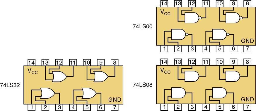
40 74 Series IC Packages


41 Logic Circuit using 74 Series x = AB + CD Possible Implementations # 1


42 Logic Circuit using 74 Series x = AB + CD Possible Implementations # 2

43 Boolean Theorems Th1: if any variable is ANDed with 0, the result must be 0. Th2: if any variable is ANDed with 1, the result must be itself Logic AND is just like ordinary multiplication!


44 Boolean Theorems Th3: A variable ANDed with itself is always equal to itself Th4: A variable ANDed with its complement is always 0

45 Boolean Theorems Th5: A variable ORed with 0 is always equal to itelf Th6: A variable ORed with 1 is always 1


46 Boolean Theorems Th7: A variable ORed with itself is always equal to itself Th8: A variable ORed with its complement is always 1
47 Commutative laws Multivariable Theorems Associative laws Distributive law

48 Multivariable Theorems Theorems (14) and (15) do not have counterparts in ordinary algebra. Each can be proved by - Trying all possible cases for x and y. Analysis table & factoring for Theorem (14)
49 DeMorgan s Theorems Each of DeMorgan s theorems can readily be proven by checking for all possible combinations of x and y.
 The alternative symbol for the NOR")
50 DeMorgan s Theorems Equivalent circuits implied by Theorem (16) The alternative symbol for the NOR function.
 The alternative symbol for the NOR")
51 DeMorgan s Theorems Equivalent circuits implied by Theorem (17) The alternative symbol for the NOR function.
52 References David M. Harris and Sarah L. Harris, Digital Design and Computer Architecture Thomas L. Floyd, Digital Fundamentals,11 th edition Ronald J. Tocci and Neal Widmer, Digital Systems Principles and Applications,11 th edition
53 Advanced Topic: CMOS Logic
54 NMOS Transistors in Series/Parallel Transistor switch controlled by its gate signal - NMOS switch closes when switch control input is high AND Y = X if A AND B OR Y = X if A OR B
55 PMOS Transistors in Series/Parallel PMOS switch closes when switch control input is low NOR Y = X if A AND B (A+B) NAND Y = X if A OR B (AB) 55
56 Complementary CMOS Logic Style Apply DeMorgan s Theorems A+B = A B AB = A + B The complementary gate is inverting AND = NAND + INV 56
57 Example: NAND Gate PDN: G = AB -> Conduction to GND PUN: F = A + B = AB -> Conduction to V DD G(In 1, In 2, In 3, ) = F (In 1, In 2, In 3, ) 57
58 Example: NOR Gate 58
59 Complex CMOS Gate 59
60 Constructing a Complex Gate F = D +A(B+C) Pull-down network Deriving the pull-up network hierarchically by identifying sub-nets Complete gate 60
Digital Systems Principles and Applications TWELFTH EDITION. 3-3 OR Operation With OR Gates. 3-4 AND Operations with AND gates
 Digital Systems Principles and Applications TWELFTH EDITION CHAPTER 3 Describing Logic Circuits Part -2 J. Bernardini 3-3 OR Operation With OR Gates An OR gate is a circuit with two or more inputs, whose
Chapter 3 Describing Logic Circuits Dr. Xu
 Chapter 3 Describing Logic Circuits Dr. Xu Chapter 3 Objectives Selected areas covered in this chapter: Operation of truth tables for AND, NAND, OR, and NOR gates, and the NOT (INVERTER) circuit. Boolean
CHAPTER 3 BASIC & COMBINATIONAL LOGIC CIRCUIT
 CHAPTER 3 BASIC & COMBINATIONAL LOGIC CIRCUIT CHAPTER CONTENTS 3.1 Introduction to Basic Gates 3.2 Analysing A Combinational Logic Circuit 3.3 Design A Combinational Logic Circuit From Boolean Expression
In this lecture: Lecture 3: Basic Logic Gates & Boolean Expressions
 In this lecture: Lecture 3: Basic Logic Gates & Boolean Expressions Dr Pete Sedcole Department of E&E Engineering Imperial College London http://cas.ee.ic.ac.uk/~nps/ (Floyd 3.1 3.6, 4.1) (Tocci 3.1 3.9)
2 Logic Gates THE INVERTER. A logic gate is an electronic circuit which makes logic decisions. It has one output and one or more inputs.
 2 Logic Gates A logic gate is an electronic circuit which makes logic decisions. It has one output and one or more inputs. THE INVERTER The inverter (NOT circuit) performs the operation called inversion
Practice 6: CMOS Digital Logic
 Practice 6: CMOS Digital Logic Digital Electronic Circuits Semester A 2012 The MOSFET as a Switch The MOSFET as a Switch We can look at the MOSFET as a Switch, passing the data between the diffusions when
ECE380 Digital Logic. Logic values as voltage levels
 ECE380 Digital Logic Implementation Technology: NMOS and PMOS Transistors, CMOS logic gates Dr. D. J. Jackson Lecture 13-1 Logic values as voltage levels V ss is the minimum voltage that can exist in the
This Figure here illustrates the operation for a 2-input OR gate for all four possible input combinations.
 Course: B.Sc. Applied Physical Science (Computer Science) Year & Sem.: IInd Year, Sem - IIIrd Subject: Computer Science Paper No.: IX Paper Title: Computer System Architecture Lecture No.: 5 Lecture Title:
ECE 334: Electronic Circuits Lecture 10: Digital CMOS Circuits
 Faculty of Engineering ECE 334: Electronic Circuits Lecture 10: Digital CMOS Circuits CMOS Technology Complementary MOS, or CMOS, needs both PMOS and NMOS FET devices for their logic gates to be realized
Subject: Analog and Digital Electronics Code:15CS32
 Subject: Analog and Digital Electronics Code:15CS32 Syllabus: The Basic Gates : Review of Basic Logic gates, Positive and Negative Logic, Introduction to HDL. Combinational Logic Circuits:Sum-of-Products
Digital Microelectronic Circuits ( ) CMOS Digital Logic. Lecture 6: Presented by: Adam Teman
 CMOS Digital Logic. Lecture 6: Presented by: Adam Teman") Digital Microelectronic Circuits (361-1-3021 ) Presented by: Adam Teman Lecture 6: CMOS Digital Logic 1 Last Lectures The CMOS Inverter CMOS Capacitance Driving a Load 2 This Lecture Now that we know all
Digital Microelectronic Circuits (361-1-3021 ) Presented by: Adam Teman Lecture 6: CMOS Digital Logic 1 Last Lectures The CMOS Inverter CMOS Capacitance Driving a Load 2 This Lecture Now that we know all
Logic Design I (17.341) Fall Lecture Outline
 Fall Lecture Outline") Logic Design I (17.341) Fall 2011 Lecture Outline Class # 07 October 31, 2011 / November 07, 2011 Dohn Bowden 1 Today s Lecture Administrative Main Logic Topic Homework 2 Course Admin 3 Administrative
Logic Design I (17.341) Fall 2011 Lecture Outline Class # 07 October 31, 2011 / November 07, 2011 Dohn Bowden 1 Today s Lecture Administrative Main Logic Topic Homework 2 Course Admin 3 Administrative
Shorthand Notation for NMOS and PMOS Transistors
 Shorthand Notation for NMOS and PMOS Transistors Terminal Voltages Mode of operation depends on V g, V d, V s V gs = V g V s V gd = V g V d V ds = V d V s = V gs - V gd Source and drain are symmetric diffusion
University of Technology
 University of Technology Lecturer: Dr. Sinan Majid Course Title: microprocessors 4 th year Lecture 7 & 8 NAND and XOR Implementations Combinational Design Procedure NAND-NAND & NOR-NOR Networks DeMorgan
Positive and Negative Logic
 Course: B.Sc. Applied Physical Science (Computer Science) Year & Sem.: IInd Year, Sem - IIIrd Subject: Computer Science Paper No.: IX Paper Title: Computer System Architecture Lecture No.: 4 Lecture Title:
Chapter 3 Digital Logic Structures
 Chapter 3 Digital Logic Structures Transistor: Building Block of Computers Microprocessors contain millions of transistors Intel Pentium 4 (2): 48 million IBM PowerPC 75FX (22): 38 million IBM/Apple PowerPC
EMT1250 LABORATORY EXPERIMENT. EXPERIMENT # 4: Combinational Logic Circuits. Name: Date:
 EXPERIMENT # 4: Combinational Logic Circuits Name: Date: Equipment/Parts Needed: 5V DC Power Supply Digital Trainer (Logic Probe) Breadboard DIP Switch 7400 NAND gate 7402 NOR gate 7404 Inverter 7408 AND
BOOLEAN ALGEBRA AND LOGIC FAMILIES
 C H A P T E R 7 Learning Objectives Unique Feature of Boolean Algebra Laws of Boolean Algebra Equivalent Switching Circuits DeMorgan s Theorem s The Sum-of-Products (SOP) Form The Standard SOP Form The
Chapter 3 Digital Logic Structures
 Chapter 3 Digital Logic Structures Transistor: Building Block of Computers Microprocessors contain millions of transistors Intel Pentium 4 (2000): 48 million IBM PowerPC 750FX (2002): 38 million IBM/Apple
ECE/CoE 0132: FETs and Gates
 ECE/CoE 0132: FETs and Gates Kartik Mohanram September 6, 2017 1 Physical properties of gates Over the next 2 lectures, we will discuss some of the physical characteristics of integrated circuits. We will
Chapter 1: Digital logic
 Chapter 1: Digital logic I. Overview In PHYS 252, you learned the essentials of circuit analysis, including the concepts of impedance, amplification, feedback and frequency analysis. Most of the circuits
Analysis procedure. To obtain the output Boolean functions from a logic diagram, proceed as follows:
 Combinational Logic Logic circuits for digital systems may be combinational or sequential. combinational circuit consists of input variables, logic gates, and output variables. 1 nalysis procedure To obtain
Function Table of an Odd-Parity Generator Circuit
 Implementation of an Odd-Parity Generator Circuit The first step in implementing any circuit is to represent its operation in terms of a Truth or Function table. The function table for an 8-bit data as
(CSC-3501) Lecture 6 (31 Jan 2008) Seung-Jong Park (Jay) CSC S.J. Park. Announcement
 Lecture 6 (31 Jan 2008) Seung-Jong Park (Jay) CSC S.J. Park. Announcement") Seung-Jong Park (Jay) http://www.csc.lsu.edu/~sjpark Computer Architecture (CSC-3501) Lecture 6 (31 Jan 2008) 1 Announcement 2 1 Reminder A logic circuit is composed of: Inputs Outputs Functional specification
Seung-Jong Park (Jay) http://www.csc.lsu.edu/~sjpark Computer Architecture (CSC-3501) Lecture 6 (31 Jan 2008) 1 Announcement 2 1 Reminder A logic circuit is composed of: Inputs Outputs Functional specification
Topic 6. CMOS Static & Dynamic Logic Gates. Static CMOS Circuit. NMOS Transistors in Series/Parallel Connection
 NMOS Transistors in Series/Parallel Connection Topic 6 CMOS Static & Dynamic Logic Gates Peter Cheung Department of Electrical & Electronic Engineering Imperial College London Transistors can be thought
Lecture 7: Digital Logic
 Lecture 7: Digital Logic Last time we introduced the concept of digital electronics i.e., one identifies a range of voltages with the value, and another range with the value But we didn t specify these
ECE Digital Logic Lecture 2. Digital Design Circuit Types: Combinational vs. Sequential
 ECE 74 - Digital Logic Lecture Circuit Types: Combinational vs. equential Lecture Transistors, witches, CMO Basic Logic Gates Boolean Equations Truth Table: w/o time or previous values Circuit Components:
ECE 2300 Digital Logic & Computer Organization
 ECE 2300 Digital Logic & Computer Organization Spring 2018 CMOS Logic Lecture 4: 1 NAND Logic Gate X Y (X Y) = NAND Using De Morgan s Law: (X Y) = X +Y X X X +Y = Y Y Also a NAND We can build circuits
Logic diagram: a graphical representation of a circuit
 LOGIC AND GATES Introduction to Logic (1) Logic diagram: a graphical representation of a circuit Each type of gate is represented by a specific graphical symbol Truth table: defines the function of a gate
Gates and Circuits 1
 1 Gates and Circuits Chapter Goals Identify the basic gates and describe the behavior of each Describe how gates are implemented using transistors Combine basic gates into circuits Describe the behavior
Lecture 15 Analysis of Combinational Circuits
 Lecture 15 Analysis of Combinational Circuits Designing Combinational Logic Circuits A logic circuit having 3 inputs, A, B, C will have its output HIGH only when a majority of the inputs are HIGH. Step
INTRODUCTION TO DIGITAL CONCEPT
 COURSE / CODE DIGITAL SYSTEM FUNDAMENTALS (ECE 421) DIGITAL ELECTRONICS FUNDAMENTAL (ECE 422) INTRODUCTION TO DIGITAL CONCEPT Digital and Analog Quantities Digital relates to data in the form of digits,
Asst. Prof. Thavatchai Tayjasanant, PhD. Power System Research Lab 12 th Floor, Building 4 Tel: (02)
") 2145230 Aircraft Electricity and Electronics Asst. Prof. Thavatchai Tayjasanant, PhD Email: taytaycu@gmail.com aycu@g a co Power System Research Lab 12 th Floor, Building 4 Tel: (02) 218-6527 1 Chapter
2145230 Aircraft Electricity and Electronics Asst. Prof. Thavatchai Tayjasanant, PhD Email: taytaycu@gmail.com aycu@g a co Power System Research Lab 12 th Floor, Building 4 Tel: (02) 218-6527 1 Chapter
Electronics. Digital Electronics
 Electronics Digital Electronics Introduction Unlike a linear, or analogue circuit which contains signals that are constantly changing from one value to another, such as amplitude or frequency, digital
COMPUTER ORGANIZATION & ARCHITECTURE DIGITAL LOGIC CSCD211- DEPARTMENT OF COMPUTER SCIENCE, UNIVERSITY OF GHANA
 COMPUTER ORGANIZATION & ARCHITECTURE DIGITAL LOGIC LOGIC Logic is a branch of math that tries to look at problems in terms of being either true or false. It will use a set of statements to derive new true
Lecture #1. Course Overview
 Lecture #1 OUTLINE Course overview Introduction: integrated circuits Analog vs. digital signals Lecture 1, Slide 1 Course Overview EECS 40: One of five EECS core courses (with 20, 61A, 61B, and 61C) introduces
Combinational logic. ! Regular logic: multiplexers, decoders, LUTs and FPGAs. ! Switches, basic logic and truth tables, logic functions
 Combinational logic! Switches, basic logic and truth tables, logic functions! Algebraic expressions to gates! Mapping to different gates! Discrete logic gate components (used in labs and 2)! Canonical
Odd-Prime Number Detector The table of minterms is represented. Table 13.1
 Odd-Prime Number Detector The table of minterms is represented. Table 13.1 Minterm A B C D E 1 0 0 0 0 1 3 0 0 0 1 1 5 0 0 1 0 1 7 0 0 1 1 1 11 0 1 0 1 1 13 0 1 1 0 1 17 1 0 0 0 1 19 1 0 0 1 1 23 1 0 1
Copyright The McGraw-Hill Companies, Inc. Permission required for reproduction or display. Computing Layers
 Chapter 3 Digital Logic Structures Original slides from Gregory Byrd, North Carolina State University Modified by Chris Wilcox, Sanjay Rajopadhye Colorado State University Computing Layers Problems Algorithms
Spiral 1 / Unit 8. Transistor Implementations CMOS Logic Gates
 18.1 Spiral 1 / Unit 8 Transistor Implementations CMOS Logic Gates 18.2 Spiral Content Mapping Spiral Theory Combinational Design Sequential Design System Level Design Implementation and Tools Project
Digital Logic Circuits
 Digital Logic Circuits Let s look at the essential features of digital logic circuits, which are at the heart of digital computers. Learning Objectives Understand the concepts of analog and digital signals
Name: Class: Date: 1. As more electronic systems have been designed using digital technology, devices have become smaller and less powerful.
 Name: Class: Date: DE Midterm Review 2 True/False Indicate whether the statement is true or false. 1. As more electronic systems have been designed using digital technology, devices have become smaller
A SUBSTRATE BIASED FULL ADDER CIRCUIT
 International Journal on Intelligent Electronic System, Vol. 8 No.. July 4 9 A SUBSTRATE BIASED FULL ADDER CIRCUIT Abstract Saravanakumar C., Senthilmurugan S.,, Department of ECE, Valliammai Engineering
Introduction to Digital Logic Missouri S&T University CPE 2210 Exam 1 Logistics
 Introduction to Digital Logic Missouri S&T University CPE 2210 Exam 1 Logistics Egemen K. Çetinkaya Egemen K. Çetinkaya Department of Electrical & Computer Engineering Missouri University of Science and
Digital Fundamentals. Logic gates
 Digital Fundamentals Logic gates Objectives Describe the operation of the inverter, the AND gate, and the OR gate Describe the operation of the NAND gate and the NOR gate Express the operation of the NOT,
ECE380 Digital Logic
 ECE38 Digital Logic Introduction Dr. D. J. Jackson Lecture - Digital hardware Logic circuits are used to build computer hardware as well as other products (digital hardware) Late 96 s and early 97 s saw
OBJECTIVE TYPE QUESTIONS FOR PRACTICAL EXAMINATION Subject : Electronics-I ( EC 112)
") OBJECTIVE TYPE QUESTIONS FOR PRACTICAL EXAMINATION Subject : Electronics-I ( EC 112) 1. Which mathematical notation specifies the condition of periodicity for a continuous time signal? a. x(t) = x( t +T)
OBJECTIVE TYPE QUESTIONS FOR PRACTICAL EXAMINATION Subject : Electronics-I ( EC 112) 1. Which mathematical notation specifies the condition of periodicity for a continuous time signal? a. x(t) = x( t +T)
UNIT-III GATE LEVEL DESIGN
 UNIT-III GATE LEVEL DESIGN LOGIC GATES AND OTHER COMPLEX GATES: Invert(nmos, cmos, Bicmos) NAND Gate(nmos, cmos, Bicmos) NOR Gate(nmos, cmos, Bicmos) The module (integrated circuit) is implemented in terms
Chapter 4 Combinational Logic Circuits
 Chapter 4 Combinational Logic Circuits Chapter 4 Objectives Selected areas covered in this chapter: Converting logic expressions to sum-of-products expressions. Boolean algebra and the Karnaugh map as
Formal Foundation of Digital Design
 Chapter 2: Switching Algebra and Logic Circuits 78 22 Digital Logic Design @ Department of Computer Engineering KKU. Formal Foundation of Digital Design In 854 George Boole published An investigation into
Digital Applications (CETT 1415) Credit: 4 semester credit hours (3 hours lecture, 4 hours lab) Prerequisite: CETT 1403 & CETT 1405
 Credit: 4 semester credit hours (3 hours lecture, 4 hours lab) Prerequisite: CETT 1403 & CETT 1405") Digital Applications () Credit: 4 semester credit hours (3 hours lecture, 4 hours lab) Prerequisite: CETT 1403 & CETT 1405 Course Description This course covers digital techniques and numbering systems,
Digital Applications () Credit: 4 semester credit hours (3 hours lecture, 4 hours lab) Prerequisite: CETT 1403 & CETT 1405 Course Description This course covers digital techniques and numbering systems,
DIGITAL CIRCUITS AND SYSTEMS ASSIGNMENTS 1 SOLUTIONS
 DIGITAL CIRCUITS AND SYSTEMS ASSIGNMENTS 1 SOLUTIONS 1. Analog signal varies continuously between two amplitudes over the given interval of time. Between these limits of amplitude and time, the signal
Lecture Summary Module 1 Switching Algebra and CMOS Logic Gates
 Lecture Summary Module 1 Switching Algebra and CMOS Logic Gates Learning Outcome: an ability to analyze and design CMOS logic gates Learning Objectives: 1-1. convert numbers from one base (radix) to another:
Digital Fundamentals
 Digital Fundamentals Tenth Edition Floyd hapter 5 Floyd, Digital Fundamentals, th ed 28 Pearson Education 29 Pearson Education, Upper Saddle River, NJ 7458. ll Rights Reserved ombinational Logic ircuits
Chapter 4 Combinational Logic Circuits
 Chapter 4 Combinational Logic Circuits Chapter 4 Objectives Selected areas covered in this chapter: Converting logic expressions to sum-of-products expressions. Boolean algebra and the Karnaugh map as
Exercise 2: OR/NOR Logic Functions
 Exercise 2: OR/NOR Logic Functions EXERCISE OBJECTIVE When you have completed this exercise, you will be able to determine the operation of an OR and a NOR logic gate. You will verify your results by generating
Transistor Digital Circuits
 Transistor Digital Circuits Switching Transistor Model (on) (on) T n T p Controlled switch model v CT > V CTex ; T- (on); i O > 0; v O 0 v CT < V Thn ; T- (off); i O = 0; v O = V PS v CT > V Thp ; T- (off);
2-Bit Magnitude Comparator Design Using Different Logic Styles
 International Journal of Engineering Science Invention ISSN (Online): 2319 6734, ISSN (Print): 2319 6726 Volume 2 Issue 1 ǁ January. 2013 ǁ PP.13-24 2-Bit Magnitude Comparator Design Using Different Logic
Lab 2 Revisited Exercise
 Lab 2 Revisited Exercise +15V 100k 1K 2N2222 Wire up led display Note the ground leads LED orientation 6.091 IAP 2008 Lecture 3 1 Comparator, Oscillator +5 +15 1k 2 V- 7 6 Vin 3 V+ 4 V o Notice that power
EE40 Lecture 35. Prof. Chang-Hasnain. 12/5/07 Reading: Ch 7, Supplementary Reader
 EE4 Lecture 35 2/5/7 Reading: Ch 7, Supplementary Reader EE4 all 26 Slide Week 5 OUTLINE Need for Input Controlled Pull-Up CMOS Inverter nalysis CMOS Voltage Transfer Characteristic Combinatorial logic
Introduction to CMOS VLSI Design (E158) Lecture 5: Logic
 Lecture 5: Logic") Harris Introduction to CMOS VLSI Design (E158) Lecture 5: Logic David Harris Harvey Mudd College David_Harris@hmc.edu Based on EE271 developed by Mark Horowitz, Stanford University MAH E158 Lecture 5 1
Harris Introduction to CMOS VLSI Design (E158) Lecture 5: Logic David Harris Harvey Mudd College David_Harris@hmc.edu Based on EE271 developed by Mark Horowitz, Stanford University MAH E158 Lecture 5 1
Objective Questions. (a) Light (b) Temperature (c) Sound (d) all of these
 Light (b) Temperature (c) Sound (d) all of these") Objective Questions Module 1: Introduction 1. Which of the following is an analog quantity? (a) Light (b) Temperature (c) Sound (d) all of these 2. Which of the following is a digital quantity? (a) Electrical
Objective Questions Module 1: Introduction 1. Which of the following is an analog quantity? (a) Light (b) Temperature (c) Sound (d) all of these 2. Which of the following is a digital quantity? (a) Electrical
ENG2410 Digital Design CMOS Technology. Fall 2017 S. Areibi School of Engineering University of Guelph
 ENG2410 Digital Design CMOS Technology Fall 2017 S. reibi School of Engineering University of Guelph The Transistor Revolution First transistor Bell Labs, 1948 Bipolar logic 1960 s Intel 4004 processor
DIGITAL ELECTRONICS. Methods & diagrams : 1 Graph plotting : - Tables & analysis : - Questions & discussion : 6 Performance : 3
 DIGITAL ELECTRONICS Marking scheme : Methods & diagrams : 1 Graph plotting : - Tables & analysis : - Questions & discussion : 6 Performance : 3 Aim: This experiment will investigate the function of the
Chapter 4: FLIP FLOPS. (Sequential Circuits) By: Siti Sabariah Hj. Salihin ELECTRICAL ENGINEERING DEPARTMENT EE 202 : DIGITAL ELECTRONICS 1
 By: Siti Sabariah Hj. Salihin ELECTRICAL ENGINEERING DEPARTMENT EE 202 : DIGITAL ELECTRONICS 1") Chapter 4: FLIP FLOPS (Sequential Circuits) By: Siti Sabariah Hj. Salihin ELECTRICAL ENGINEERING DEPARTMENT 1 CHAPTER 4 : FLIP FLOPS Programme Learning Outcomes, PLO Upon completion of the programme, graduates
Chapter 4: FLIP FLOPS (Sequential Circuits) By: Siti Sabariah Hj. Salihin ELECTRICAL ENGINEERING DEPARTMENT 1 CHAPTER 4 : FLIP FLOPS Programme Learning Outcomes, PLO Upon completion of the programme, graduates
Combinational Logic Design CH002
 Combinational Logic Design CH002 Figure 2.1 Circuit as a black box with inputs, outputs, and specifications Figure 2.2 Elements and nodes Figure 2.3 Combinational logic circuit Figure 2.4 Two OR implementations
Lecture 02: Digital Logic Review
 CENG 3420 Lecture 02: Digital Logic Review Bei Yu byu@cse.cuhk.edu.hk CENG3420 L02 Digital Logic. 1 Spring 2017 Review: Major Components of a Computer CENG3420 L02 Digital Logic. 2 Spring 2017 Review:
Digital Fundamentals
 Digital Fundamentals Tenth Edition Floyd Chapter 3 28 Pearson Education 29 Pearson Education, Upper Saddle River, NJ 7458. ll Rights Reserved The Inverter The inverter performs the oolean NOT operation.
Lecture 7: Components of Phase Locked Loop (PLL)
") Lecture 7: Components of Phase Locked Loop (PLL) CSCE 6933/5933 Instructor: Saraju P. Mohanty, Ph. D. NOTE: The figures, text etc included in slides are borrowed from various books, websites, authors pages,
Lecture 7: Components of Phase Locked Loop (PLL) CSCE 6933/5933 Instructor: Saraju P. Mohanty, Ph. D. NOTE: The figures, text etc included in slides are borrowed from various books, websites, authors pages,
Number system: the system used to count discrete units is called number. Decimal system: the number system that contains 10 distinguished
 Number system: the system used to count discrete units is called number system Decimal system: the number system that contains 10 distinguished symbols that is 0-9 or digits is called decimal system. As
Digital Fundamentals 8/29/2016. Summary. Summary. Floyd. Chapter 3 A X. The Inverter
 Digital Fundamentals Tenth Edition Floyd Chapter 3 The Inverter The inverter performs the oolean NOT operation. When the input is LOW, the output is HIGH; when the input is HIGH, the output is LOW. Input
1. Short answer questions. (30) a. What impact does increasing the length of a transistor have on power and delay? Why? (6)
 a. What impact does increasing the length of a transistor have on power and delay? Why? (6)") CSE 493/593 Test 2 Fall 2011 Solution 1. Short answer questions. (30) a. What impact does increasing the length of a transistor have on power and delay? Why? (6) Decreasing of W to make the gate slower,
CSE 493/593 Test 2 Fall 2011 Solution 1. Short answer questions. (30) a. What impact does increasing the length of a transistor have on power and delay? Why? (6) Decreasing of W to make the gate slower,
ECE 410: VLSI Design Course Lecture Notes (Uyemura textbook)
") ECE 410: VLSI Design Course Lecture Notes (Uyemura tetbook) Professor Fathi Salem Michigan State University We will be updating the notes this Semester. Lecture Notes Page 2.1 Electronics Revolution Age
ECE 410: VLSI Design Course Lecture Notes (Uyemura tetbook) Professor Fathi Salem Michigan State University We will be updating the notes this Semester. Lecture Notes Page 2.1 Electronics Revolution Age
ECE 471/571 The CMOS Inverter Lecture-6. Gurjeet Singh
 ECE 471/571 The CMOS Inverter Lecture-6 Gurjeet Singh NMOS-to-PMOS ratio,pmos are made β times larger than NMOS Sizing Inverters for Performance Conclusions: Intrinsic delay tp0 is independent of sizing
Gates and and Circuits
 Chapter 4 Gates and Circuits Chapter Goals Identify the basic gates and describe the behavior of each Describe how gates are implemented using transistors Combine basic gates into circuits Describe the
Power-Area trade-off for Different CMOS Design Technologies
 Power-Area trade-off for Different CMOS Design Technologies Priyadarshini.V Department of ECE Sri Vishnu Engineering College for Women, Bhimavaram dpriya69@gmail.com Prof.G.R.L.V.N.Srinivasa Raju Head
Exercise 1: AND/NAND Logic Functions
 Exercise 1: AND/NAND Logic Functions EXERCISE OBJECTIVE When you have completed this exercise, you will be able to determine the operation of an AND and a NAND logic gate. You will verify your results
EE 330 Lecture 42. Other Logic Styles Digital Building Blocks
 EE 330 Lecture 42 Other Logic Styles Digital Building Blocks Logic Styles Static CMOS Complex Logic Gates Pass Transistor Logic (PTL) Pseudo NMOS Dynamic Logic Domino Zipper Static CMOS Widely used Attractive
6.1 In this section, you will design (but NOT build) a circuit with 4 inputs,
 a circuit with 4 inputs,") EE 2449 Experiment 6 Jack Levine and Nancy Warter-Perez //208 CALIFORNIA STATE UNIVERSITY LOS ANGELES Department of Electrical and Computer Engineering EE-2449 Digital Logic Lab EXPERIMENT 6 COMBINATIONAL
EE 2449 Experiment 6 Jack Levine and Nancy Warter-Perez //208 CALIFORNIA STATE UNIVERSITY LOS ANGELES Department of Electrical and Computer Engineering EE-2449 Digital Logic Lab EXPERIMENT 6 COMBINATIONAL
Name EGR 2131 Lab #2 Logic Gates and Boolean Algebra Objectives Equipment and Components Part 1: Reading Pin Diagrams 7400 (TOP VIEW)
") Name EGR 23 Lab #2 Logic Gates and Boolean Algebra Objectives ) Become familiar with common logic-gate chips and their pin numbers. 2) Using breadboarded chips, investigate the behavior of NOT (Inverter),
Name EGR 23 Lab #2 Logic Gates and Boolean Algebra Objectives ) Become familiar with common logic-gate chips and their pin numbers. 2) Using breadboarded chips, investigate the behavior of NOT (Inverter),
Engr354: Digital Logic Circuits
 Engr354: Digital Logic Circuits Chapter 3: Implementation Technology Curtis Nelson Chapter 3 Overview In this chapter you will learn about: How transistors are used as switches; Integrated circuit technology;
Lecture 9 Transistors
 Lecture 9 Transistors Physics Transistor/transistor logic CMOS logic CA 1947 http://www.extremetech.com/extreme/164301-graphenetransistors-based-on-negative-resistance-could-spell-theend-of-silicon-and-semiconductors
Digital Applications (CETT 1415) Credit: 4 semester credit hours (3 hours lecture, 4 hours lab) Prerequisite: CETT 1403 & CETT 1405
 Credit: 4 semester credit hours (3 hours lecture, 4 hours lab) Prerequisite: CETT 1403 & CETT 1405") Digital Applications (CETT 1415) Credit: 4 semester credit hours (3 hours lecture, 4 hours lab) Prerequisite: CETT 1403 & CETT 1405 Course Description This course covers digital techniques and numbering
Digital Applications (CETT 1415) Credit: 4 semester credit hours (3 hours lecture, 4 hours lab) Prerequisite: CETT 1403 & CETT 1405 Course Description This course covers digital techniques and numbering
Dynamic Logic. Domino logic P-E logic NORA logic 2-phase logic Multiple O/P domino logic Cascode logic 11/28/2012 1
 Dynamic Logic Dynamic Circuits will be introduced and their performance in terms of power, area, delay, energy and AT 2 will be reviewed. We will review the following logic families: Domino logic P-E logic
EXPERIMENT NO 1 TRUTH TABLE (1)
") EPERIMENT NO AIM: To verify the Demorgan s theorems. APPARATUS REQUIRED: THEORY: Digital logic trainer and Patch cords. The digital signals are discrete in nature and can only assume one of the two values
EPERIMENT NO AIM: To verify the Demorgan s theorems. APPARATUS REQUIRED: THEORY: Digital logic trainer and Patch cords. The digital signals are discrete in nature and can only assume one of the two values
Digital Fundamentals 9/4/2017. Summary. Summary. Floyd. Chapter 3. The Inverter
 Digital Fundamentals Tenth Edition Floyd Chapter 3 29 Pearson Education, Upper 28 Pearson Saddle River, Education NJ 7458. ll Rights Reserved The Inverter The inverter performs the oolean NOT operation.
CMOS Circuits CONCORDIA VLSI DESIGN LAB
 CMOS Circuits 1 Combination and Sequential 2 Static Combinational Network CMOS Circuits Pull-up network-pmos Pull-down network-nmos Networks are complementary to each other When the circuit is dormant,
Fan in: The number of inputs of a logic gate can handle.
 Subject Code: 17333 Model Answer Page 1/ 29 Important Instructions to examiners: 1) The answers should be examined by key words and not as word-to-word as given in the model answer scheme. 2) The model
EE 42/100 Lecture 23: CMOS Transistors and Logic Gates. Rev A 4/15/2012 (10:39 AM) Prof. Ali M. Niknejad
 Prof. Ali M. Niknejad") A. M. Niknejad University of California, Berkeley EE 100 / 42 Lecture 23 p. 1/16 EE 42/100 Lecture 23: CMOS Transistors and Logic Gates ELECTRONICS Rev A 4/15/2012 (10:39 AM) Prof. Ali M. Niknejad University
A. M. Niknejad University of California, Berkeley EE 100 / 42 Lecture 23 p. 1/16 EE 42/100 Lecture 23: CMOS Transistors and Logic Gates ELECTRONICS Rev A 4/15/2012 (10:39 AM) Prof. Ali M. Niknejad University
Digital Fundamentals. Lab 4 EX-OR Circuits & Combinational Circuit Design
 Richland College School of Engineering & Technology Rev. 0 B. Donham Rev. 1 (7/2003) J. Horne Rev. 2 (1/2008) J. Bradbury Digital Fundamentals CETT 1425 Lab 4 EX-OR Circuits & Combinational Circuit Design
Multiple input gates. The AND gate
 Multiple input gates Inverters and buffers exhaust the possibilities for single-input gate circuits. What more can be done with a single logic signal but to buffer it or invert it? To explore more logic
EECS 150 Homework 4 Solutions Fall 2008
 Problem 1: You have a 100 MHz clock, and need to generate 3 separate clocks at different frequencies: 20 MHz, 1kHz, and 1Hz. How many flip flops do you need to implement each clock if you use: a) a ring
Electronics Basic CMOS digital circuits
 Electronics Basic CMOS digital circuits Prof. Márta Rencz, Gábor Takács, Dr. György Bognár, Dr. Péter G. Szabó BME DED October 21, 2014 1 / 30 Introduction The topics covered today: The inverter: the simplest
Introduction (concepts and definitions)
") Objectives: Introduction (digital system design concepts and definitions). Advantages and drawbacks of digital techniques compared with analog. Digital Abstraction. Synchronous and Asynchronous Systems.
Objectives: Introduction (digital system design concepts and definitions). Advantages and drawbacks of digital techniques compared with analog. Digital Abstraction. Synchronous and Asynchronous Systems.
(B) The simplest way to measure the light intensity is using a photodiode in the photoconductive mode:
 The simplest way to measure the light intensity is using a photodiode in the photoconductive mode:") PHY226 Electronics Final Preparation 1. Optoelectronics: LEDs and photodiodes (A) LEDs and photodiodes are essentially semi conductor diodes which can interact with electromagnetic waves. Explain why in
PHY226 Electronics Final Preparation 1. Optoelectronics: LEDs and photodiodes (A) LEDs and photodiodes are essentially semi conductor diodes which can interact with electromagnetic waves. Explain why in
EEE 301 Digital Electronics
 EEE 301 Digital Electronics Lecture 1 Course Contents Introduction to number systems and codes. Analysis and synthesis of digital logic circuits: Basic logic functions, Boolean algebra,combinational logic
Lecture 16. Complementary metal oxide semiconductor (CMOS) CMOS 1-1
 CMOS 1-1") Lecture 16 Complementary metal oxide semiconductor (CMOS) CMOS 1-1 Outline Complementary metal oxide semiconductor (CMOS) Inverting circuit Properties Operating points Propagation delay Power dissipation
Lecture 16 Complementary metal oxide semiconductor (CMOS) CMOS 1-1 Outline Complementary metal oxide semiconductor (CMOS) Inverting circuit Properties Operating points Propagation delay Power dissipation
Multiple Category Scope and Sequence: Scope and Sequence Report For Course Standards and Objectives, Content, Skills, Vocabulary
 Multiple Category Scope and Sequence: Scope and Sequence Report For Course Standards and Objectives, Content, Skills, Vocabulary Wednesday, August 20, 2014, 1:16PM Unit Course Standards and Objectives
Lecture 6: Electronics Beyond the Logic Switches Xufeng Kou School of Information Science and Technology ShanghaiTech University
 Lecture 6: Electronics Beyond the Logic Switches Xufeng Kou School of Information Science and Technology ShanghaiTech University EE 224 Solid State Electronics II Lecture 3: Lattice and symmetry 1 Outline
Digital Electronics Course Objectives
 Digital Electronics Course Objectives In this course, we learning is reported using Standards Referenced Reporting (SRR). SRR seeks to provide students with grades that are consistent, are accurate, and