Digital Fundamentals. Logic gates
|
|
|
- Lionel Singleton
- 5 years ago
- Views:
Transcription
1 Digital Fundamentals Logic gates
2 Objectives Describe the operation of the inverter, the AND gate, and the OR gate Describe the operation of the NAND gate and the NOR gate Express the operation of the NOT, AND, OR, NAND, and NOR gates with Boolean algebra Describe the operation of the exclusive-or and exclusive-nor gates Recognize and use both the distinctive shape logic gate symbols and the rectangular outline logic gate symbols of ANSI/IEEE Standard Construct timing diagrams showing the proper time relationships of inputs and outputs for the various logic gates Make basic comparisons between the major IC technologies - CMOS and TTL Explain how the different series within the CMOS and TTL families differ from each other Define propagation, delay time, power dissipation, speed-power product, and fan-out in relation to logic gates List specific fixed-function integrated circuit devices that contain the various logic gates Use each logic gate in simple applications Troubleshoot logic gates for opens and shorts by using the logic pulser and probe or the oscilloscope Describe the basic concepts of programmable logic Logic gates 2


3 Inverter Check out the file F03-02! Thruth table Logic gates 3


4 AND Gate Logic gates 4


5 Pulsed operation Logic gates 5

6 Logic expressions for an AND gate Logic gates 6

7 Enable/inhibit function with an AND gate AND works as a gate for the clock signal Logic gates 7


8 Seat belt alarm system Logic gates 8


9 OR Gate Logic gates 9

10 Logic gates 10
11 Logic expressions for an OR gate = = = = 1 Logic gates 11

12 Simplified intrusion detection Logic gates 12

13 NAND Gate Logic gates 13
14 Equivalent operations! Logic gates 14

15 Example Logic gates 15

16 Example Logic gates 16

17 Logic gates 17


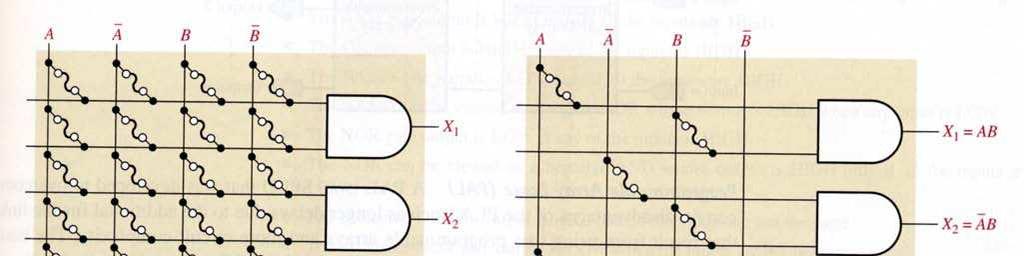
18 NOR Gate Logic gates 18
19 Equivalent operations! Logic gates 19
20 Example Logic gates 20

21 Logic gates 21
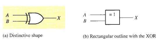


22 Exclusive-OR Gate Logic gates 22


23 Exclusive-NOR Gate Logic gates 23
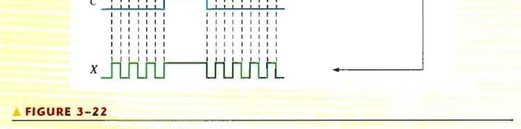
24 Pulsed operation Logic gates 24


25 Example Logic gates 25

26 Fixed-function logic: IC gates 5V 3V3 Logic gates 26

27 Logic gates 27


28 Fixed-function logic gates - Examples Logic gates 28

29 IC packages Logic gates 29


30 Pin configuration diagrams for some common fixed-function ICs Logic gates 30
31 Logic symbols for hex inverter Logic gates 31
32 Performance characteristics and parameters propagation delay time tphl and t PLH Logic gates 32
33 DC Supply voltage (marked V CC ) With CMOS gates you can use wider supply voltage range: 5V CMOS tolerates supply variations from 2V to 6V, 3V3 CMOS tolerates supply variations from 2V to 3.6V TTL requires stable supply voltage: maximum variation is +/- 10% (i.e. 4.5V to 5.5V) supply current with HIGH ouput Power dissipation (marked P D ) P D = V CC ICCH + 2 I CCL supply current with LOW ouput CMOS power dissipation is usually smaller compared to TTL, but the dissipation depends on frequency (power dissipation for TTL has no frequency dependence). Logic gates 33
 SPP = t P P D can be used to compared devices when considering both the speed and the")
34 Input and output logic levels 5V CMOS 5V CMOS TTL TTL 3.5V 4.4V 2V 2.4V 1.5V 0.33V 0.8V 0.4V Speed-power product (SPP) SPP = t P P D can be used to compared devices when considering both the speed and the dissipation power Logic gates 34
35 Fan-out and loading Fan-out is the number of inputs (of the same IC family) that can be connected to its output and still mantain the output voltage levels within specified limits. In CMOS circuits the fan-out is high but depends on frequency thru capacitive effects Logic gates 35


36 Comparison of propagation delay time and power in CMOS and TTL Logic gates 36


37 Logic gates 37


38 Logic gates 38
39 How to read datasheets and find the information you need Logic gates 39

40 Troubleshooting Internal failures An open TTL input acts as a HIGH level Logic gates 40


41 Troubleshooting a NAND gate for an open input Logic gates 41

42 Troubleshooting a NOR gate for an open input Logic gates 42


43 Example Logic gates 43
44 Example Logic gates 44


45 Example Logic gates 45

46 Logic gates 46


47 Programmable arrays OR array Logic gates 47

48 Programmable arrays AND array Logic gates 48


49 Classification of SPLDs PROM Logic gates 49
 Logic")
50 Classification of SPLDs PLA (programmable logic array) Logic gates 50
51 Classification of SPLDs PAL (programmable array logic) Logic gates 51

52 Classification of SPLDs GAL Logic gates 52


53 Summary Logic gates 53


54 Summary Logic gates 54
CMOS Digital Logic Design with Verilog. Chapter1 Digital IC Design &Technology
 CMOS Digital Logic Design with Verilog Chapter1 Digital IC Design &Technology Chapter Overview: In this chapter we study the concept of digital hardware design & technology. This chapter deals the standard
LSN 3 Logic Gates. ECT 224 Digital Computer Fundamentals. Department of Engineering Technology
 LSN 3 Logic Gates Department of Engineering Technology LSN 3 Inverter One input and one output Produces a compliment of the input Negation indicator Truth table Active low output In Out 0 1 1 0 Active
CS302 - Digital Logic Design Glossary By
 CS302 - Digital Logic Design Glossary By ABEL : Advanced Boolean Expression Language; a software compiler language for SPLD programming; a type of hardware description language (HDL) Adder : A digital
DIGITAL ELECTRONICS. Methods & diagrams : 1 Graph plotting : - Tables & analysis : - Questions & discussion : 6 Performance : 3
 DIGITAL ELECTRONICS Marking scheme : Methods & diagrams : 1 Graph plotting : - Tables & analysis : - Questions & discussion : 6 Performance : 3 Aim: This experiment will investigate the function of the
2 Logic Gates THE INVERTER. A logic gate is an electronic circuit which makes logic decisions. It has one output and one or more inputs.
 2 Logic Gates A logic gate is an electronic circuit which makes logic decisions. It has one output and one or more inputs. THE INVERTER The inverter (NOT circuit) performs the operation called inversion
IES Digital Mock Test
 . The circuit given below work as IES Digital Mock Test - 4 Logic A B C x y z (a) Binary to Gray code converter (c) Binary to ECESS- converter (b) Gray code to Binary converter (d) ECESS- To Gray code
Digital Fundamentals. Lab 4 EX-OR Circuits & Combinational Circuit Design
 Richland College School of Engineering & Technology Rev. 0 B. Donham Rev. 1 (7/2003) J. Horne Rev. 2 (1/2008) J. Bradbury Digital Fundamentals CETT 1425 Lab 4 EX-OR Circuits & Combinational Circuit Design
Name EGR 2131 Lab #2 Logic Gates and Boolean Algebra Objectives Equipment and Components Part 1: Reading Pin Diagrams 7400 (TOP VIEW)
") Name EGR 23 Lab #2 Logic Gates and Boolean Algebra Objectives ) Become familiar with common logic-gate chips and their pin numbers. 2) Using breadboarded chips, investigate the behavior of NOT (Inverter),
Name EGR 23 Lab #2 Logic Gates and Boolean Algebra Objectives ) Become familiar with common logic-gate chips and their pin numbers. 2) Using breadboarded chips, investigate the behavior of NOT (Inverter),
Course Outline Cover Page
 College of Micronesia FSM P.O. Box 159 Kolonia, Pohnpei Course Outline Cover Page Digital Electronics I VEE 135 Course Title Department and Number Course Description: This course provides the students
IC Logic Families. Wen-Hung Liao, Ph.D. 5/16/2001
 IC Logic Families Wen-Hung Liao, Ph.D. 5/16/2001 Digital IC Terminology Voltage Parameters: V IH (min): high-level input voltage, the minimum voltage level required for a logic 1 at an input. V IL (max):
INTEGRATED CIRCUITS. For a complete data sheet, please also download:
 INTEGRATED CIRCUITS DATA SHEET For a complete data sheet, please also download: The IC0 74HC/HCT/HCU/HCMOS Logic Family Specifications The IC0 74HC/HCT/HCU/HCMOS Logic Package Information The IC0 74HC/HCT/HCU/HCMOS
Chapter 2 Combinational Circuits
 Chapter 2 Combinational Circuits SKEE2263 Digital Systems Mun im/ismahani/izam {munim@utm.my,e-izam@utm.my,ismahani@fke.utm.my} February 23, 26 Why CMOS? Most logic design today is done on CMOS circuits
INTEGRATED CIRCUITS. For a complete data sheet, please also download:
 INTEGRATED CIRCUITS DATA SHEET For a complete data sheet, please also download: The IC06 74HC/HCT/HCU/HCMOS Logic Family Specifications The IC06 74HC/HCT/HCU/HCMOS Logic Package Information The IC06 74HC/HCT/HCU/HCMOS
Digital Fundamentals. Introductory Digital Concepts
 Digital Fundamentals Introductory Digital Concepts Objectives Explain the basic differences between digital and analog quantities Show how voltage levels are used to represent digital quantities Describe
Logic families (TTL, CMOS)
") Logic families (TTL, CMOS) When you work with digital IC's, you should be familiar, not only with their logical operation, but also with such operational properties as voltage levels, noise immunity, power
Logic families (TTL, CMOS) When you work with digital IC's, you should be familiar, not only with their logical operation, but also with such operational properties as voltage levels, noise immunity, power
Appendix B Page 1 54/74 FAMILIES OF COMPATIBLE TTL CIRCUITS PIN ASSIGNMENT (TOP VIEWS)
") Appendix B Page 1 54/74 FAMILIES OF COMPATIBLE TTL CIRCUITS PIN ASSIGNMENT (TOP VIEWS) See page 3 See page 3 See page 7 See page 14 See page 9 See page 16 See page 10 TEXAS INSTRUMENTS LTD have given their
Appendix B Page 1 54/74 FAMILIES OF COMPATIBLE TTL CIRCUITS PIN ASSIGNMENT (TOP VIEWS) See page 3 See page 3 See page 7 See page 14 See page 9 See page 16 See page 10 TEXAS INSTRUMENTS LTD have given their
Module-1: Logic Families Characteristics and Types. Table of Content
 1 Module-1: Logic Families Characteristics and Types Table of Content 1.1 Introduction 1.2 Logic families 1.3 Positive and Negative logic 1.4 Types of logic families 1.5 Characteristics of logic families
Digital Fundamentals 8/29/2016. Summary. Summary. Floyd. Chapter 3 A X. The Inverter
 Digital Fundamentals Tenth Edition Floyd Chapter 3 The Inverter The inverter performs the oolean NOT operation. When the input is LOW, the output is HIGH; when the input is HIGH, the output is LOW. Input
Digital Circuits and Operational Characteristics
 Digital Circuits and Operational Characteristics 1. DC Supply Voltage TTL based devices work with a dc supply of +5 Volts. TTL offers fast switching speed, immunity from damage due to electrostatic discharges.
Lecture 2: Digital Logic Basis
 Lecture 2: Digital Logic Basis Xufeng Kou School of Information Science and Technology ShanghaiTech University 1 Outline Truth Table Basic Logic Operation and Gates Logic Circuits NOR Gates and NAND Gates
Basic Characteristics of Digital ICs
 ECEN202 Section 2 Characteristics of Digital IC s Part 1: Specification of characteristics An introductory look at digital IC s: Logic families Basic construction and operation Operating characteristics
Gates and Circuits 1
 1 Gates and Circuits Chapter Goals Identify the basic gates and describe the behavior of each Describe how gates are implemented using transistors Combine basic gates into circuits Describe the behavior
This Figure here illustrates the operation for a 2-input OR gate for all four possible input combinations.
 Course: B.Sc. Applied Physical Science (Computer Science) Year & Sem.: IInd Year, Sem - IIIrd Subject: Computer Science Paper No.: IX Paper Title: Computer System Architecture Lecture No.: 5 Lecture Title:
74ACT00 QUAD 2-INPUT NAND GATE
 QUAD 2-INPUT NAND GATE HIGH SPEED: t PD = 5 ns (TYP.) at CC =5 LOW POWER DISSIPATION: I CC =4µA (MAX.) at T A =25 o C COMPATIBLE WITH TTL OUTPUTS IH =2(MIN), IL = 0.8 (MAX) 50Ω TRANSMISSION LINE DRIING
Engr354: Digital Logic Circuits
 Engr354: Digital Logic Circuits Chapter 3: Implementation Technology Curtis Nelson Chapter 3 Overview In this chapter you will learn about: How transistors are used as switches; Integrated circuit technology;
Chapter 4 Combinational Logic Circuits
 Chapter 4 Combinational Logic Circuits Chapter 4 Objectives Selected areas covered in this chapter: Converting logic expressions to sum-of-products expressions. Boolean algebra and the Karnaugh map as
Digital Fundamentals 9/4/2017. Summary. Summary. Floyd. Chapter 3. The Inverter
 Digital Fundamentals Tenth Edition Floyd Chapter 3 29 Pearson Education, Upper 28 Pearson Saddle River, Education NJ 7458. ll Rights Reserved The Inverter The inverter performs the oolean NOT operation.
EMT1250 LABORATORY EXPERIMENT. EXPERIMENT # 4: Combinational Logic Circuits. Name: Date:
 EXPERIMENT # 4: Combinational Logic Circuits Name: Date: Equipment/Parts Needed: 5V DC Power Supply Digital Trainer (Logic Probe) Breadboard DIP Switch 7400 NAND gate 7402 NOR gate 7404 Inverter 7408 AND
Exercise 1: Circuit Block Familiarization
 Exercise 1: Circuit Block Familiarization EXERCISE OBJECTIVE When you have completed this exercise, you will be able to locate and identify the circuit blocks and components on the DIGITAL LOGIC FUNDAMENTALS
M74HCT04. Hex inverter. Features. Description
 Hex inverter Features High speed: t PD = 11 ns (typ.) at =4.5V Low power dissipation: I CC = 1 μa (max.) at T A =25 C Compatible with TTL outputs: V IH = 2 V (min.) V IL = 0.8 V (max) Balanced propagation
Basic Logic Circuits
 Basic Logic Circuits Required knowledge Measurement of static characteristics of nonlinear circuits. Measurement of current consumption. Measurement of dynamic properties of electrical circuits. Definitions
74AC20M DUAL 4-INPUT NAND GATE
 DUAL 4-INPUT NAND GATE HIGH SPEED: t PD = 4 ns (TYP.) at V CC =5V LOW POWER DISSIPATION: I CC =4µA (MAX.) at T A =25 o C HIGH NOISE IMMUNITY: V NIH =V NIL = 28% V CC (MIN.) 50Ω TRANSMISSION LINE DRIVING
Chapter 4 Combinational Logic Circuits
 Chapter 4 Combinational Logic Circuits Chapter 4 Objectives Selected areas covered in this chapter: Converting logic expressions to sum-of-products expressions. Boolean algebra and the Karnaugh map as
Combinational Logic Circuits. Combinational Logic
 Combinational Logic Circuits The outputs of Combinational Logic Circuits are only determined by the logical function of their current input state, logic 0 or logic 1, at any given instant in time. The
The entire range of digital ICs is fabricated using either bipolar devices or MOS devices or a combination of the two. Bipolar Family DIODE LOGIC
 Course: B.Sc. Applied Physical Science (Computer Science) Year & Sem.: IInd Year, Sem - IIIrd Subject: Computer Science Paper No.: IX Paper Title: Computer System Architecture Lecture No.: 10 Lecture Title:
ECE380 Digital Logic
 ECE380 Digital Logic Implementation Technology: Standard Chips and Programmable Logic Devices Dr. D. J. Jackson Lecture 10-1 Standard chips A number of chips, each with a few logic gates, are commonly
Obsolete Product(s) - Obsolete Product(s)
 - Obsolete Product(s)") QUAD 2-INPUT NAND GATE HIGH SPEED: t PD = 12ns (TYP.) at V CC = 4.5V LOW POWER DISSIPATION: I CC = 1µA(MAX.) at T A =25 C COMPATIBLE WITH TTL OUTPUTS : V IH = 2V (MIN.) V IL = 0.8V (MAX) BALANCED PROPAGATION
QUAD 2-INPUT NAND GATE HIGH SPEED: t PD = 12ns (TYP.) at V CC = 4.5V LOW POWER DISSIPATION: I CC = 1µA(MAX.) at T A =25 C COMPATIBLE WITH TTL OUTPUTS : V IH = 2V (MIN.) V IL = 0.8V (MAX) BALANCED PROPAGATION
Number system: the system used to count discrete units is called number. Decimal system: the number system that contains 10 distinguished
 Number system: the system used to count discrete units is called number system Decimal system: the number system that contains 10 distinguished symbols that is 0-9 or digits is called decimal system. As
74ACT00B QUAD 2-INPUT NAND GATE
 QUAD 2-INPUT NAND GATE HIGH SPEED: t PD = 4.5ns (TYP.) at V CC = 5V LOW POWER DISSIPATION: I CC = 2µA(MAX.) at T A =25 C COMPATIBLE WITH TTL OUTPUTS V IH = 2V (MIN.), V IL = 0.8V (MAX.) 50Ω TRANSMISSION
Name: Class: Date: 1. As more electronic systems have been designed using digital technology, devices have become smaller and less powerful.
 Name: Class: Date: DE Midterm Review 2 True/False Indicate whether the statement is true or false. 1. As more electronic systems have been designed using digital technology, devices have become smaller
74V1T00CTR SINGLE 2-INPUT NAND GATE
 SINGLE 2-INPUT NAND GATE HIGH SPEED: t PD = 5.0ns (TYP.) at V CC =5V LOW POWER DISSIPATION: I CC =1µA(MAX.) at T A =25 C COMPATIBLE WITH TTL OUTPUTS: V IH =2V(MIN),V IL =0.8V(MAX) POWER DOWN PROTECTION
Obsolete Product(s) - Obsolete Product(s)
 - Obsolete Product(s)") SINGLE 2-INPUT NAND GATE HIGH SPEED: t PD = 5.0ns (TYP.) at V CC =5V LOW POWER DISSIPATION: I CC =1µA(MAX.) at T A =25 C COMPATIBLE WITH TTL OUTPUTS: V IH =2V(MIN),V IL =0.8V(MAX) POWER DOWN PROTECTION
SINGLE 2-INPUT NAND GATE HIGH SPEED: t PD = 5.0ns (TYP.) at V CC =5V LOW POWER DISSIPATION: I CC =1µA(MAX.) at T A =25 C COMPATIBLE WITH TTL OUTPUTS: V IH =2V(MIN),V IL =0.8V(MAX) POWER DOWN PROTECTION
Classification of Digital Circuits
 Classification of Digital Circuits Combinational logic circuits. Output depends only on present input. Sequential circuits. Output depends on present input and present state of the circuit. Combinational
Module -18 Flip flops
 1 Module -18 Flip flops 1. Introduction 2. Comparison of latches and flip flops. 3. Clock the trigger signal 4. Flip flops 4.1. Level triggered flip flops SR, D and JK flip flops 4.2. Edge triggered flip
Fan in: The number of inputs of a logic gate can handle.
 Subject Code: 17333 Model Answer Page 1/ 29 Important Instructions to examiners: 1) The answers should be examined by key words and not as word-to-word as given in the model answer scheme. 2) The model
2009 Spring CS211 Digital Systems & Lab 1 CHAPTER 3: TECHNOLOGY (PART 2)
") 1 CHAPTER 3: IMPLEMENTATION TECHNOLOGY (PART 2) Whatwillwelearninthischapter? we learn in this 2 How transistors operate and form simple switches CMOS logic gates IC technology FPGAs and other PLDs Basic
1 CHAPTER 3: IMPLEMENTATION TECHNOLOGY (PART 2) Whatwillwelearninthischapter? we learn in this 2 How transistors operate and form simple switches CMOS logic gates IC technology FPGAs and other PLDs Basic
M74HC4049TTR HEX BUFFER/CONVERTER (INVERTER)
") HEX BUFFER/CONVERTER (INVERTER) HIGH SPEED: t PD = 8ns (TYP.) at V CC =6V LOW POWER DISSIPATION: I CC = 1µA(MAX.) at T A =25 C HIGH NOISE IMMUNITY: V NIH = V NIL = 28 % V CC (MIN.) SYMMETRICAL OUTPUT IMPEDANCE:
HEX BUFFER/CONVERTER (INVERTER) HIGH SPEED: t PD = 8ns (TYP.) at V CC =6V LOW POWER DISSIPATION: I CC = 1µA(MAX.) at T A =25 C HIGH NOISE IMMUNITY: V NIH = V NIL = 28 % V CC (MIN.) SYMMETRICAL OUTPUT IMPEDANCE:
SN55451B, SN55452B, SN55453B, SN55454B SN75451B, SN75452B, SN75453B, SN75454B DUAL PERIPHERAL DRIVERS
 PERIPHERAL DRIVERS FOR HIGH-CURRENT SWITCHING AT VERY HIGH SPEEDS Characterized for Use to 00 ma High-Voltage Outputs No Output Latch-Up at 0 V (After Conducting 00 ma) High-Speed Switching Circuit Flexibility
INTEGRATED-CIRCUIT LOGIC FAMILIES
 C H A P T E R 8 INTEGRATED-CIRCUIT LOGIC FAMILIES OUTLINE 8-1 Digital IC Terminology 8-2 The TTL Logic Family 8-3 TTL Data Sheets 8-4 TTL Series Characteristics 8-5 TTL Loading and Fan-Out 8-6 Other TTL
Number of Lessons:155 #14B (P) Electronics Technology with Digital and Microprocessor Laboratory Completion Time: 42 months
 Electronics Technology with Digital and Microprocessor Laboratory Completion Time: 42 months") PROGRESS RECORD Study your lessons in the order listed below. Number of Lessons:155 #14B (P) Electronics Technology with Digital and Microprocessor Laboratory Completion Time: 42 months 1 2330A Current
PROGRESS RECORD Study your lessons in the order listed below. Number of Lessons:155 #14B (P) Electronics Technology with Digital and Microprocessor Laboratory Completion Time: 42 months 1 2330A Current
Positive and Negative Logic
 Course: B.Sc. Applied Physical Science (Computer Science) Year & Sem.: IInd Year, Sem - IIIrd Subject: Computer Science Paper No.: IX Paper Title: Computer System Architecture Lecture No.: 4 Lecture Title:
FAMILIARIZATION WITH DIGITAL PULSE AND MEASUREMENTS OF THE TRANSIENT TIMES
 EXPERIMENT 1 FAMILIARIZATION WITH DIGITAL PULSE AND MEASUREMENTS OF THE TRANSIENT TIMES REFERENCES Analysis and Design of Digital Integrated Circuits, Hodges and Jackson, pages 6-7 Experiments in Microprocessors
Lecture Summary Module 1 Switching Algebra and CMOS Logic Gates
 Lecture Summary Module 1 Switching Algebra and CMOS Logic Gates Learning Outcome: an ability to analyze and design CMOS logic gates Learning Objectives: 1-1. convert numbers from one base (radix) to another:
74LVCE1G00 SINGLE 2 INPUT POSITIVE NAND GATE. Description. Pin Assignments NEW PRODUCT. Features. Applications
 Description Pin Assignments The is a single 2-input positive NAND gate with a standard totem pole output. The device is designed for operation with a power supply range of 1.4V to 5.5V. The inputs are
Obsolete Product(s) - Obsolete Product(s)
 - Obsolete Product(s)") HEX INVERTER (SINGLE STATE) HIGH SPEED: t PD = 5ns (TYP.) at V CC = 6V LOW POWER DISSIPATION: I CC = 1µA(MAX.) at T A =25 C HIGH NOISE IMMUNITY: V NIH = V NIL = 10% V CC (MIN.) SYMMETRICAL OUTPUT IMPEDANCE:
HEX INVERTER (SINGLE STATE) HIGH SPEED: t PD = 5ns (TYP.) at V CC = 6V LOW POWER DISSIPATION: I CC = 1µA(MAX.) at T A =25 C HIGH NOISE IMMUNITY: V NIH = V NIL = 10% V CC (MIN.) SYMMETRICAL OUTPUT IMPEDANCE:
Chapter 6 DIFFERENT TYPES OF LOGIC GATES
 Chapter 6 DIFFERENT TYPES OF LOGIC GATES Lesson 9 CMOS gates Ch06L9-"Digital Principles and Design", Raj Kamal, Pearson Education, 2006 2 Outline CMOS (n-channel based MOSFETs based circuit) CMOS Features
M74HC10TTR TRIPLE 3-INPUT NAND GATE
 TRIPLE 3-INPUT NAND GATE HIGH SPEED: t PD = 8ns (TYP.) at V CC = 6V LOW POWER DISSIPATION: I CC = 1µA(MAX.) at T A =25 C HIGH NOISE IMMUNITY: V NIH = V NIL = 28 % V CC (MIN.) SYMMETRICAL OUTPUT IMPEDANCE:
Obsolete Product(s) - Obsolete Product(s)
 - Obsolete Product(s)") QUAD 2-INPUT NAND GATE HIGH SPEED: t PD = 8ns (TYP.) at V CC = 6V LOW POWER DISSIPATION: I CC = 1µA(MAX.) at T A =25 C HIGH NOISE IMMUNITY: V NIH = V NIL = 28 % V CC (MIN.) SYMMETRICAL OUTPUT IMPEDANCE:
QUAD 2-INPUT NAND GATE HIGH SPEED: t PD = 8ns (TYP.) at V CC = 6V LOW POWER DISSIPATION: I CC = 1µA(MAX.) at T A =25 C HIGH NOISE IMMUNITY: V NIH = V NIL = 28 % V CC (MIN.) SYMMETRICAL OUTPUT IMPEDANCE:
74VHCT00ATTR QUAD 2-INPUT NAND GATE
 QUAD 2-INPUT NAND GATE HIGH SPEED: t PD = 5 ns (TYP.) at V CC = 5V LOW POWER DISSIPATION: I CC = 2 µa (MAX.) at T A =25 C COMPATIBLE WITH TTL OUTPUTS: V IH = 2V (MIN.), V IL = 0.8V (MAX) POWER DOWN PROTECTION
1.) If a 3 input NOR gate has eight input possibilities, how many of those possibilities result in a HIGH output? (a.) 1 (b.) 2 (c.) 3 (d.) 7 (e.
 If a 3 input NOR gate has eight input possibilities, how many of those possibilities result in a HIGH output? (a.) 1 (b.) 2 (c.) 3 (d.) 7 (e.") Name: Multiple Choice 1.) If a 3 input NOR gate has eight input possibilities, how many of those possibilities result in a HIGH output? (a.) 1 (b.) 2 (c.) 3 (d.) 7 (e.) 8 2.) The output of an OR gate with
Name: Multiple Choice 1.) If a 3 input NOR gate has eight input possibilities, how many of those possibilities result in a HIGH output? (a.) 1 (b.) 2 (c.) 3 (d.) 7 (e.) 8 2.) The output of an OR gate with
54ACT11020, 74ACT11020 DUAL 4-INPUT POSITIVE-NAND GATES
 Inputs Are TTL-Voltage Compatible Flow-Through Architecture to Optimize PCB Layout Center-Pin V CC and GND Configurations to Minimize High-Speed Switching Noise EPIC (Enhanced-Performance Implanted CMOS)
M74HCT174TTR HEX D-TYPE FLIP FLOP WITH CLEAR
 HEX D-TYPE FLIP FLOP WITH CLEAR HIGH SPEED : f MAX = 56MHz (TYP.) at V CC = 4.5V LOW POWER DISSIPATION: I CC =4µA(MAX.) at T A =25 C COMPATIBLE WITH TTL OUTPUTS : V IH = 2V (MIN.) V IL = 0.8V (MAX) SYMMETRICAL
Digital Fundamentals
 Digital Fundamentals Tenth Edition Floyd Chapter 3 28 Pearson Education 29 Pearson Education, Upper Saddle River, NJ 7458. ll Rights Reserved The Inverter The inverter performs the oolean NOT operation.
ENGINEERING TRIPOS PART II A ELECTRICAL AND INFORMATION ENGINEERING TEACHING LABORATORY EXPERIMENT 3B2-B DIGITAL INTEGRATED CIRCUITS
 ENGINEERING TRIPOS PART II A ELECTRICAL AND INFORMATION ENGINEERING TEACHING LABORATORY EXPERIMENT 3B2-B DIGITAL INTEGRATED CIRCUITS OBJECTIVES : 1. To interpret data sheets supplied by the manufacturers
M74HCT02TTR QUAD 2-INPUT NOR GATE
 QUAD 2-INPUT NOR GATE HIGH SPEED: t PD = 15 ns (TYP.) at V CC = 4.5V LOW POWER DISSIPATION: I CC = 1µA(MAX.) at T A =25 C COMPATIBLE WITH TTL OUTPUTS : V IH = 2V (MIN.) V IL = 0.8V (MAX) BALANCED PROPAGATION
ua9637ac DUAL DIFFERENTIAL LINE RECEIVER
 ua967ac Meets or Exceeds the Requirements of ANSI Standards EIA/TIA--B and EIA/TIA--B and ITU Recommendations V. and V. Operates From Single -V Power Supply Wide Common-Mode Voltage Range High Input Impedance
Chapter 6 DIFFERENT TYPES OF LOGIC GATES
 Chapter 6 DIFFERENT TYPES OF LOGIC GATES Lesson 8 NMOS gates Ch06L8-"Digital Principles and Design", Raj Kamal, Pearson Education, 2006 2 Outline NMOS (n-channel based MOSFETs based circuit) NMOS Features
Analysis procedure. To obtain the output Boolean functions from a logic diagram, proceed as follows:
 Combinational Logic Logic circuits for digital systems may be combinational or sequential. combinational circuit consists of input variables, logic gates, and output variables. 1 nalysis procedure To obtain
Code No: R Set No. 1
 Code No: R05310402 Set No. 1 1. (a) What are the parameters that are necessary to define the electrical characteristics of CMOS circuits? Mention the typical values of a CMOS NAND gate. (b) Design a CMOS
Lecture 02: Logic Families. R.J. Harris & D.G. Bailey
 Lecture 02: Logic Families R.J. Harris & D.G. Bailey Objectives Show how diodes can be used to form logic gates (Diode logic). Explain the need for introducing transistors in the output (DTL and TTL).
74V1G00CTR SINGLE 2-INPUT NAND GATE
 SINGLE 2-INPUT NAND GATE HIGH SPEED: t PD = 3.7ns (TYP.) at V CC =5V LOW POWER DISSIPATION: I CC =1µA(MAX.) at T A =25 C HIGH NOISE IMMUNITY: V NIH =V NIL = 28% V CC (MIN.) POWER DOWN PROTECTION ON INPUTS
M74HC51TTR DUAL 2 WIDE 2 INPUT AND/OR INVERT GATE
 DUAL 2 WIDE 2 INPUT AND/OR INVERT GATE HIGH SPEED: t PD = 11ns (TYP.) at V CC = 6V LOW POWER DISSIPATION: I CC = 1µA(MAX.) at T A =25 C HIGH NOISE IMMUNITY: V NIH = V NIL = 28 % V CC (MIN.) SYMMETRICAL
Philips Semiconductors Programmable Logic Devices
 DESCRIPTION The PLD is a high speed, combinatorial Programmable Logic Array. The Philips Semiconductors state-of-the-art Oxide Isolated Bipolar fabrication process is employed to produce maximum propagation
74LVX132TTR LOW VOLTAGE CMOS QUAD 2-INPUT SCHMITT NAND GATE WITH 5V TOLERANT INPUTS
 LOW VOLTAGE CMOS QUAD 2-INPUT SCHMITT NAND GATE WITH 5V TOLERANT INPUTS HIGH SPEED : t PD = 5.9ns (TYP.) at V CC = 3.3V 5V TOLERANT INPUTS LOW POWER DISSIPATION: I CC = 2 µa (MAX.) at T A =25 C TYPICAL
Obsolete Product(s) - Obsolete Product(s)
 - Obsolete Product(s)") SINGLE POSITIVE EDGE TRIGGERED D-TYPE FLIP-FLOP HIGH SPEED: f MAX = 180MHz (TYP.) at V CC =5V LOW POWER DISSIPATION: I CC =1µA(MAX.) at T A =25 C COMPATIBLE WITH TTL OUTPUTS: V IH =2V(MIN),V IL =0.8V(MAX)
SINGLE POSITIVE EDGE TRIGGERED D-TYPE FLIP-FLOP HIGH SPEED: f MAX = 180MHz (TYP.) at V CC =5V LOW POWER DISSIPATION: I CC =1µA(MAX.) at T A =25 C COMPATIBLE WITH TTL OUTPUTS: V IH =2V(MIN),V IL =0.8V(MAX)
MM74HC86 Quad 2-Input Exclusive OR Gate
 MM74HC86 Quad 2-Input Exclusive OR Gate Features Typical Propagation Delay: 9ns Wide Operating oltage Range: 2 6 Low Input Current: 1mA Maximum Low Quiescent Current: 20mA Max. (74 Series) Output Drive
M74HCT164TTR 8 BIT SIPO SHIFT REGISTER
 8 BIT SIPO SHIFT REGISTER HIGH SPEED: t PD = 24 ns (TYP.) at V CC = 4.5V LOW POWER DISSIPATION: I CC = 4µA(MAX.) at T A =25 C COMPATIBLE WITH TTL OUTPUTS : V IH = 2V (MIN.) V IL = 0.8V (MAX) BALANCED PROPAGATION
SN54LS06, SN74LS06, SN74LS16 HEX INVERTER BUFFERS/DRIVERS WITH OPEN-COLLECTOR HIGH-VOLTAGE OUTPUTS
 Convert TTL Voltage Levels to MOS Levels High Sink-Current Capability Clamping Diodes Simplify System Design Open-Collector Driver for Indicator Lamps and Relays s Fully Compatible With Most TTL Circuits
74LVQ14 LOW VOLTAGE CMOS HEX SCHMITT INVERTER
 LOW VOLTAGE CMOS HEX SCHMITT INVERTER HIGH SPEED: t PD = 6 ns (TYP.) at V CC = 3.3 V HYSTERESIS INPUT VOLTAGE: V H = 650mV (TYP.) at V CC = 3.0 V COMPATIBLE WITH TTL OUTPUTS LOW POWER DISSIPATION: I CC
Digital Fundamentals A Systems Approach Thomas L. Floyd First Edition
 Digital Fundamentals Systems pproach Thomas L. Floyd First Edition Pearson Education Limited Edinburgh Gate Harlow Essex M20 2JE England and ssociated ompanies throughout the world Visit us on the World
Preface... iii. Chapter 1: Diodes and Circuits... 1
 Table of Contents Preface... iii Chapter 1: Diodes and Circuits... 1 1.1 Introduction... 1 1.2 Structure of an Atom... 2 1.3 Classification of Solid Materials on the Basis of Conductivity... 2 1.4 Atomic
Digital Systems Principles and Applications TWELFTH EDITION. 3-3 OR Operation With OR Gates. 3-4 AND Operations with AND gates
 Digital Systems Principles and Applications TWELFTH EDITION CHAPTER 3 Describing Logic Circuits Part -2 J. Bernardini 3-3 OR Operation With OR Gates An OR gate is a circuit with two or more inputs, whose
M74HCT574TTR OCTAL D-TYPE FLIP FLOP WITH 3 STATE OUTPUT NON INVERTING
 OCTAL D-TYPE FLIP FLOP WITH 3 STATE OUTPUT NON INVERTING HIGH SPEED: f MAX = 50MHz (TYP.) at V CC = 4.5V LOW POWER DISSIPATION: I CC = 4µA(MAX.) at T A =25 C COMPATIBLE WITH TTL OUTPUTS : V IH = 2V (MIN.)
74AC10B TRIPLE 3-INPUT NAND GATE
 TRIPLE 3-INPUT NAND GATE HIGH SPEED: t PD = 4ns (TYP.) at V CC = 5V LOW POWER DISSIPATION: I CC = 2µA(MAX.) at T A =25 C HIGH NOISE IMMUNITY: V NIH = V NIL = 28 % V CC (MIN.) 50Ω TRANSMISSION LINE DRIVING
74AC14, 74ACT14 Hex Inverter with Schmitt Trigger Input
 74AC14, 74ACT14 Hex Inverter with Schmitt Trigger Input Features I CC reduced by 50% Outputs source/sink 24mA 74ACT14 has TTL-compatible inputs Ordering Information Order Number General Description Package
74AC00B QUAD 2-INPUT NAND GATE
 QUAD 2-INPUT NAND GATE HIGH SPEED: t PD = 4ns (TYP.) at V CC = 5V LOW POWER DISSIPATION: I CC = 2µA(MAX.) at T A =25 C HIGH NOISE IMMUNITY: V NIH = V NIL = 28 % V CC (MIN.) 50Ω TRANSMISSION LINE DRIVING
74LVX04TTR LOW VOLTAGE CMOS HEX INVERTER WITH 5V TOLERANT INPUTS
 LOW OLTAGE CMOS HEX INERTER WITH 5 TOLERANT INPUTS HIGH SPEED : t PD = 4.1ns (TYP.) at CC = 3.3 5 TOLERANT INPUTS INPUT OLTAGE LEEL : IL =0.8, IH =2 at CC =3 LOW POWER DISSIPATION: I CC = 2 µa (MAX.) at
Quad 2-Input NAND Gate High-Voltage Silicon-Gate CMOS
 TECHNICAL DATA Quad 2-Input NAND Gate High-oltage Silicon-Gate CMOS The NAND gates provide the system designer with direct emplementation of the NAND function. Operating oltage Range:.0 to 18 Maximum input
Chapter 15 Integrated Circuits
 Chapter 15 Integrated Circuits SKEE1223 Digital Electronics Mun im/arif/izam FKE, Universiti Teknologi Malaysia December 8, 2015 Overview 1 Basic IC Characteristics Packaging Logic Families Datasheets
Department of EECS. University of California, Berkeley. Logic gates. September 1 st 2001
 Department of EECS University of California, Berkeley Logic gates Bharathwaj Muthuswamy and W. G. Oldham September 1 st 2001 1. Introduction This lab introduces digital logic. You use commercially available
Digital Applications (CETT 1415) Credit: 4 semester credit hours (3 hours lecture, 4 hours lab) Prerequisite: CETT 1403 & CETT 1405
 Credit: 4 semester credit hours (3 hours lecture, 4 hours lab) Prerequisite: CETT 1403 & CETT 1405") Digital Applications () Credit: 4 semester credit hours (3 hours lecture, 4 hours lab) Prerequisite: CETT 1403 & CETT 1405 Course Description This course covers digital techniques and numbering systems,
Digital Applications () Credit: 4 semester credit hours (3 hours lecture, 4 hours lab) Prerequisite: CETT 1403 & CETT 1405 Course Description This course covers digital techniques and numbering systems,
HCF4010B HEX BUFFER/CONVERTER (NON INVERTING)
") HEX BUFFER/CONVERTER (NON INVERTING) PROPAGATION DELAY TIME t PD = 40ns (TYP.) at V DD = 10V C L = 50pF HIGH TO LOW LEVEL LOGIC CONVERSION MULTIPLEXER: 1 TO 6 OR 6 TO 1 HIGH "SINK" AND "SOURCE" CURRENT
HEX BUFFER/CONVERTER (NON INVERTING) PROPAGATION DELAY TIME t PD = 40ns (TYP.) at V DD = 10V C L = 50pF HIGH TO LOW LEVEL LOGIC CONVERSION MULTIPLEXER: 1 TO 6 OR 6 TO 1 HIGH "SINK" AND "SOURCE" CURRENT
TC7WH04FU,TC7WH04FK TC7WH04FU/FK. Triple Inverter. Features. Marking. Pin Assignment (top view)
") TOSHIBA CMOS Digital Integrated Circuit Silicon Monolithic TC7WH04FU,TC7WH04FK TC7WH04FU/FK Triple Inverter The TC7WH04 is an advanced high speed CMOS Inverter fabricated with silicon gate CMOS technology.
TOSHIBA CMOS Digital Integrated Circuit Silicon Monolithic TC7WH04FU,TC7WH04FK TC7WH04FU/FK Triple Inverter The TC7WH04 is an advanced high speed CMOS Inverter fabricated with silicon gate CMOS technology.
Digital Logic Circuits
 Digital Logic Circuits Let s look at the essential features of digital logic circuits, which are at the heart of digital computers. Learning Objectives Understand the concepts of analog and digital signals
74ACT373 OCTAL D-TYPE LATCH WITH 3 STATE OUTPUT NON INVERTING
 OCTAL D-TYPE LATCH WITH 3 STATE OUTPUT NON INVERTING HIGH SPEED: t PD = 6 ns (TYP.) at V CC =5V LOW POWER DISSIPATION: I CC =8µA (MAX.) at T A =25 o C COMPATIBLE WITH TTL OUTPUTS V IH =2V(MIN),V IL = 0.8V
In this lecture: Lecture 8: ROM & Programmable Logic Devices
 In this lecture: Lecture 8: ROM Programmable Logic Devices Dr Pete Sedcole Department of EE Engineering Imperial College London http://caseeicacuk/~nps/ (Floyd, 3 5, 3) (Tocci 2, 24, 25, 27, 28, 3 34)
Obsolete Product(s) - Obsolete Product(s)
 - Obsolete Product(s)") HEX INVERTER (OPEN DRAIN) HIGH SPEED: t PD = 10ns (TYP.) at V CC = 6V LOW POWER DISSIPATION: I CC = 1µA(MAX.) at T A =25 C HIGH NOISE IMMUNITY: V NIH = V NIL = 28 % V CC (MIN.) WIDE OPERATING VOLTAGE RANGE:
HEX INVERTER (OPEN DRAIN) HIGH SPEED: t PD = 10ns (TYP.) at V CC = 6V LOW POWER DISSIPATION: I CC = 1µA(MAX.) at T A =25 C HIGH NOISE IMMUNITY: V NIH = V NIL = 28 % V CC (MIN.) WIDE OPERATING VOLTAGE RANGE:
74VHC20 DUAL 4-INPUT NAND GATE
 DUAL 4-INPUT NAND GATE HIGH SPEED: t PD = 3.3 ns (TYP.) at V CC = 5V LOW POWER DISSIPATION: I CC = 2 µa (MAX.) at T A =25 C HIGH NOISE IMMUNITY: V NIH = V NIL = 28% V CC (MIN.) POWER DOWN PROTECTION ON
Logic Families. A-PDF Split DEMO : Purchase from to remove the watermark. 5.1 Logic Families Significance and Types. 5.1.
 A-PDF Split DEMO : Purchase from www.a-pdf.com to remove the watermark 5 Logic Families Digital integrated circuits are produced using several different circuit configurations and production technologies.
M74HCT244TTR OCTAL BUS BUFFER WITH 3 STATE OUTPUTS (NON INVERTED)
") OCTAL BUS BUFFER WITH 3 STATE OUTPUTS (NON INVERTED) HIGH SPEED: t PD = 15 ns (TYP.) at V CC = 4.5V LOW POWER DISSIPATION: I CC = 4µA(MAX.) at T A =25 C COMPATIBLE WITH TTL OUTPUTS : V IH = 2V (MIN.) V
OCTAL BUS BUFFER WITH 3 STATE OUTPUTS (NON INVERTED) HIGH SPEED: t PD = 15 ns (TYP.) at V CC = 4.5V LOW POWER DISSIPATION: I CC = 4µA(MAX.) at T A =25 C COMPATIBLE WITH TTL OUTPUTS : V IH = 2V (MIN.) V