Chapter 4 Combinational Logic Circuits
|
|
|
- Ethel Butler
- 5 years ago
- Views:
Transcription
1 Chapter 4 Combinational Logic Circuits
2 Chapter 4 Objectives Selected areas covered in this chapter: Converting logic expressions to sum-of-products expressions. Boolean algebra and the Karnaugh map as tools to simplify and design logic circuits. Operation of exclusive-or & exclusive-nor circuits. Designing simple logic circuits without a truth table. Basic characteristics of TTL and CMOS digital ICs. Basic troubleshooting rules of digital systems. Programmable logic device (PLD) fundamentals. Hierarchical design methods. Logic circuits using HDL control structures IF/ELSE, IF/ELSIF, and CASE.
3 4-1 Sum-of-Products Form A Sum-of-products (SOP) expression will appear as two or more AND terms ORed together.
4 4-1 Sum-of-Products Form The product-of-sums (POS) form consists of two or more OR terms (sums) ANDed together.
5 4-2 Simplifying Logic Circuits The circuits shown provide the same output Circuit (b) is clearly less complex. Logic circuits can be simplified using Boolean algebra and Karnaugh mapping.
6 4-3 Algebraic Simplification Place the expression in SOP form by applying DeMorgan s theorems and multiplying terms. Check the SOP form for common factors. Factoring where possible should eliminate one or more terms.
7 4-3 Algebraic Simplification Simplify the logic circuit shown. The first step is to determine the expression for the output: z = ABC + AB (A C) Once the expression is determined, break down large inverter signs by DeMorgan s theorems & multiply out all terms.
8 4-3 Algebraic Simplification Simplify the logic circuit shown. Factoring the first & third terms above have AC in common, which can be factored out: Since B + B = 1, then Factor out A, which results in


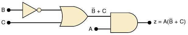
9 4-3 Algebraic Simplification Simplifed logic circuit. z = A(C + B)
10 4-4 Designing Combinational Logic Circuits To solve any logic design problem: Interpret the problem and set up its truth table. Write the AND (product) term for each case where output = 1. Combine the terms in SOP form. Simplify the output expression if possible. Implement the circuit for the final, simplified expression. Circuit that produces a 1 output only for the A = 0, B = 1 condition.

11 4-4 Designing Combinational Logic Circuits An AND gate with appropriate inputs can be used to produce a HIGH output for a specific set of input levels.

12 4-4 Designing Combinational Logic Circuits Each set of input conditions that is to produce a 1 output is implemented by a separate AND gate. The AND outputs are ORed to produce the final output.
13 4-4 Designing Combinational Logic Circuits Truth table for a 3-input circuit. AND terms for each case where output is 1.
14 4-4 Designing Combinational Logic Circuits Design a logic circuit with three inputs, A, B, and C. Output to be HIGH only when a majority inputs are HIGH. Truth table. AND terms for each case where output is 1. SOP expression for the output:

15 4-4 Designing Combinational Logic Circuits Design a logic circuit with three inputs, A, B, and C. Output to be HIGH only when a majority inputs are HIGH. Simplified output expression: Implementing the circuit after factoring: Since the expression is in SOP form, the circuit is a group of AND gates, working into a single OR gate,
16 4-5 Karnaugh Map Method A graphical method of simplifying logic equations or truth tables also called a K map. Theoretically can be used for any number of input variables practically limited to 5 or 6 variables. The truth table values are placed in the K map. Shown here is a two-variable map.
17 4-5 Karnaugh Map Method Four-variable K-Map. Adjacent K map square differ in only one variable both horizontally and vertically. A SOP expression can be obtained by ORing all squares that contain a 1.


 Groups of")
18 4-5 Karnaugh Map Method Looping 1s in adjacent groups of 2, 4, or 8 will result in further simplification. Looping groups of 2 (Pairs) Groups of 4 (Quads) Groups of 8 (Octets)
19 4-5 Karnaugh Map Method When the largest possible groups have been looped, only the common terms are placed in the final expression. Looping may also be wrapped between top, bottom, and sides.
20 4-5 Karnaugh Map Method Complete K map simplification process: Construct the K map, place 1s as indicated in the truth table. Loop 1s that are not adjacent to any other 1s. Loop 1s that are in pairs. Loop 1s in octets even if they have already been looped. Loop quads that have one or more 1s not already looped. Loop any pairs necessary to include 1s not already looped. Form the OR sum of terms generated by each loop. When a variable appears in both complemented and uncomplemented form within a loop, that variable is eliminated from the expression. Variables that are the same for all squares of the loop must appear in the final expression.

21 4-6 Exclusive OR and Exclusive NOR Circuits The exclusive OR (XOR) produces a HIGH output whenever the two inputs are at opposite levels.
22 4-6 Exclusive OR and Exclusive NOR Circuits Exclusive OR circuit and truth table. Output expression: x = AB + AB This circuit produces a HIGH output whenever the two inputs are at opposite levels.
23 4-6 Exclusive OR and Exclusive NOR Circuits Traditional XOR gate symbol. An XOR gate has only two inputs, combined so that x = AB + AB. A shorthand way indicate the XOR output expression is: x = A B. where the symbol represents the XOR gate operation. Output is HIGH only when the two inputs are at different levels. Quad XOR chips containing four XOR gates. 74LS86 Quad XOR (TTL family) 74C86 Quad XOR (CMOS family) 74HC86 Quad XOR (high-speed CMOS)
24 4-6 Exclusive OR and Exclusive NOR Circuits The exclusive NOR (XNOR) produces a HIGH output whenever the two inputs are at the same level. XOR and XNOR outputs are opposite.


25 4-6 Exclusive OR and Exclusive NOR Circuits Exclusive NOR circuit and truth table. Output expression: x = AB + AB XNOR produces a HIGH output whenever the two inputs are at the same levels.
26 4-6 Exclusive OR and Exclusive NOR Circuits Traditional XNOR gate symbol. An XNOR gate has only two inputs, combined so that x = AB + AB. A shorthand way indicate the XOR output expression is: x = A B. XNOR represents inverse of the XOR operation. Output is HIGH only when the two inputs are at the same level. Quad XNOR chips with four XNOR gates. 74LS266 Quad XNOR (TTL family) 74C266 Quad XOR (CMOS) 74HC266 Quad XOR (high-speed CMOS)
27 4-6 Exclusive OR and Exclusive NOR Circuits Truth table and circuit for detecting equality of two-bit binary numbers.


28 4-6 Exclusive OR and Exclusive NOR Circuits How an XNOR gate may be used to simplify circuit implementation.


29 4-7 Parity Generator and Checker XOR and XNOR gates are useful in circuits for parity generation and checking.
30 4-8 Enable/Disable Circuits Situations requiring enable/disable circuits occur frequently in digital circuit design. A circuit is enabled when it allows the passage of an input signal to the output. A circuit is disabled when it prevents the passage of an input signal to the output.
31 4-8 Enable/Disable Circuits

32 4-8 Enable/Disable Circuits A logic circuit that will allow a signal to pass to output only when control inputs B and C are both HIGH. Otherwise, output will stay LOW.
33 4-8 Enable/Disable Circuits A logic circuit that will allow a signal to pass to output only when one, but not both control inputs are HIGH. Otherwise, output will stay HIGH.
34 4-8 Enable/Disable Circuits A logic circuit with input signal A, control input B, and outputs X and Y, which operates as: When B = 1, output X will follow input A, and output Y will be 0. When B = 0, output X will be 0, and output Y will follow input A.

35 4-9 Basic Characteristics of Digital ICs IC chips consist of resistors, diodes & transistors fabricated on a piece of semiconductor material called a substrate. Digital ICs are often categorized by complexity, according to the number of logic gates on the substrate.

36 4-9 Basic Characteristics of Digital ICs The dual-in-line package (DIP) contains two parallel rows of pins. The DIP is probably the most common digital IC package found in older digital equipment.

37 4-9 Basic Characteristics of Digital ICs Pins are numbered counterclockwise, viewed from the top of the package, with respect to an identifying notch or dot at one end. Shown is a 14-pin DIP that measures.75 x.25.

38 4-9 Basic Characteristics of Digital ICs The actual silicon chip is much smaller than the DIP typically about 0.05 square. The silicon chip is connected to the pins of the DIP by very fine (1- mil) wires.

39 4-9 Basic Characteristics of Digital ICs The PLCC is one of many packages common in modern digital circuits. This type uses J-shaped leads which curl under the IC.
40 4-9 Basic Characteristics of Digital ICs ICs are also categorized by the type of components used in their circuits. Bipolar ICs use NPN and PNP transistors Unipolar ICs use FET transistors.

41 4-9 Basic Characteristics of Digital ICs The transistor-transistor logic (TTL) family consists of subfamilies shown here: Differences between the TTL devices is limited to electrical characteristics such as power dissipation & switching speed. Pin layout and logic operations are the same.
42 4-9 Basic Characteristics of Digital ICs V CC for TTL devices is normally +5 V. Power (V CC ) and ground connections are required for chip operation. TTL INVERTER

43 4-9 Basic Characteristics of Digital ICs The Complimentary Metal-Oxide Semiconductor (CMOS) family consists of several series CMOS devices perform the same function as, but are not necessarily pin for pin compatible with TTL devices.
44 4-9 Basic Characteristics of Digital ICs V DD for CMOS devices can be from +3 to +18 V. Power (V DD ) and ground connections are required for chip operation. CMOS INVERTER
45 4-9 Basic Characteristics of Digital ICs Inputs not connected are said to be floating. Floating TTL input acts like a logic 1. Voltage measurement may appear indeterminate, but the device behaves as if there is a 1 on the floating input Floating CMOS inputs can cause overheating and damage to the device. Some ICs have protection circuits built in. The best practice is to tie all unused inputs. Either high or low.

46 4-9 Basic Characteristics of Digital ICs Voltages in the indeterminate range provide unpredictable results and should be avoided. Logic levels for TTL and CMOS devices.
47 4-9 Basic Characteristics of Digital ICs A connection diagram shows all electrical connections, pin numbers, IC numbers, component values, signal names, and power supply voltages. This circuit uses logic gates from two different ICs. Each gate input & output pin number is indicated on the diagram, to easily reference any point in the circuit. Power/ ground connections to each IC are shown.
48 4-9 Basic Characteristics of Digital ICs Logic diagram using Quartus II schematic capture.
49 4-10 Troubleshooting Digital Systems Three basic steps in fixing a digital circuit or system that has a fault (failure): Fault detection determine operation to expected operation. Fault isolation test & measure to isolate the fault. Fault correction repair the fault. The basic troubleshooting tools are the logic probe, oscilloscope, and logic pulser.

50 4-10 Troubleshooting Digital Systems The logic probe will indicate the presence or absence of a signal when touched to a pin as indicated below.
51 4-11 Internal Digital IC Faults Most common internal failures: Malfunction in the internal circuitry. Outputs do not respond properly to inputs. Outputs are unpredictable. Inputs or outputs shorted to ground or V CC. The input will be stuck in LOW or HIGH state. Inputs or outputs open-circuited. An open output will result in a floating indication. Floating input in a TTL will result in a HIGH output. Floating input in a CMOS device will result in erratic or possibly destructive output. Short between two pins (other than ground or V CC ). The signal at those pins will always be identical.
52 4-11 Internal Digital IC Faults These two types of failures force the input signal at the shorted pin to stay in the same state. Left IC input internally shorted to ground. Right IC input internally shorted to supply voltage.
53 4-11 Internal Digital IC Faults These two types of failures do not affect signals at the IC inputs. Left IC output internally shorted to ground. Right IC output internally shorted to supply voltage.
54 4-11 Internal Digital IC Faults An IC with an internally open input will not respond to signals applied to that input pin. An internally open output will produce an unpredictable voltage at that output pin.
55 4-11 Internal Digital IC Faults An internal short between two pins of an IC will force the logic signals at those pins always to be identical. When two input pins are internally shorted, the signals driving these pins are forced to be identical, and usually a signal with three distinct levels results.
56 4-12 External Faults Open signal lines signal prevented from moving between points can be caused by: Broken wire. Poor connections (solder or wire-wrap). Cut or crack on PC board trace. Bent or broken IC pins. Faulty IC socket. This type of fault can be detected visually and verified with an ohmmeter between the points in question.

57 4-12 External Faults What is the most probable fault in the circuit shown? The indeterminate level at the NOR gate output is probably due to the indeterminate input at pin 2. Because there is a LOW at Z1-6, this LOW should also be at Z2-2.
58 4-12 External Faults Shorted signal lines the same signal appears on two or more pins and V CC or ground may also be shorted, caused by: Sloppy wiring. Solder bridges. Incomplete etching. This type of fault can be detected visually and verified with an ohmmeter between the points in question.
59 4-12 External Faults Faulty power supply ICs will not operate or will operate erratically. May lose regulation due to an internal fault or because circuits are drawing too much current. Verify that power supplies provide the specified range of voltages and are properly grounded. Use an oscilloscope to verify that AC ripple is not present and verify that DC voltages stay regulated. Some ICs are more tolerant of power variations and may operate properly others do not. Check power and ground levels at each IC that appears to be operating incorrectly.
60 4-12 External Faults Output loading caused by connecting too many inputs to the output of an IC, exceeding output current rating. Output voltage falls into the indeterminate range. Called loading the output signal. Usually a result of poor design or bad connection.
61 4-14 Programmable Logic Devices The concept behind programmable logic devices is simple lots of logic gates in a single IC. Control of the interconnection of these gates electronically. PLDs allow the design process to be automated. Designers identify inputs, outputs, and logical relationships. PLDs are electronically configured to form the defined logic circuits.
62 4-14 Programmable Logic Devices PLDs use a switch matrix that is often referred to as a programmable array. By deciding which intersections are connected & which are not, we can program the way the inputs are connected to the outputs of the array.

63 4-14 Programmable Logic Devices For out-of-system programming the PLD is placed in a programmer, connected to a PC. PC software translates and loads the information.
64 4-14 Programmable Logic Devices In-system programming is done by connecting directly to portal pins while the IC remains in the system. An interface cable connects the PLD to a PC running the software that loads the device.
65 4-14 Programmable Logic Devices Logic circuits can be described using schematic diagrams, logic equations, truth tables, and HDL. PLD development software can convert any of these descriptions into 1s and 0s and loaded into the PLD. Altera MAX+PLUS II is a development software that allows the user to describe circuits using graphic design files and timing diagrams.

66 4-14 Programmable Logic Devices Hierarchical design small logic circuits are defined and combined with other circuits to form a large section of a project. Large sections can be combined and connected for form a system. Combining blocks developed using different description methods.

67 4-14 Programmable Logic Devices Top-down design requires the definition of subsections that will make up the system. And definition of the individual circuits that will make up each sub section. Each level can be designed and tested individually.

68 4-14 Programmable Logic Devices Timing simulation of a circuit described in HDL.

69 4-14 Programmable Logic Devices A system is built from the bottom up. Each block is described by a design file. After testing it is compiled using development software. The compiled block is tested using a simulator for verify correct operation. A PLD is programmed to verify correct operation.

70 4-15 Representing Data in HDL Every programming language & HDL has its own unique way of identifying number systems. Generally done with a prefix to indicate the system. When we read one of these number designations, we must think of it as a symbol that represents a binary bit pattern. These numeric values are referred to as scalars or literals.
71 4-15 Representing Data in HDL In order to describe a port with more than one data bit we assign a name and the number of bits. This is called a bit array or bit vector. Each element (bit) has a unique index number (0 7) to describe position in the overall structure. HDLs & computer programming languages use this notation.
72 4-15 Representing Data in HDL AHDL Syntax AHDL syntax a name for the bit vector is followed by the range of index designations. Inside square brackets, in the SUBDESIGN section. To declare an eight-bit input port called p1 p1[7..0] :INPUT; --define an 8-bit input port
73 4-15 Representing Data in HDL AHDL Syntax Intermediate variables can be declared as an array of bits. Eight-bit temperature port p1 assigned to a node named temp VARIABLE temp[7..0] :NODE; BEGIN temp[] = p1[] END; The empty braces mean that all bits in the array are being connected. Individual bits could be connected by specifying the bits inside the braces.
74 4-15 Representing Data in HDL VHDL Syntax VHDL syntax a name for the bit vector is followed by the mode, the type, and the range. Enclosed in parenthesis, in the ENTITY section. To declare an eight-bit input port called p1 PORT (p1 :IN BIT_VECTOR (7 DOWNTO 0);
75 4-15 Representing Data in HDL VHDL Syntax Intermediate variables can be declared as an array of bits in the ARCHITECTURE section Eight-bit temperature port p1 assigned to a signal named temp SIGNAL temp :BIT_VECTOR {7 DOWNTO 0}; BEGIN temp <= p1; END; When no elements in the bit vector are specified, all bits in the array are being connected. Individual bits could be connected by specifying bit numbers inside the parentheses.

76 4-15 Representing Data in HDL VHDL offers some standardized data types in libraries collections of VHDL code that can be used to avoid reinventing the wheel. Many convenient functions such as standard TTL device descriptions are contained in macrofunctions.

77 4-16 Truth Tables Using HDL - AHDL Circuits can be designed directly from truth tables, using AHDL and VHDL.


78 4-16 Truth Tables Using HDL - VHDL Circuits can be designed directly from truth tables, using AHDL and VHDL.

79 4-17 Decision Control Structures in HDL IF/THEN/ELSE IF/THEN/ELSE statements provide a framework for making logical decisions in a system IF/THEN is used when there is a choice between doing something and doing nothing.

80 4-17 Decision Control Structures in HDL IF/THEN/ELSE IF/THEN/ELSE statements provide a framework for making logical decisions in a system IF/THEN/ELSE is used when there is a choice of two possible actions.

81 4-17 Decision Control Structures in HDL IF/THEN/ELSE IF/THEN/ELSE in AHDL:

82 4-17 Decision Control Structures in HDL IF/THEN/ELSE IF/THEN/ELSE in VHDL:

83 4-17 Decision Control Structures in HDL ELSIF By combining IF and ELSE decisions, we can create a control structure referred to as ELSIF Which chooses one of many possible outcomes. As each condition is evaluated, it performs an action if true or goes on to evaluate the next condition.


84 4-17 Decision Control Structures in HDL ELSIF A temperature measuring system using an A/D converter. IF the digital value is less than or equal to 8 THEN light only the Too Cold indicator. ELSE IF the digital value is greater than 8 AND less than 11 THEN light only the Just Right indicator. ELSE light only the Too Hot indicator.

85 4-17 Decision Control Structures in HDL ELSIF ELSIF in AHDL:

86 4-17 Decision Control Structures in HDL ELSIF ELSIF in VHDL:
87 4-17 Decision Control Structures in HDL - CASE The CASE construct determines the value of an expression or object. Then goes through a list of values (cases) to determine what action to take. Different than the IF/ELSEIF, as there is only one action or match for a case statement.

88 4-17 Decision Control Structures in HDL - CASE CASE construct in AHDL:

89 4-17 Decision Control Structures in HDL - CASE CASE construct in VHDL:


90 4-17 Decision Control Structures in HDL - CASE A vending machine coin detector accepts quarters, dimes & nickels, activating the corresponding digital signal (Q, D, N) only when the correct coin is present. A digital circuit must use the Q, D, and N, signals as inputs and produce a binary number that represents the value of the coin

91 4-17 Decision Control Structures in HDL - CASE The coin detector in AHDL:

92 4-17 Decision Control Structures in HDL - CASE The coin detector in VHDL:
93 END
Chapter 4 Combinational Logic Circuits
 Chapter 4 Combinational Logic Circuits Chapter 4 Objectives Selected areas covered in this chapter: Converting logic expressions to sum-of-products expressions. Boolean algebra and the Karnaugh map as
Lecture 15 Analysis of Combinational Circuits
 Lecture 15 Analysis of Combinational Circuits Designing Combinational Logic Circuits A logic circuit having 3 inputs, A, B, C will have its output HIGH only when a majority of the inputs are HIGH. Step
Chapter 3 Describing Logic Circuits Dr. Xu
 Chapter 3 Describing Logic Circuits Dr. Xu Chapter 3 Objectives Selected areas covered in this chapter: Operation of truth tables for AND, NAND, OR, and NOR gates, and the NOT (INVERTER) circuit. Boolean
DELD UNIT 3. Question Option A Option B Option C Option D Correct Option A B C
 Class : S.E.Comp Matoshri College of Engineering and Research Center Nasik Department of Computer Engineering Digital Elecronics and Logic Design (DELD) UNIT - III Subject : DELD Sr. No. Question Option
CHAPTER 3 BASIC & COMBINATIONAL LOGIC CIRCUIT
 CHAPTER 3 BASIC & COMBINATIONAL LOGIC CIRCUIT CHAPTER CONTENTS 3.1 Introduction to Basic Gates 3.2 Analysing A Combinational Logic Circuit 3.3 Design A Combinational Logic Circuit From Boolean Expression
Subject: Analog and Digital Electronics Code:15CS32
 Subject: Analog and Digital Electronics Code:15CS32 Syllabus: The Basic Gates : Review of Basic Logic gates, Positive and Negative Logic, Introduction to HDL. Combinational Logic Circuits:Sum-of-Products
Name: Class: Date: 1. As more electronic systems have been designed using digital technology, devices have become smaller and less powerful.
 Name: Class: Date: DE Midterm Review 2 True/False Indicate whether the statement is true or false. 1. As more electronic systems have been designed using digital technology, devices have become smaller
Gates and Circuits 1
 1 Gates and Circuits Chapter Goals Identify the basic gates and describe the behavior of each Describe how gates are implemented using transistors Combine basic gates into circuits Describe the behavior
Odd-Prime Number Detector The table of minterms is represented. Table 13.1
 Odd-Prime Number Detector The table of minterms is represented. Table 13.1 Minterm A B C D E 1 0 0 0 0 1 3 0 0 0 1 1 5 0 0 1 0 1 7 0 0 1 1 1 11 0 1 0 1 1 13 0 1 1 0 1 17 1 0 0 0 1 19 1 0 0 1 1 23 1 0 1
Function Table of an Odd-Parity Generator Circuit
 Implementation of an Odd-Parity Generator Circuit The first step in implementing any circuit is to represent its operation in terms of a Truth or Function table. The function table for an 8-bit data as
Chapter 1: Digital logic
 Chapter 1: Digital logic I. Overview In PHYS 252, you learned the essentials of circuit analysis, including the concepts of impedance, amplification, feedback and frequency analysis. Most of the circuits
ECE380 Digital Logic
 ECE38 Digital Logic Optimized Implementation of Logic Functions: Karnaugh Maps and Minimum Sum-of-Product Forms Dr. D. J. Jackson Lecture 7- Karnaugh map The key to finding a minimum cost SOP or POS form
Lecture 7: Digital Logic
 Lecture 7: Digital Logic Last time we introduced the concept of digital electronics i.e., one identifies a range of voltages with the value, and another range with the value But we didn t specify these
Logic Design I (17.341) Fall Lecture Outline
 Fall Lecture Outline") Logic Design I (17.341) Fall 2011 Lecture Outline Class # 07 October 31, 2011 / November 07, 2011 Dohn Bowden 1 Today s Lecture Administrative Main Logic Topic Homework 2 Course Admin 3 Administrative
Logic Design I (17.341) Fall 2011 Lecture Outline Class # 07 October 31, 2011 / November 07, 2011 Dohn Bowden 1 Today s Lecture Administrative Main Logic Topic Homework 2 Course Admin 3 Administrative
BOOLEAN ALGEBRA AND LOGIC FAMILIES
 C H A P T E R 7 Learning Objectives Unique Feature of Boolean Algebra Laws of Boolean Algebra Equivalent Switching Circuits DeMorgan s Theorem s The Sum-of-Products (SOP) Form The Standard SOP Form The
University of Technology
 University of Technology Lecturer: Dr. Sinan Majid Course Title: microprocessors 4 th year Lecture 7 & 8 NAND and XOR Implementations Combinational Design Procedure NAND-NAND & NOR-NOR Networks DeMorgan
2 Logic Gates THE INVERTER. A logic gate is an electronic circuit which makes logic decisions. It has one output and one or more inputs.
 2 Logic Gates A logic gate is an electronic circuit which makes logic decisions. It has one output and one or more inputs. THE INVERTER The inverter (NOT circuit) performs the operation called inversion
Digital Fundamentals. Lab 4 EX-OR Circuits & Combinational Circuit Design
 Richland College School of Engineering & Technology Rev. 0 B. Donham Rev. 1 (7/2003) J. Horne Rev. 2 (1/2008) J. Bradbury Digital Fundamentals CETT 1425 Lab 4 EX-OR Circuits & Combinational Circuit Design
Number system: the system used to count discrete units is called number. Decimal system: the number system that contains 10 distinguished
 Number system: the system used to count discrete units is called number system Decimal system: the number system that contains 10 distinguished symbols that is 0-9 or digits is called decimal system. As
ECE380 Digital Logic
 ECE380 Digital Logic Implementation Technology: Standard Chips and Programmable Logic Devices Dr. D. J. Jackson Lecture 10-1 Standard chips A number of chips, each with a few logic gates, are commonly
Digital Fundamentals 8/29/2016. Summary. Summary. Floyd. Chapter 3 A X. The Inverter
 Digital Fundamentals Tenth Edition Floyd Chapter 3 The Inverter The inverter performs the oolean NOT operation. When the input is LOW, the output is HIGH; when the input is HIGH, the output is LOW. Input
Chapter 2 Introduction to Logic Circuits
 Chapter 2 Introduction to Logic Circuits Logic unctions and circuits Boolean algebra Snthesis o digital circuits Introduction to CAD tools Introduction to VHDL Logic unctions and Circuits and 2 are binar
Gates and and Circuits
 Chapter 4 Gates and Circuits Chapter Goals Identify the basic gates and describe the behavior of each Describe how gates are implemented using transistors Combine basic gates into circuits Describe the
Digital Fundamentals 9/4/2017. Summary. Summary. Floyd. Chapter 3. The Inverter
 Digital Fundamentals Tenth Edition Floyd Chapter 3 29 Pearson Education, Upper 28 Pearson Saddle River, Education NJ 7458. ll Rights Reserved The Inverter The inverter performs the oolean NOT operation.
CS302 Digital Logic Design Solved Objective Midterm Papers For Preparation of Midterm Exam
 CS302 Digital Logic Design Solved Objective Midterm Papers For Preparation of Midterm Exam MIDTERM EXAMINATION 2011 (October-November) Q-21 Draw function table of a half adder circuit? (2) Answer: - Page
Logic diagram: a graphical representation of a circuit
 LOGIC AND GATES Introduction to Logic (1) Logic diagram: a graphical representation of a circuit Each type of gate is represented by a specific graphical symbol Truth table: defines the function of a gate
Digital Fundamentals
 Digital Fundamentals Tenth Edition Floyd hapter 5 Floyd, Digital Fundamentals, th ed 28 Pearson Education 29 Pearson Education, Upper Saddle River, NJ 7458. ll Rights Reserved ombinational Logic ircuits
Lecture 2: Digital Logic Basis
 Lecture 2: Digital Logic Basis Xufeng Kou School of Information Science and Technology ShanghaiTech University 1 Outline Truth Table Basic Logic Operation and Gates Logic Circuits NOR Gates and NAND Gates
Combinational Circuits: Multiplexers, Decoders, Programmable Logic Devices
 Combinational Circuits: Multiplexers, Decoders, Programmable Logic Devices Lecture 5 Doru Todinca Textbook This chapter is based on the book [RothKinney]: Charles H. Roth, Larry L. Kinney, Fundamentals
CS302 - Digital Logic Design Glossary By
 CS302 - Digital Logic Design Glossary By ABEL : Advanced Boolean Expression Language; a software compiler language for SPLD programming; a type of hardware description language (HDL) Adder : A digital
4-bit counter circa bit counter circa 1990
 Digital Logic 4-bit counter circa 1960 8-bit counter circa 1990 Logic gates Operates on logical values (TRUE = 1, FALSE = 0) NOT AND OR XOR 0-1 1-0 0 0 0 1 0 0 0 1 0 1 1 1 0 0 0 1 0 1 0 1 1 1 1 1 0 0 0
Associate In Applied Science In Electronics Engineering Technology Expiration Date:
 PROGRESS RECORD Study your lessons in the order listed below. Associate In Applied Science In Electronics Engineering Technology Expiration Date: 1 2330A Current and Voltage 2 2330B Controlling Current
Digital Electronics Course Objectives
 Digital Electronics Course Objectives In this course, we learning is reported using Standards Referenced Reporting (SRR). SRR seeks to provide students with grades that are consistent, are accurate, and
(CSC-3501) Lecture 6 (31 Jan 2008) Seung-Jong Park (Jay) CSC S.J. Park. Announcement
 Lecture 6 (31 Jan 2008) Seung-Jong Park (Jay) CSC S.J. Park. Announcement") Seung-Jong Park (Jay) http://www.csc.lsu.edu/~sjpark Computer Architecture (CSC-3501) Lecture 6 (31 Jan 2008) 1 Announcement 2 1 Reminder A logic circuit is composed of: Inputs Outputs Functional specification
Seung-Jong Park (Jay) http://www.csc.lsu.edu/~sjpark Computer Architecture (CSC-3501) Lecture 6 (31 Jan 2008) 1 Announcement 2 1 Reminder A logic circuit is composed of: Inputs Outputs Functional specification
DO NOT COPY DO NOT COPY
 18 Chapter 1 Introduction 1.9 Printed-Circuit oards printed-circuit board n IC is normally mounted on a printed-circuit board (PC) [or printed-wiring (PC) board (PW)] that connects it to other ICs in a
Logic Symbols with Truth Tables INVERTER A B NAND A B C NOR C A B A B C XNOR A B C A B Digital Logic 1
 Slide Logic Symbols with Truth Tables UFFER INVERTER ND NND OR NOR XOR XNOR 6.7 Digital Logic Digital logic can be described in terms of standard logic symbols and their corresponding truth tables. The
COMPUTER ORGANIZATION & ARCHITECTURE DIGITAL LOGIC CSCD211- DEPARTMENT OF COMPUTER SCIENCE, UNIVERSITY OF GHANA
 COMPUTER ORGANIZATION & ARCHITECTURE DIGITAL LOGIC LOGIC Logic is a branch of math that tries to look at problems in terms of being either true or false. It will use a set of statements to derive new true
Department of EECS. University of California, Berkeley. Logic gates. September 1 st 2001
 Department of EECS University of California, Berkeley Logic gates Bharathwaj Muthuswamy and W. G. Oldham September 1 st 2001 1. Introduction This lab introduces digital logic. You use commercially available
Digital Fundamentals
 Digital Fundamentals Tenth Edition Floyd Chapter 3 28 Pearson Education 29 Pearson Education, Upper Saddle River, NJ 7458. ll Rights Reserved The Inverter The inverter performs the oolean NOT operation.
Logic Circuit Design
 Logic Circuit Design we have studied Truth Tables Logic gates Logic algebra K-maps 1 All these are tools Tools Truth Tables Logic gates Logic algebra K-maps 2 All these are tools Tools Truth Tables Logic
EXPERIMENT 12: DIGITAL LOGIC CIRCUITS
 EXPERIMENT 12: DIGITAL LOGIC CIRCUITS The purpose of this experiment is to gain some experience in the use of digital logic circuits. These circuits are used extensively in computers and all types of electronic
Objective Questions. (a) Light (b) Temperature (c) Sound (d) all of these
 Light (b) Temperature (c) Sound (d) all of these") Objective Questions Module 1: Introduction 1. Which of the following is an analog quantity? (a) Light (b) Temperature (c) Sound (d) all of these 2. Which of the following is a digital quantity? (a) Electrical
Objective Questions Module 1: Introduction 1. Which of the following is an analog quantity? (a) Light (b) Temperature (c) Sound (d) all of these 2. Which of the following is a digital quantity? (a) Electrical
Chapter 3 Digital Logic Structures
 Chapter 3 Digital Logic Structures Transistor: Building Block of Computers Microprocessors contain millions of transistors Intel Pentium 4 (2): 48 million IBM PowerPC 75FX (22): 38 million IBM/Apple PowerPC
Philips Semiconductors Programmable Logic Devices
 DESCRIPTION The PLD is a high speed, combinatorial Programmable Logic Array. The Philips Semiconductors state-of-the-art Oxide Isolated Bipolar fabrication process is employed to produce maximum propagation
Module-1: Logic Families Characteristics and Types. Table of Content
 1 Module-1: Logic Families Characteristics and Types Table of Content 1.1 Introduction 1.2 Logic families 1.3 Positive and Negative logic 1.4 Types of logic families 1.5 Characteristics of logic families
Digital Logic Circuits
 Digital Logic Circuits Let s look at the essential features of digital logic circuits, which are at the heart of digital computers. Learning Objectives Understand the concepts of analog and digital signals
UNIT-2: BOOLEAN EXPRESSIONS AND COMBINATIONAL LOGIC CIRCUITS
 UNIT-2: BOOLEAN EXPRESSIONS AND COMBINATIONAL LOGIC CIRCUITS STRUCTURE 2. Objectives 2. Introduction 2.2 Simplification of Boolean Expressions 2.2. Sum of Products 2.2.2 Product of Sums 2.2.3 Canonical
Digital Fundamentals. Logic gates
 Digital Fundamentals Logic gates Objectives Describe the operation of the inverter, the AND gate, and the OR gate Describe the operation of the NAND gate and the NOR gate Express the operation of the NOT,
6.1 In this section, you will design (but NOT build) a circuit with 4 inputs,
 a circuit with 4 inputs,") EE 2449 Experiment 6 Jack Levine and Nancy Warter-Perez //208 CALIFORNIA STATE UNIVERSITY LOS ANGELES Department of Electrical and Computer Engineering EE-2449 Digital Logic Lab EXPERIMENT 6 COMBINATIONAL
EE 2449 Experiment 6 Jack Levine and Nancy Warter-Perez //208 CALIFORNIA STATE UNIVERSITY LOS ANGELES Department of Electrical and Computer Engineering EE-2449 Digital Logic Lab EXPERIMENT 6 COMBINATIONAL
Asst. Prof. Thavatchai Tayjasanant, PhD. Power System Research Lab 12 th Floor, Building 4 Tel: (02)
") 2145230 Aircraft Electricity and Electronics Asst. Prof. Thavatchai Tayjasanant, PhD Email: taytaycu@gmail.com aycu@g a co Power System Research Lab 12 th Floor, Building 4 Tel: (02) 218-6527 1 Chapter
2145230 Aircraft Electricity and Electronics Asst. Prof. Thavatchai Tayjasanant, PhD Email: taytaycu@gmail.com aycu@g a co Power System Research Lab 12 th Floor, Building 4 Tel: (02) 218-6527 1 Chapter
Course Overview. Course Overview
 Course Overview Where does this course fit into the Electrical Engineering curriculum? Page 5 Course Overview Where does this course fit into the Computer Engineering curriculum? Page 6 3 Course Content
Digital Electronics. A. I can list five basic safety rules for electronics. B. I can properly display large and small numbers in proper notation,
 St. Michael Albertville High School Teacher: Scott Danielson September 2016 Content Skills Learning Targets Standards Assessment Resources & Technology CEQ: WHAT MAKES DIGITAL ELECTRONICS SO IMPORTANT
Unit 1 Foundations in Electronics - Lesson 1.1 Introduction to Electronics Standards Essential Question Enduring Understandings
 Course: DIGITAL ELECTRONICS- PROJECT LEAD THE WAY (DE-PLTW) Year: 2017-2018 Teacher: Mr. Christopher Reynolds/ Mr. Kenneth Rice Unit 1 Foundations in Electronics - Lesson 1.1 Introduction to Electronics
PREVIEW COPY. Digital Logic Systems. Table of Contents. Digital Logic Fundamentals...3. Logic Building Blocks Medium- and Large-Scale ICs...
 Digital Logic Systems Table of Contents Lesson One Lesson Two Lesson Three Digital Logic Fundamentals...3 Logic uilding locks...9 Medium- and Large-Scale ICs...35 Lesson Four Functional Logic Systems...5
4-bit counter circa bit counter circa 1990
 Digital Logic 4-bit counter circa 1960 8-bit counter circa 1990 Logic gates Operates on logical values (TRUE = 1, FALSE = 0) NOT AND OR XOR 0-1 1-0 0 0 0 1 0 0 0 1 0 1 1 1 0 0 0 1 0 1 0 1 1 1 1 1 0 0 0
MODULE-4 Memory and programmable logic
 MODULE-4 Memory and programmable logic READ-ONLY MEMORY (ROM) A read-only memory (ROM) is a device that includes both the decoder and the OR gates within a single IC package. The connections between the
Module-3: Metal Oxide Semiconductor (MOS) & Emitter coupled logic (ECL) families
 & Emitter coupled logic (ECL) families") 1 Module-3: Metal Oxide Semiconductor (MOS) & Emitter coupled logic (ECL) families 1. Introduction 2. Metal Oxide Semiconductor (MOS) logic 2.1. Enhancement and depletion mode 2.2. NMOS and PMOS inverter
1 Module-3: Metal Oxide Semiconductor (MOS) & Emitter coupled logic (ECL) families 1. Introduction 2. Metal Oxide Semiconductor (MOS) logic 2.1. Enhancement and depletion mode 2.2. NMOS and PMOS inverter
Multiple Category Scope and Sequence: Scope and Sequence Report For Course Standards and Objectives, Content, Skills, Vocabulary
 Multiple Category Scope and Sequence: Scope and Sequence Report For Course Standards and Objectives, Content, Skills, Vocabulary Wednesday, August 20, 2014, 1:16PM Unit Course Standards and Objectives
Basic Characteristics of Digital ICs
 ECEN202 Section 2 Characteristics of Digital IC s Part 1: Specification of characteristics An introductory look at digital IC s: Logic families Basic construction and operation Operating characteristics
Digital Circuits II Lecture 6. Lab Demonstration 3 Using Altera Quartus II to Determine Simplified Equations & Entering Truth Table into VHDL
 Digital Circuits II Lecture 6 Lab Demonstration 3 Using Altera Quartus II to Determine Simplified Equations & Entering Truth Table into VHDL References (Text Book): 1) Digital Electronics, 9 th editon,
R & D Electronics DIGITAL IC TRAINER. Model : DE-150. Feature: Object: Specification:
 DIGITAL IC TRAINER Model : DE-150 Object: To Study the Operation of Digital Logic ICs TTL and CMOS. To Study the All Gates, Flip-Flops, Counters etc. To Study the both the basic and advance digital electronics
B.C.A 2017 DIGITAL ELECTRONICS BCA104T MODULE SPECIFICATION SHEET. Course Outline
 Course Outline B.C.A 2017 DIGITAL ELECTRONICS BCA104T MODULE SPECIFICATION SHEET The purpose of the course is to teach principles of digital electronics. This course covers varieties of topics including
QUIZ. What do these bits represent?
 QUIZ What do these bits represent? 1001 0110 1 QUIZ What do these bits represent? Unsigned integer: 1101 1110 Signed integer (2 s complement): Fraction: IBM 437 character: Latin-1 character: Huffman-compressed
Module 4: Design and Analysis of Combinational Circuits 1. Module-4. Design and Analysis of Combinational Circuits
 1 Module-4 Design and Analysis of Combinational Circuits 4.1 Motivation: This topic develops the fundamental understanding and design of adder, substractor, code converter multiplexer, demultiplexer etc
Digital Systems Principles and Applications TWELFTH EDITION. 3-3 OR Operation With OR Gates. 3-4 AND Operations with AND gates
 Digital Systems Principles and Applications TWELFTH EDITION CHAPTER 3 Describing Logic Circuits Part -2 J. Bernardini 3-3 OR Operation With OR Gates An OR gate is a circuit with two or more inputs, whose
Exercise 1: AND/NAND Logic Functions
 Exercise 1: AND/NAND Logic Functions EXERCISE OBJECTIVE When you have completed this exercise, you will be able to determine the operation of an AND and a NAND logic gate. You will verify your results
Introduction to CMOS VLSI Design (E158) Lecture 5: Logic
 Lecture 5: Logic") Harris Introduction to CMOS VLSI Design (E158) Lecture 5: Logic David Harris Harvey Mudd College David_Harris@hmc.edu Based on EE271 developed by Mark Horowitz, Stanford University MAH E158 Lecture 5 1
Harris Introduction to CMOS VLSI Design (E158) Lecture 5: Logic David Harris Harvey Mudd College David_Harris@hmc.edu Based on EE271 developed by Mark Horowitz, Stanford University MAH E158 Lecture 5 1
SYNTHESIS OF COMBINATIONAL CIRCUITS
 HPTER 6 SYNTHESIS O OMINTIONL IRUITS 6.1 Introduction oolean functions can be expressed in the forms of sum-of-products and productof-sums. These expressions can also be minimized using algebraic manipulations
Classification of Digital Circuits
 Classification of Digital Circuits Combinational logic circuits. Output depends only on present input. Sequential circuits. Output depends on present input and present state of the circuit. Combinational
EEE 301 Digital Electronics
 EEE 301 Digital Electronics Lecture 1 Course Contents Introduction to number systems and codes. Analysis and synthesis of digital logic circuits: Basic logic functions, Boolean algebra,combinational logic
Lab Project #2: Small-Scale Integration Logic Circuits
 Lab Project #2: Small-Scale Integration Logic Circuits Duration: 2 weeks Weeks of 1/31/05 2/7/05 1 Objectives The objectives of this laboratory project are to design some simple logic circuits using small-scale
Propagation Delay, Circuit Timing & Adder Design. ECE 152A Winter 2012
 Propagation Delay, Circuit Timing & Adder Design ECE 152A Winter 2012 Reading Assignment Brown and Vranesic 2 Introduction to Logic Circuits 2.9 Introduction to CAD Tools 2.9.1 Design Entry 2.9.2 Synthesis
Propagation Delay, Circuit Timing & Adder Design
 Propagation Delay, Circuit Timing & Adder Design ECE 152A Winter 2012 Reading Assignment Brown and Vranesic 2 Introduction to Logic Circuits 2.9 Introduction to CAD Tools 2.9.1 Design Entry 2.9.2 Synthesis
Entry Level Assessment Blueprint Electronics Technology
 Blueprint Test Code: 4135 / Version: 01 Specific Competencies and Skills Tested in this Assessment: Safety Practices Demonstrate safe working procedures Explain the purpose of OSHA and how it promotes
Chapter 4 Logic Functions and Gates
 Chapter 4 Logic Functions and Gates CHPTER OJECTIVES Upon successful completion of this chapter, you will be able to: Describe the basic logic functions: ND, OR, and NOT. Draw simple switch circuits to
Code No: R Set No. 1
 Code No: R05310402 Set No. 1 1. (a) What are the parameters that are necessary to define the electrical characteristics of CMOS circuits? Mention the typical values of a CMOS NAND gate. (b) Design a CMOS
Digital Electronics 8. Multiplexer & Demultiplexer
 1 Module -8 Multiplexers and Demultiplexers 1 Introduction 2 Principles of Multiplexing and Demultiplexing 3 Multiplexer 3.1 Types of multiplexer 3.2 A 2 to 1 multiplexer 3.3 A 4 to 1 multiplexer 3.4 Multiplex
Number of Lessons:155 #14B (P) Electronics Technology with Digital and Microprocessor Laboratory Completion Time: 42 months
 Electronics Technology with Digital and Microprocessor Laboratory Completion Time: 42 months") PROGRESS RECORD Study your lessons in the order listed below. Number of Lessons:155 #14B (P) Electronics Technology with Digital and Microprocessor Laboratory Completion Time: 42 months 1 2330A Current
PROGRESS RECORD Study your lessons in the order listed below. Number of Lessons:155 #14B (P) Electronics Technology with Digital and Microprocessor Laboratory Completion Time: 42 months 1 2330A Current
Exercise 2: OR/NOR Logic Functions
 Exercise 2: OR/NOR Logic Functions EXERCISE OBJECTIVE When you have completed this exercise, you will be able to determine the operation of an OR and a NOR logic gate. You will verify your results by generating
Multiple input gates. The AND gate
 Multiple input gates Inverters and buffers exhaust the possibilities for single-input gate circuits. What more can be done with a single logic signal but to buffer it or invert it? To explore more logic
Positive and Negative Logic
 Course: B.Sc. Applied Physical Science (Computer Science) Year & Sem.: IInd Year, Sem - IIIrd Subject: Computer Science Paper No.: IX Paper Title: Computer System Architecture Lecture No.: 4 Lecture Title:
Digital Electronic Concepts
 Western Technical College 10662137 Digital Electronic Concepts Course Outcome Summary Course Information Description Career Cluster Instructional Level Total Credits 4.00 Total Hours 108.00 This course
Physics 335 Lab 1 Intro to Digital Logic
 Physics 33 Lab 1 Intro to Digital Logic We ll be introducing you to digital logic this quarter. Some things will be easier for you than analog, some things more difficult. Digital is an all together different
Fault Tolerance in VLSI Systems
 Fault Tolerance in VLSI Systems Overview Opportunities presented by VLSI Problems presented by VLSI Redundancy techniques in VLSI design environment Duplication with complementary logic Self-checking logic
EMT1250 LABORATORY EXPERIMENT. EXPERIMENT # 4: Combinational Logic Circuits. Name: Date:
 EXPERIMENT # 4: Combinational Logic Circuits Name: Date: Equipment/Parts Needed: 5V DC Power Supply Digital Trainer (Logic Probe) Breadboard DIP Switch 7400 NAND gate 7402 NOR gate 7404 Inverter 7408 AND
In this lecture: Lecture 8: ROM & Programmable Logic Devices
 In this lecture: Lecture 8: ROM Programmable Logic Devices Dr Pete Sedcole Department of EE Engineering Imperial College London http://caseeicacuk/~nps/ (Floyd, 3 5, 3) (Tocci 2, 24, 25, 27, 28, 3 34)
ELEC 350L Electronics I Laboratory Fall 2012
 ELEC 350L Electronics I Laboratory Fall 2012 Lab #9: NMOS and CMOS Inverter Circuits Introduction The inverter, or NOT gate, is the fundamental building block of most digital devices. The circuits used
UNIT-IV Combinational Logic
 UNIT-IV Combinational Logic Introduction: The signals are usually represented by discrete bands of analog levels in digital electronic circuits or digital electronics instead of continuous ranges represented
Subtractor Logic Schematic
 Function Of Xor Gate In Parallel Adder Subtractor Logic Schematic metic functions, including half adder, half subtractor, full adder, independent logic gates to form desired circuits based on dif- by integrating
User s Manual ISL70040SEHEV2Z. User s Manual: Evaluation Board. High Reliability
 User s Manual ISL70040SEHEV2Z User s Manual: Evaluation Board High Reliability Rev 0.00 Nov 2017 USER S MANUAL ISL70040SEHEV2Z Evaluation Board for the ISL70040SEH and ISL70023SEH UG147 Rev.0.00 1. Overview
PHYSICAL STRUCTURE OF CMOS INTEGRATED CIRCUITS. Dr. Mohammed M. Farag
 PHYSICAL STRUCTURE OF CMOS INTEGRATED CIRCUITS Dr. Mohammed M. Farag Outline Integrated Circuit Layers MOSFETs CMOS Layers Designing FET Arrays EE 432 VLSI Modeling and Design 2 Integrated Circuit Layers
Digital Fundamentals A Systems Approach Thomas L. Floyd First Edition
 Digital Fundamentals Systems pproach Thomas L. Floyd First Edition Pearson Education Limited Edinburgh Gate Harlow Essex M20 2JE England and ssociated ompanies throughout the world Visit us on the World
Exercise 1: EXCLUSIVE OR/NOR Gate Functions
 EXCLUSIVE-OR/NOR Gates Digital Logic Fundamentals Exercise 1: EXCLUSIVE OR/NOR Gate Functions EXERCISE OBJECTIVE When you have completed this exercise, you will be able to demonstrate the operation of
Careers in Electronics Using a Calculator Safety Precautions Dc Circuits p. 1 Fundamentals of Electricity p. 3 Matter, Elements, and Compounds p.
 Preface p. vii Careers in Electronics p. xii Using a Calculator p. xvi Safety Precautions p. xix Dc Circuits p. 1 Fundamentals of Electricity p. 3 Matter, Elements, and Compounds p. 4 A Closer Look at
ECE 172 Digital Systems. Chapter 2 Digital Hardware. Herbert G. Mayer, PSU Status 6/30/2018
 ECE 172 Digital Systems Chapter 2 Digital Hardware Herbert G. Mayer, PSU Status 6/30/2018 1 Syllabus l Term Sharing l Standard Forms l Hazards l Decoders l PLA vs. PAL l PROM l Bibliography 2 Product Term
Use the fixed 5 volt supplies for your power in digital circuits, rather than the variable outputs.
 Physics 33 Lab 1 Intro to Digital Logic We ll be introducing you to digital logic this quarter. Some things will be easier for you than analog, some things more difficult. Digital is an all together different
Combinational Logic Circuits. Combinational Logic
 Combinational Logic Circuits The outputs of Combinational Logic Circuits are only determined by the logical function of their current input state, logic 0 or logic 1, at any given instant in time. The
Digital Systems Design
 Digital Systems Design Digital Systems Design and Test Dr. D. J. Jackson Lecture 1-1 Introduction Traditional digital design Manual process of designing and capturing circuits Schematic entry System-level
Lab# 13: Introduction to the Digital Logic
 Lab# 13: Introduction to the Digital Logic Revision: October 30, 2007 Print Name: Section: In this lab you will become familiar with Physical and Logical Truth tables. As well as asserted high, asserted
In this lecture: Lecture 3: Basic Logic Gates & Boolean Expressions
 In this lecture: Lecture 3: Basic Logic Gates & Boolean Expressions Dr Pete Sedcole Department of E&E Engineering Imperial College London http://cas.ee.ic.ac.uk/~nps/ (Floyd 3.1 3.6, 4.1) (Tocci 3.1 3.9)