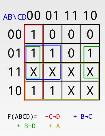
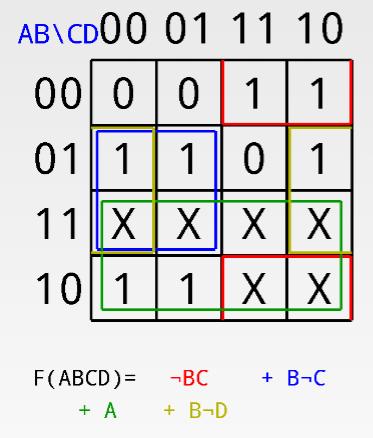
UNIT-IV Combinational Logic
|
|
|
- Cory Richards
- 5 years ago
- Views:
Transcription
1 UNIT-IV Combinational Logic Introduction: The signals are usually represented by discrete bands of analog levels in digital electronic circuits or digital electronics instead of continuous ranges represented in analogue electronics. The simple electronic representations of Boolean logic functions, large assemblies of logic gates are typically used to make digital electronic circuits. In digital circuit theory, the circuits, thus formed from logic gates are used to generate outputs based on the input logic. Hence, these circuits are called as logic circuits and are classified into two types such as sequential logic and combinational logic circuits. The logic gates can be defined as simple physical devices used to implement the Boolean function. Logic gates are used to perform a logical operation with one or more inputs and generates a logical output. These logic circuits are formed by connecting one or more logic gates together. These logic circuits are classified into two types: sequential logic circuits and combinational logic circuits. Combinational Logic Circuit Definition The combinational logic circuits or time-independent logic circuits in digital circuit theory can be defined as a type of digital logic circuit implemented using Boolean circuits, where the output of logic circuit is a pure function of the present inputs only. The combinational logic circuit operation is instantaneous and these circuits do not have the memory or feedback loops. This combinational logic is in contrast compared to the sequential logic circuit in which the output depends on both present inputs and also on the previous inputs. Thus, we can say that combinational logic does not have memory, whereas sequential logic stores previous input in its memory. Hence, if the input of combinational logic circuit changes, then the output also changes.

2 Classification of Combinational Logic The combinational logic circuits can be classified into various types based on the purpose of usage, such as arithmetic & logical functions, data transmission, and code converters. To solve the arithmetic and logical functions we generally use adders, subtractors, and comparators which are generally realized by combining various logic gates called as combinational logic circuits. Similarly, for data transmission, we use multiplexers, demultiplexers, encoders, and decoders which are also realized using combinational logic. The code converters such as binary, BCD, and 7-segment are designed using various logic circuits. ANALYSIS OF COMBINATIONAL LOGIC FUNCTIONS There are 3 ways to represent combinational logic functions. Logic gates - Logic gates are used as the building blocks in the design of combinational logic circuits. These gates are the AND, OR, NOT, NAND, NOR gates. 2. Boolean Algebra - Boolean Algebra specifies the relationship between Boolean variables which is used to design digital circuits using Logic Gates. Every logic circuit can be completely described using the Boolean operations, because the OR, AND gate, and NOT gates are the basic building blocks of digital systems. 3. Truth table - A truth table is used in logic to compute the functional values of logical expressions on each combination of values taken by their logical variables. If a combination logic block have more than one bit output, each single-bit output gets its own truth-table. Often they are combined into a single table with multiple output columns, one for each single-bit output. Design procedure The design procedure for combinational logic circuits starts with the problem specification and comprises the following steps:
3 Determine required number of inputs and outputs from the specifications. Derive the truth table for each of the outputs based on their relationships to the input. Simplify the boolean expression for each output. Use Karnaugh Maps or Boolean algebra. Draw a logic diagram that represents the simplified Boolean expression. Verify the design by analysing or simulating the circuit. EAMPLE: Is input greater than or equal to 5? Specification Design a circuit that has a 3-bit binary input and a single output (Z) specified as follows: Z =, when the input is less than 5 Z =, otherwise. Determine the inputs and Outputs. Label the inputs (3 bits) as A, B, C A is the most significant bit C is the least significant bit 2. The output ( bit) is Z Z = -> 2, 2, 2 Z = -> other inputs 2. Derive the Truth Table Truth Table A B C Z
4 3. Simplify the Boolean Expression From the truth table, we use one of the following 2 methods to obtain the simplified boolean expression o o Use Karnaugh Map to minimise the logic or From the truth table, get the Canonical Sum of Products boolean expression. Z = A * ~B * C + A * B * ~C + A * B * C Use Boolean Algebra to simplify the boolean expression to: Z = (B + C) * A 4. Draw the logic diagram Draw a logic diagram that represents the simplified Boolean expression. Verify the design by analysing or simulating the circuit. Bool Expression Z = (B + C) * A Truth Table A B C Z A Half Adder Circuit A half adder is a logical circuit that performs an addition operation on two binary digits. The half adder produces a sum and a carry value which are both binary digits. Half Adder Truth Table with Carry-Out Symbol Truth Table B A SUM CARRY


5 From the truth table of the half adder we can see that the SUM (S) output is the result of the Exclusive-OR gate and the Carry-out (Cout) is the result of the AND gate. Then the Boolean expression for a half adder is as follows. For the SUM bit: SUM = A OR B = A B For the CARRY bit: CARRY = A AND B = A.B One major disadvantage of the Half Adder circuit when used as a binary adder, is that there is no provision for a Carry-in from the previous circuit when adding together multiple data bits. Full Adder Truth Table with Carry Symbol Truth Table C-in B A Sum Cout
6 Then the Boolean expression for a full adder is as follows. For the SUM (S) bit: SUM = (A OR B) OR Cin = (A B) Cin For the CARRY-OUT (Cout) bit: CARRY-OUT = A AND B OR Cin(A OR B) = A.B + Cin(A B) An n-bit Binary Adder We have seen above that single -bit binary adders can be constructed from basic logic gates. But what if we wanted to add together two n-bit numbers, then n number of -bit full adders need to be connected or cascaded together to produce what is known as a Ripple Carry Adder. A ripple carry adder is simply n, -bit full adders cascaded together with each full adder representing a single weighted column in a long binary addition. It is called a ripple carry adder because the carry signals produce a ripple effect through the binary adder from right to left, (LSB to MSB). For example, suppose we want to add together two 4-bit numbers, the two outputs of the first full adder will provide the first place digit sum (S) of the addition plus a carry-out bit that acts as the carry-in digit of the next binary adder. The second binary adder in the chain also produces a summed output (the 2nd bit) plus another carry-out bit and we can keep adding more full adders to the combination to add larger numbers, linking the carry bit output from the first full binary adder to the next full adder, and so forth. An example of a 4-bit adder is given below.


7 A 4-bit Ripple Adder A Half Subtractor Circuit A half subtractor is a logical circuit that performs a subtraction operation on two binary digits. The half subtractor produces a sum and a borrow bit for the next stage. Half Subtractor with Borrow-out Symbol Truth Table Y DIFFERENCE BORROW
8 From the truth table of the half subtractor we can see that the DIFFERENCE ( D) output is the result of the Exclusive-OR gate and the Borrow-out (Bout) is the result of the NOT-AND combination. Then the Boolean expression for a half subtractor is as follows. For the DIFFERENCE bit: D = OR Y = Y For the BORROW bit B = not- AND Y =.Y If we compare the Boolean expressions of the half subtractor with a half adder, we can see that the two expressions for the SUM (adder) and DIFFERENCE (subtractor) are exactly the same and so they should be because of the Exclusive-OR gate function. The two Boolean expressions for the binary subtractor BORROW is also very similar to that for the adders CARRY. Then all that is needed to convert a half adder to a half subtractor is the inversion of the minuend input. One major disadvantage of the Half Subtractor circuit when used as a binary subtractor, is that there is no provision for a Borrow-in from the previous circuit when subtracting multiple data bits from each other. Then we need to produce what is called a full binary subtractor circuit to take into account this borrow-in input from a previous circuit. A Full Binary Subtractor Circuit The main difference between the Full Subtractor and the previous Half Subtractor circuit is that a full subtractor has three inputs. The two single bit data inputs (minuend) and Y (subtrahend) the same as before plus an additional Borrow-in (B-in) input to receive the borrow generated by the subtraction process from a previous stage as shown below. Full Subtractor Block Diagram Then the combinational circuit of a full subtractor performs the operation of subtraction on three binary bits producing outputs for the difference Dand borrow Bout. Just like the binary adder circuit, the full subtractor can also be thought of as two half subtractors connected together, with the first half subtractor passing its borrow to the second half subtractor as follows.


9 Full Subtractor Logic Diagram As the full subtractor circuit above represents two half subtractors cascaded together, the truth table for the full subtractor will have eight different input combinations as there are three input variables, the data bits and the Borrow-in, BIN input. Also includes the difference output, D and the Borrow-out, BOUT bit. Full Subtractor Truth Table Symbol Truth Table Bin Y Diff. B-out Then the Boolean expression for a full subtractor is as follows. For the DIFFERENCE (D) bit:
BIN An n-bit Binary Subtractor As with the binary adder, we can also have n number of -bit full binary subtractor connected or cascaded together to subtract two parallel n-bitnumbers from")
, the process of subtraction becomes an addition as we can use two s complement notation on all the bits in the subtrahend and setting")
10 D = (.Y.BIN) + (.Y.BIN) + (.Y.BIN) + (.Y.BIN) which can be simplified too: D = ( OR Y) OR BIN = ( Y) BIN For the BORROW OUT (BOUT) bit: BOUT = (.Y.BIN) + (.Y.BIN) + (.Y.BIN) + (.Y.BIN) which will also simplify too: BOUT = AND Y OR ( OR Y)BIN =.Y + ( Y)BIN An n-bit Binary Subtractor As with the binary adder, we can also have n number of -bit full binary subtractor connected or cascaded together to subtract two parallel n-bitnumbers from each other. For example two 4-bit binary numbers. We said before that the only difference between a full adder and a full subtractor was the inversion of one of the inputs. So by using an n-bit adder and n number of inverters (NOT Gates), the process of subtraction becomes an addition as we can use two s complement notation on all the bits in the subtrahend and setting the carry input of the least significant bit to a logic (HIGH). Binary Subtractor using 2 s Complement

11 COMPARATOR -bit Digital Comparator Circuit Then the operation of a -bit digital comparator is given in the following Truth Table. Digital Comparator Truth Table Inputs Outputs B A A>B A=B A<B You may notice two distinct features about the comparator from the above truth table. Firstly, the circuit does not distinguish between either two or two s as an output A = B is produced when they are both equal, either A = B = or A = B =. Secondly, the output condition for A = B resembles that of a commonly available logic gate, the ExclusiveNOR or Ex-NOR function (equivalence) on each of the nbits giving: Q = A B


 are compared to each other to produce the relevant output with one word connected to inputs A and the other")
12 Digital comparators actually use Exclusive-NOR gates within their design for comparing their respective pairs of bits. When we are comparing two binary or BCD values or variables against each other, we are comparing the magnitude of these values, a logic against a logic which is where the term Magnitude Comparator comes from. As well as comparing individual bits, we can design larger bit comparators by cascading together n of these and produce a n-bit comparator just as we did for the n-bit adder in the previous tutorial. Multi-bit comparators can be constructed to compare whole binary or BCD words to produce an output if one word is larger, equal to or less than the other. A very good example of this is the 4-bit Magnitude Comparator. Here, two 4-bit words ( nibbles ) are compared to each other to produce the relevant output with one word connected to inputs A and the other to be compared against connected to input B as shown below. 4-bit Magnitude Comparator Binary Decoder Binary Decoder is another combinational logic circuit constructed from individual logic gates and is the exact opposite to that of an Encoder

13 This simple example above of a 2-to-4 line binary decoder consists of an array of four AND gates. The 2 binary inputs labelled A and B are decoded into one of 4 outputs, hence the description of 2-to-4 binary decoder. Each output represents one of the miniterms of the 2 input variables, (each output = a miniterm). The binary inputs A and B determine which output line from Q to Q3 is HIGH at logic level while the remaining outputs are held LOW at logic so only one output can be active (HIGH) at any one time. Therefore, whichever output line is HIGH identifies the binary code present at the input, in other words it de-codes the binary input. Some binary decoders have an additional input pin labelled Enable that controls the outputs from the device. This extra input allows the decoders outputs to be turned ON or OFF as required. These types of binary decoders are commonly used as memory address decoders in microprocessor memory applications. We have seen that a 2-to-4 line binary decoder (TTL 7455) can be used for decoding any 2-bit binary code to provide four outputs, one for each possible input combination. However, sometimes it is required to have a Binary Decoder with a number of outputs greater than is available, so by adding more inputs, the decoder can potentially provide 2n more outputs. So for example, a decoder with 3 binary inputs ( n = 3 ), would produce a 3-to-8 line decoder (TTL 7438) and 4 inputs ( n = 4 ) would produce a 4-to-6 line decoder (TTL 7454) and so on. But a decoder can also have less than 2 noutputs such as the BCD to seven-segment decoder (TTL 7447) which has 4 inputs and only 7 active outputs to drive a display rather than the full 6 (24) outputs as you would expect. Here a much larger 4 (3 data plus enable) to 6 line binary decoder has been implemented using two smaller 3-to-8 decoders.


14 A 4-to-6 Binary Decoder Configuration Inputs A, B, C are used to select which output on either decoder will be at logic (HIGH) and input D is used with the enable input to select which encoder either the first or second will output the. Encoder Encoders take all of their data inputs one at a time and converts them into an equivalent binary code at its output Unlike a multiplexer that selects one individual data input line and then sends that data to a single output line or switch, Digital Encoder more commonly called a Binary Encoder takes ALL its data inputs one at a time and then converts them into a single encoded output. So we can say that a binary encoder, is a multi-input combinational logic circuit that converts the logic level data at its inputs into an equivalent binary code at its output.
15 Generally, digital encoders produce outputs of 2-bit, 3-bit or 4-bit codes depending upon the number of data input lines. An n-bit binary encoder has 2n input lines and n-bit output lines with common types that include 4-to-2, 8-to-3 and 6-to-4 line configurations. The output lines of a digital encoder generate the binary equivalent of the input line whose value is equal to and are available to encode either a decimal or hexadecimal input pattern to typically a binary or B.C.D (binary coded decimal) output code. 4-to-2 Bit Binary Encoder One of the main disadvantages of standard digital encoders is that they can generate the wrong output code when there is more than one input present at logic level. For example, if we make inputs D and D2 HIGH at logic both at the same time, the resulting output is neither at or at but will be at which is an output binary number that is different to the actual input present. Also, an output code of all logic s can be generated when all of its inputs are at OR when input D is equal to one. One simple way to overcome this problem is to Prioritise the level of each input pin. So if there is more than one input at logic level at the same time, the actual output code would only correspond to the input with the highest designated priority. Then this type of digital encoder is known commonly as a Priority Encoder or Pencoder for short. Priority Encoder The Priority Encoder solves the problems mentioned above by allocating a priority level to each input. The priority encoders output corresponds to the currently active input which has the highest priority. So when an input with a higher priority is present, all other inputs with a lower priority will be ignored. It's applications includes used to control interrupt requests by acting on the highest priority request
 inputs and provides a 3-bit")
 as this has the highest order out")
16 to encode the output of a flash analog to digital converter The priority encoder comes in many different forms with an example of an 8-input priority encoder along with its truth table shown below. 8-to-3 Bit Priority Encoder Priority encoders are available in standard IC form and the TTL 74LS48 is an 8-to-3 bit priority encoder which has eight active LOW (logic ) inputs and provides a 3-bit code of the highest ranked input at its output. Priority encoders output the highest order input first for example, if input lines D2, D3 and D5 are applied simultaneously the output code would be for input D5 ( ) as this has the highest order out of the 3 inputs. Once input D5 had been removed the next highest output code would be for input D3 ( ), and so on. The truth table for a 8-to-3 bit priority encoder is given as: Digital Inputs Binary Output D7 D6 D5 D4 D3 D2 D D Q2 Q Q


17 Where equals dont care, that is logic or a logic. From this truth table, the Boolean expression for the encoder above with data inputs D to D7 and outputs Q, Q, Q2 is given as: Output Q Output Q Output Q2

 the lower priority bits are shown as don't cares ().")
18 Then the final Boolean expression for the priority encoder including the zero inputs is defined as: Priority Encoder Output Expression In practice these zero inputs would be ignored allowing the implementation of the final Boolean expression for the outputs of the 8-to-3 priority encoder. We can constructed a simple encoder from the expression above using individual OR gates as follows. Digital Encoder using Logic Gates 4 to 2 priority encoder A 4-to-2 priority encoder takes 4 input bits and produces 2 output bits. In this truth table, for all the non-explicitly defined input combinations (i.e. inputs containing 2, 3, or 4 high bits) the lower priority bits are shown as don't cares (). Similarly when the inputs are, the outputs are not valid and therefore they are. Truth Table I3 I2 I I O O
19 From the above truth table, we can obtain the full truth table required for our design. Truth Table I3 I2 I I O O

20 From this truth table, we use the Karnaugh Map to minimise the logic to the following boolean expressions: O = I2 + I3 O = ~I2 * I + I3 Implementation of the 4 to 2 priority encoder using combinational logic circuits. The Multiplexer The multiplexer is a combinational logic circuit designed to switch one of several input lines to a single common output line Multiplexing is the generic term used to describe the operation of sending one or more analogue or digital signals over a common transmission line at different times or speeds and as such, the device we use to do just that is called a Multiplexer. The multiplexer, shortened to MU or MP, is a combinational logic circuit designed to switch one of several input lines through to a single common output line by the application of a control signal. Multiplexers operate like very


21 fast acting multiple position rotary switches connecting or controlling multiple input lines called channels one at a time to the output. Multiplexers, or MU s, can be either digital circuits made from high speed logic gates used to switch digital or binary data or they can be analogue types using transistors, MOSFET s or relays to switch one of the voltage or current inputs through to a single output. The most basic type of multiplexer device is that of a one-way rotary switch as shown. Basic Multiplexing Switch Generally, the selection of each input line in a multiplexer is controlled by an additional set of inputs called control lines and according to the binary condition of these control inputs, either HIGH or LOW the appropriate data input is connected directly to the output. Normally, a multiplexer has an even number of 2n data input lines and a number of control inputs that correspond with the number of data inputs. Note that multiplexers are different in operation to Encoders. Encoders are able to switch an n-bit input pattern to multiple output lines that represent the binary coded (BCD) output equivalent of the active input.


22 4 Channel Multiplexer using logic gates The Demultiplexer The demultiplexer is a combinational logic circuit designed to switch one common input line to one of several seperate output line The data distributor, known more commonly as a Demultiplexer or Demux for short, is the exact opposite of the Multiplexer we saw in the previous tutorial. The demultiplexer takes one single input data line and then switches it to any one of a number of individual output lines one at a time. The demultiplexerconverts a serial data signal at the input to a parallel data at its output lines as shown below. -to-4 Channel De-multiplexer

23 S S A B C D F O O O O F O O O O F O O O O F The Boolean expression for this -to-4 Demultiplexer above with outputs Ato D and data select lines a, b is given as: F= The function of the Demultiplexer is to switch one common data input line to any one of the 4 output data lines A to D in our example above. As with the multiplexer the individual solid state switches are selected by the binary input address code on the output select pins a and b as shown. Demultiplexer Output Line Selection As with the previous multiplexer circuit, adding more address line inputs it is possible to switch more outputs giving a -to-2n data line outputs. Some standard demultiplexer IC s also have an additional enable output pin which disables or prevents the input from being passed to the selected output. Also some have latches built into their outputs to maintain the output logic level after the address inputs have been changed. However, in standard decoder type circuits the address input will determine which single data output will have the same value as the data input with all other data outputs having the value of logic.


24 The implementation of the Boolean expression above using individual logic gates would require the use of six individual gates consisting of AND and NOT gates as shown. 4 Channel Demultiplexer using Logic Gates. CODE CONVERTERS Converting Binary to Gray Code B3 B2 B B G3 G2 G G
25 Converting Gray to Binary Code G3 G2 G G B3 B2 B B
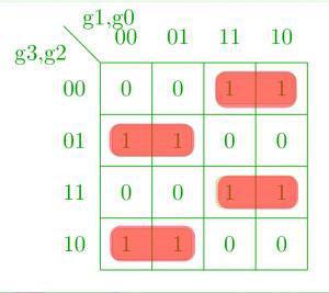
26 Converting BCD(842) to Excess-3 A B C D W Y Z
 W Y Z A B C D")
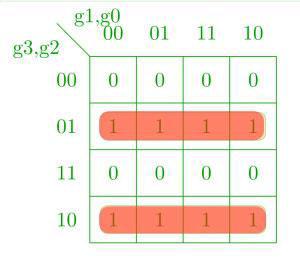
27 Converting Excess-3 to BCD(842) W Y Z A B C D

28 BCD TO 7-SEGMENT DECODER

29 CIRCUIT DIAGRAM
30 Binary Multiplier Circuit Let us consider two unsigned 2 bit binary numbers A and B to generalize the multiplication process. The multiplicand A is equal to AA and the multiplier B is equal to BB. The figure below shows the multiplication process of two 2 bit binary numbers. This process involves the multiplication of two digits and the addition of digits with or without carry. After the multiplication of the each bit to the multiplicand, partial products are generated, and then these products are added to produce the total sum which represents the binary multiplication value. This multiplication is implemented by combinational circuit such that the multiplication is performed with AND gates whereas the addition is carried out
31 by using half adders as shown in figure. The first partial product is obtained by the AND gate which is nothing but a least significant bit of the multiplication result. Since the second partial product is shifted to the left position, the first partial second term and second partial product first term is added by half adder and produce the sum output along with the carry out. This carry out is added at the next half adder as an input as shown in figure. Likewise, it produces the multiplication result of two binary numbers by using the simple circuit configuration. The multiplication of the two 2 bit number results a 4-bit binary number. Let us consider two unsigned 4 bit numbers multiplication in which the multiplicand, A is equal to A3A2 AA and the multiplier B is equal to B3B2BB. The partial products are produced depending on each multiplier bit multiplied by the multiplicand. Each partial product consists of four product terms and these are shifted to the left relative to the previous partial product as shown in figure. All these partial products are added to produce the 8 bit product.
32 The logic circuit for the 4 4 binary multiplication can be implemented by using three binary full adders along with AND gates. In the above operation the first partial product is obtained by multiplying B with A3A2 AA, the second partial product is formed by multiplying B with A3A2 AA, likewise for 3rd and 4th partial products. So these partial products can be implemented with AND gates as shown in figure. These partial products are then added by using 4 bit parallel adder. The three most significant bits of first partial product with carry (considered as zero) are added with second partial term in the first full adder. Then the result is added to the next partial product with carry out and it goes on till the final partial product, finally it produces 8 bit sum which indicates the multiplication value of the two binary numbers.
33 Decimal Adder / BCD Adder: Decimal Adder The digital systems handles the decimal number in the form of binary coded decimal numbers (BCD). A BCD adder is a circuit that adds two BCD digits and produces a sum digit also in BCD. BCD numbers use digits, to 9 which are represented in the binary form to, i.e. each BCD digit is represented as a 4-bit binary number. When we write BCD number say 526, it can be represented as Here, we should note that BCD cannot be greater than 9. The addition of two BCD numbers can be best understood by considering the three cases that occur when two BCD digits are added. Sum Equals 9 or less with carry Let us consider additions of 3 and 6 in BCD.
34 The addition is carried out as in normal binary addition and the sum is, which is BCD code for 9. Sum greater than 9 with carry The sum is an invalid BCD number. This has occurred because the sum of the two digits exceeds 9. Whenever this occurs the sum has to be corrected by the addition of six () in the invalid BCD number, as shown below After addition of 6 carry is produced into the second decimal position. Sum equals 9 or less with carry Let us consider addition of 8 and 9 in BCD
35 In this, case, result ( ) is valid BCD number, but it is incorrect. To get the correct BCD result correction factor of 6 has to be added to the least significant digit sum, as shown below Going through these three cases of BCD addition we can summarise the BCD addition procedure as follows :. Add two BCD numbers using ordina7 binary addition. 2. If four-bit sum is equal to or less than 9, no correction is needed. The sum is in proper BCD form. 3. If the four-bit sum is greater than 9 or if a carry is generated from the four-bit sum, the sum is invalid. 4. To correct the invalid sum, add 2 to the four-bit sum. If a carry results from this addition, add it to the next higher-order BCD digit. 5. Thus to implement BCD adder we require : 6. 4-bit binary adder for initial addition 7. Logic circuit to detect sum greater than 9 and 8. One more 4-bit adder to add 2 in the sum if sum is greater than 9 or carry is. The logic circuit to detect sum greater than 9 can be determined by simplifying the boolean expression of given truth table.
36 With this design information we can draw the block diagram of BCD adder, as shown in the Fig As shown in the Fig. 3.32, the two BCD numbers, together with input carry, are first added in the top 4-bit binary adder to produce a binary sum. When the output carry is equal to zero (i.e. when sum 9 and Cout = ) nothing (zero) is added to the binary sum. When it is equal to one (i.e. when sum > 9 or Cout = ), binary is added to the binary sum through the bottom 4-bit binary adder. The output carry generated from the bottom binary adder can be ignored, since it supplies information already available at the output-carry terminal.
Combinational Logic Circuits. Combinational Logic
 Combinational Logic Circuits The outputs of Combinational Logic Circuits are only determined by the logical function of their current input state, logic 0 or logic 1, at any given instant in time. The
COMBINATIONAL CIRCUIT
 Combinational circuit is a circuit in which we combine the different gates in the circuit, for example encoder, decoder, multiplexer and demultiplexer. Some of the characteristics of combinational circuits
Module 4: Design and Analysis of Combinational Circuits 1. Module-4. Design and Analysis of Combinational Circuits
 1 Module-4 Design and Analysis of Combinational Circuits 4.1 Motivation: This topic develops the fundamental understanding and design of adder, substractor, code converter multiplexer, demultiplexer etc
16 Multiplexers and De-multiplexers using gates and ICs. (74150, 74154)
") 16 Multiplexers and De-multiplexers using gates and ICs. (74150, 74154) Aim: To design multiplexers and De-multiplexers using gates and ICs. (74150, 74154) Components required: Digital IC Trainer kit,
16 Multiplexers and De-multiplexers using gates and ICs. (74150, 74154) Aim: To design multiplexers and De-multiplexers using gates and ICs. (74150, 74154) Components required: Digital IC Trainer kit,
EXPERIMENT NO 1 TRUTH TABLE (1)
") EPERIMENT NO AIM: To verify the Demorgan s theorems. APPARATUS REQUIRED: THEORY: Digital logic trainer and Patch cords. The digital signals are discrete in nature and can only assume one of the two values
EPERIMENT NO AIM: To verify the Demorgan s theorems. APPARATUS REQUIRED: THEORY: Digital logic trainer and Patch cords. The digital signals are discrete in nature and can only assume one of the two values
Combinational Circuits DC-IV (Part I) Notes
 Notes") Combinational Circuits DC-IV (Part I) Notes Digital Circuits have been classified as: (a) Combinational Circuits: In these circuits output at any instant of time depends on inputs present at that instant
Combinational Circuits DC-IV (Part I) Notes Digital Circuits have been classified as: (a) Combinational Circuits: In these circuits output at any instant of time depends on inputs present at that instant
DESIGN OF 4 BIT BINARY ARITHMETIC CIRCUIT USING 1 S COMPLEMENT METHOD
 e-issn 2455 1392 Volume 2 Issue 4, April 2016 pp. 176-187 Scientific Journal Impact Factor : 3.468 http://www.ijcter.com DESIGN OF 4 BIT BINARY ARITHMETIC CIRCUIT USING 1 S COMPLEMENT METHOD Dhrubojyoti
Electronics. Digital Electronics
 Electronics Digital Electronics Introduction Unlike a linear, or analogue circuit which contains signals that are constantly changing from one value to another, such as amplitude or frequency, digital
LOGIC DIAGRAM: HALF ADDER TRUTH TABLE: A B CARRY SUM. 2012/ODD/III/ECE/DE/LM Page No. 1
 LOGIC DIAGRAM: HALF ADDER TRUTH TABLE: A B CARRY SUM K-Map for SUM: K-Map for CARRY: SUM = A B + AB CARRY = AB 22/ODD/III/ECE/DE/LM Page No. EXPT NO: DATE : DESIGN OF ADDER AND SUBTRACTOR AIM: To design
Digital Applications (CETT 1415) Credit: 4 semester credit hours (3 hours lecture, 4 hours lab) Prerequisite: CETT 1403 & CETT 1405
 Credit: 4 semester credit hours (3 hours lecture, 4 hours lab) Prerequisite: CETT 1403 & CETT 1405") Digital Applications () Credit: 4 semester credit hours (3 hours lecture, 4 hours lab) Prerequisite: CETT 1403 & CETT 1405 Course Description This course covers digital techniques and numbering systems,
Digital Applications () Credit: 4 semester credit hours (3 hours lecture, 4 hours lab) Prerequisite: CETT 1403 & CETT 1405 Course Description This course covers digital techniques and numbering systems,
4:Combinational logic circuits. 3 July
 4:Combinational logic circuits 3 July 2014 1 overview What is combinational logic circuit? Examples of combinational logic circuits Binary-adder Binary-subtractor Binary-multiplier Decoders Multiplexers
Department of Electronics and Communication Engineering
 Department of Electronics and Communication Engineering Sub Code/Name: BEC3L2- DIGITAL ELECTRONICS LAB Name Reg No Branch Year & Semester : : : : LIST OF EXPERIMENTS Sl No Experiments Page No Study of
LIST OF EXPERIMENTS. KCTCET/ /Odd/3rd/ETE/CSE/LM
 LIST OF EXPERIMENTS. Study of logic gates. 2. Design and implementation of adders and subtractors using logic gates. 3. Design and implementation of code converters using logic gates. 4. Design and implementation
Unit 3. Logic Design
 EE 2: Digital Logic Circuit Design Dr Radwan E Abdel-Aal, COE Logic and Computer Design Fundamentals Unit 3 Chapter Combinational 3 Combinational Logic Logic Design - Introduction to Analysis & Design
BCD Adder. Lecture 21 1
 BCD Adder -BCD adder A 4-bit binary adder that is capable of adding two 4-bit words having a BCD (binary-coded decimal) format. The result of the addition is a BCD-format 4-bit output word, representing
SRV ENGINEERING COLLEGE SEMBODAI RUKMANI VARATHARAJAN ENGINEERING COLLEGE SEMBODAI
 SEMBODAI RUKMANI VARATHARAJAN ENGINEERING COLLEGE SEMBODAI 6489 (Approved By AICTE,Newdelhi Affiliated To ANNA UNIVERSITY::Chennai) CS 62 DIGITAL ELECTRONICS LAB (REGULATION-23) LAB MANUAL DEPARTMENT OF
Gates and Circuits 1
 1 Gates and Circuits Chapter Goals Identify the basic gates and describe the behavior of each Describe how gates are implemented using transistors Combine basic gates into circuits Describe the behavior
UNIT III. Designing Combinatorial Circuits. Adders
 UNIT III Designing Combinatorial Circuits The design of a combinational circuit starts from the verbal outline of the problem and ends with a logic circuit diagram or a set of Boolean functions from which
COMBINATIONAL LOGIC CIRCUIT First Class. Dr. AMMAR ABDUL-HAMED KHADER
 COMBINATIONAL LOGIC CIRCUIT First Class 1 BASIC ADDER Adders are important in computers and also in other types of digital system in which numerical data are processed. An understanding of the basic operation
Digital Electronics 8. Multiplexer & Demultiplexer
 1 Module -8 Multiplexers and Demultiplexers 1 Introduction 2 Principles of Multiplexing and Demultiplexing 3 Multiplexer 3.1 Types of multiplexer 3.2 A 2 to 1 multiplexer 3.3 A 4 to 1 multiplexer 3.4 Multiplex
UNIT-2: BOOLEAN EXPRESSIONS AND COMBINATIONAL LOGIC CIRCUITS
 UNIT-2: BOOLEAN EXPRESSIONS AND COMBINATIONAL LOGIC CIRCUITS STRUCTURE 2. Objectives 2. Introduction 2.2 Simplification of Boolean Expressions 2.2. Sum of Products 2.2.2 Product of Sums 2.2.3 Canonical
Asst. Prof. Thavatchai Tayjasanant, PhD. Power System Research Lab 12 th Floor, Building 4 Tel: (02)
") 2145230 Aircraft Electricity and Electronics Asst. Prof. Thavatchai Tayjasanant, PhD Email: taytaycu@gmail.com aycu@g a co Power System Research Lab 12 th Floor, Building 4 Tel: (02) 218-6527 1 Chapter
2145230 Aircraft Electricity and Electronics Asst. Prof. Thavatchai Tayjasanant, PhD Email: taytaycu@gmail.com aycu@g a co Power System Research Lab 12 th Floor, Building 4 Tel: (02) 218-6527 1 Chapter
TABLE 3-2 Truth Table for Code Converter Example
 997 by Prentice-Hall, Inc. Mano & Kime Upper Saddle River, New Jersey 7458 T-28 TABLE 3-2 Truth Table for Code Converter Example Decimal Digit Input BCD Output Excess-3 A B C D W Y Z 2 3 4 5 6 7 8 9 Truth
Experiment # 4. Binary Addition & Subtraction. Eng. Waleed Y. Mousa
 Experiment # 4 Binary Addition & Subtraction Eng. Waleed Y. Mousa 1. Objectives: 1. To study adder and subtractor circuits using logic gates. 2. To construct and test various adders and subtractor circuits.
Digital Applications (CETT 1415) Credit: 4 semester credit hours (3 hours lecture, 4 hours lab) Prerequisite: CETT 1403 & CETT 1405
 Credit: 4 semester credit hours (3 hours lecture, 4 hours lab) Prerequisite: CETT 1403 & CETT 1405") Digital Applications (CETT 1415) Credit: 4 semester credit hours (3 hours lecture, 4 hours lab) Prerequisite: CETT 1403 & CETT 1405 Course Description This course covers digital techniques and numbering
Digital Applications (CETT 1415) Credit: 4 semester credit hours (3 hours lecture, 4 hours lab) Prerequisite: CETT 1403 & CETT 1405 Course Description This course covers digital techniques and numbering
Digital Electronics. Functions of Combinational Logic
 Digital Electronics Functions of Combinational Logic Half-dder Basic rules of binary addition are performed by a half adder, which has two binary inputs ( and B) and two binary outputs (Carry out and Sum).
Gates and and Circuits
 Chapter 4 Gates and Circuits Chapter Goals Identify the basic gates and describe the behavior of each Describe how gates are implemented using transistors Combine basic gates into circuits Describe the
CS302 Digital Logic Design Solved Objective Midterm Papers For Preparation of Midterm Exam
 CS302 Digital Logic Design Solved Objective Midterm Papers For Preparation of Midterm Exam MIDTERM EXAMINATION 2011 (October-November) Q-21 Draw function table of a half adder circuit? (2) Answer: - Page
Laboratory Manual CS (P) Digital Systems Lab
 Digital Systems Lab") Laboratory Manual CS 09 408 (P) Digital Systems Lab INDEX CYCLE I A. Familiarization of digital ICs and digital IC trainer kit 1 Verification of truth tables B. Study of combinational circuits 2. Verification
Laboratory Manual CS 09 408 (P) Digital Systems Lab INDEX CYCLE I A. Familiarization of digital ICs and digital IC trainer kit 1 Verification of truth tables B. Study of combinational circuits 2. Verification
Number system: the system used to count discrete units is called number. Decimal system: the number system that contains 10 distinguished
 Number system: the system used to count discrete units is called number system Decimal system: the number system that contains 10 distinguished symbols that is 0-9 or digits is called decimal system. As
Combinational Logic. Rab Nawaz Khan Jadoon DCS. Lecturer COMSATS Lahore Pakistan. Department of Computer Science
 Combinational Logic Rab Nawaz Khan Jadoon DCS COMSATS Institute of Information Technology Lecturer COMSATS Lahore Pakistan Digital Logic and Computer Design 2 Combinational logic A combinational circuit
Experiment # 3 Combinational Circuits (I) Binary Addition and Subtraction
 Binary Addition and Subtraction") Experiment # 3 Combinational Circuits (I) Binary Addition and Subtraction Objectives: 1. To study adder and subtractor circuits using logic gates. 2. To construct and test various adders and subtractor
Experiment # 3 Combinational Circuits (I) Binary Addition and Subtraction Objectives: 1. To study adder and subtractor circuits using logic gates. 2. To construct and test various adders and subtractor
2 Building Blocks. There is often the need to compare two binary values.
 2 Building Blocks 2.1 Comparators There is often the need to compare two binary values. This is done using a comparator. A comparator determines whether binary values A and B are: 1. A = B 2. A < B 3.
FUNCTION OF COMBINATIONAL LOGIC CIRCUIT
 HAPTER FUNTION OF OMBINATIONAL LOGI IRUIT OUTLINE HALF-ADDER ANF FULL ADDER IRUIT -BIT PARALLEL BINARY RIPPLE ARRY ADDER -BIT PARALLEL BINARY ARRY LOOK- AHEAD ADDER BD ADDER IRUIT DEODER ENODER MULTIPLEXER
Fan in: The number of inputs of a logic gate can handle.
 Subject Code: 17333 Model Answer Page 1/ 29 Important Instructions to examiners: 1) The answers should be examined by key words and not as word-to-word as given in the model answer scheme. 2) The model
Sr. No. Instrument Specifications. TTL (Transistor-Transistor Logic) based on bipolar junction transistors
 based on bipolar junction transistors") MIT College of Engineering, Pune. Department of Electronics & Telecommunication (Electronics Lab) EXPERIMENT NO 01 TITLE OF THE EXPERIMENT: Verify four voltage and current parameters for TTL and CMOS (IC
MIT College of Engineering, Pune. Department of Electronics & Telecommunication (Electronics Lab) EXPERIMENT NO 01 TITLE OF THE EXPERIMENT: Verify four voltage and current parameters for TTL and CMOS (IC
Function Table of an Odd-Parity Generator Circuit
 Implementation of an Odd-Parity Generator Circuit The first step in implementing any circuit is to represent its operation in terms of a Truth or Function table. The function table for an 8-bit data as
IES Digital Mock Test
 . The circuit given below work as IES Digital Mock Test - 4 Logic A B C x y z (a) Binary to Gray code converter (c) Binary to ECESS- converter (b) Gray code to Binary converter (d) ECESS- To Gray code
CHAPTER 5 DESIGN OF COMBINATIONAL LOGIC CIRCUITS IN QCA
 90 CHAPTER 5 DESIGN OF COMBINATIONAL LOGIC CIRCUITS IN QCA 5.1 INTRODUCTION A combinational circuit consists of logic gates whose outputs at any time are determined directly from the present combination
CHW 261: Logic Design
 CHW 6: Logic Design Instructors: Prof. Hala Zayed Dr. Ahmed Shalaby http://www.bu.edu.eg/staff/halazayed4 http://bu.edu.eg/staff/ahmedshalaby4# Slide Copyright 6 by Pearson Education, Inc. Upper Saddle
Unit level 4 Credit value 15. Introduction. Learning Outcomes
 Unit 20: Unit code Digital Principles T/615/1494 Unit level 4 Credit value 15 Introduction While the broad field of electronics covers many aspects, it is digital electronics which now has the greatest
Logic diagram: a graphical representation of a circuit
 LOGIC AND GATES Introduction to Logic (1) Logic diagram: a graphical representation of a circuit Each type of gate is represented by a specific graphical symbol Truth table: defines the function of a gate
Chapter 1: Digital logic
 Chapter 1: Digital logic I. Overview In PHYS 252, you learned the essentials of circuit analysis, including the concepts of impedance, amplification, feedback and frequency analysis. Most of the circuits
 Class Subject Code Subject Prepared By Lesson Plan for Time: Lesson. No 1.CONTENT LIST: Introduction to UnitII 2. SKILLS ADDRESSED: Learning I year, 02 sem CS6201 Digital Principles & System Design S.Seedhanadevi
CS302 - Digital Logic Design Glossary By
 CS302 - Digital Logic Design Glossary By ABEL : Advanced Boolean Expression Language; a software compiler language for SPLD programming; a type of hardware description language (HDL) Adder : A digital
COMPUTER ARCHITECTURE AND ORGANIZATION
 DEPARTMENT OF COMPUTER SCIENCE AND ENGINEERING COMPUTER ARCHITECTURE AND ORGANIZATION (CSE18R174) LAB MANUAL Name of the Student:..... Register No Class Year/Sem/Class :. :. :... 1 This page is left intentionally
MSI Design Examples. Designing a circuit that adds three 4-bit numbers
 MSI Design Examples In this lesson, you will see some design examples using MSI devices. These examples are: Designing a circuit that adds three 4-bit numbers. Design of a 4-to-16 Decoder using five 2-to-4
MAHALAKSHMI ENGINEERING COLLEGE TIRUCHIRAPALLI
 MAHALAKSHMI ENGINEERING COLLEGE TIRUCHIRAPALLI 6 DEPARTMENT: ECE QUESTION BANK SUBJECT NAME: DIGITAL SYSTEM DESIGN SEMESTER III SUBJECT CODE: EC UNIT : Design of Combinational Circuits PART -A ( Marks).
DELD UNIT 3. Question Option A Option B Option C Option D Correct Option A B C
 Class : S.E.Comp Matoshri College of Engineering and Research Center Nasik Department of Computer Engineering Digital Elecronics and Logic Design (DELD) UNIT - III Subject : DELD Sr. No. Question Option
Linear & Digital IC Applications (BRIDGE COURSE)
") G. PULLAIAH COLLEGE OF ENGINEERING AND TECHNOLOGY Accredited by NAAC with A Grade of UGC, Approved by AICTE, New Delhi Permanently Affiliated to JNTUA, Ananthapuramu (Recognized by UGC under 2(f) and 12(B)
G. PULLAIAH COLLEGE OF ENGINEERING AND TECHNOLOGY Accredited by NAAC with A Grade of UGC, Approved by AICTE, New Delhi Permanently Affiliated to JNTUA, Ananthapuramu (Recognized by UGC under 2(f) and 12(B)
Winter 14 EXAMINATION Subject Code: Model Answer P a g e 1/28
 Subject Code: 17333 Model Answer P a g e 1/28 Important Instructions to examiners: 1) The answers should be examined by key words and not as word-to-word as given in the model answer scheme. 2) The model
QUIZ. What do these bits represent?
 QUIZ What do these bits represent? 1001 0110 1 QUIZ What do these bits represent? Unsigned integer: 1101 1110 Signed integer (2 s complement): Fraction: IBM 437 character: Latin-1 character: Huffman-compressed
Odd-Prime Number Detector The table of minterms is represented. Table 13.1
 Odd-Prime Number Detector The table of minterms is represented. Table 13.1 Minterm A B C D E 1 0 0 0 0 1 3 0 0 0 1 1 5 0 0 1 0 1 7 0 0 1 1 1 11 0 1 0 1 1 13 0 1 1 0 1 17 1 0 0 0 1 19 1 0 0 1 1 23 1 0 1
Approximate Hybrid Equivalent Circuits. Again, the impedance looking into the output terminals is infinite so that. conductance is zero.
 Again, the impedance looking into the output terminals is infinite so that conductance is zero. Hence, the four h-parameters of an ideal transistor connected in CE transistor are The hybrid equivalent
DEPARTMENT OF ELECTRICAL & ELECTRONICS ENGINEERING
 DEPARTMENT OF ELECTRICAL & ELECTRONICS ENGINEERING (Regulation 2013) EE 6311 LINEAR AND DIGITAL INTEGRATED CIRCUITS LAB MANUAL 1 SYLLABUS OBJECTIVES: Working Practice in simulators / CAD Tools / Experiment
Digital. Design. R. Ananda Natarajan B C D
 Digital E A B C D 0 1 2 3 4 5 6 Design 7 8 9 10 11 12 13 14 15 Y R. Ananda Natarajan Digital Design Digital Design R. ANANDA NATARAJAN Professor Department of Electronics and Instrumentation Engineering
MAHARASHTRA STATE BOARD OF TECHNICAL EDUCATION (Autonomous) (ISO/IEC Certified) SUMMER-16 EXAMINATION Model Answer
 (ISO/IEC Certified) SUMMER-16 EXAMINATION Model Answer") Important Instructions to examiners: 1) The answers should be examined by key words and not as word-to-word as given in the model answer scheme. 2) The model answer and the answer written by candidate
Important Instructions to examiners: 1) The answers should be examined by key words and not as word-to-word as given in the model answer scheme. 2) The model answer and the answer written by candidate
Encoders. Lecture 23 5
 -A decoder with enable input can function as a demultiplexer a circuit that receives information from a single line and directs it to one of 2 n possible output lines. The selection of a specific output
Practical Workbook Logic Design & Switching Theory
 Practical Workbook Logic Design & Switching Theory Name : Year : Batch : Roll No : Department: Second Edition Fall 2017-18 Dept. of Computer & Information Systems Engineering NED University of Engineering
Lab Report: Digital Logic
 Lab Report: Digital Logic Introduction The aim of the Digital Logic Lab was to construct a simple 4-bit Arithmetic Logic Unit (ALU) in order to demonstrate methods of using Boolean Algebra to manipulate
Digital Fundamentals
 Digital Fundamentals Tenth Edition Floyd Chapter 6 组合逻辑电路函数 Floyd, Digital Fundamentals, th ed 29 Pearson Education, Upper 28 Pearson Saddle River, Education NJ 7458. All Rights Reserved Summary Half-Adder
DIGITAL ELECTRONICS QUESTION BANK
 DIGITAL ELECTRONICS QUESTION BANK Section A: 1. Which of the following are analog quantities, and which are digital? (a) Number of atoms in a simple of material (b) Altitude of an aircraft (c) Pressure
2 Logic Gates THE INVERTER. A logic gate is an electronic circuit which makes logic decisions. It has one output and one or more inputs.
 2 Logic Gates A logic gate is an electronic circuit which makes logic decisions. It has one output and one or more inputs. THE INVERTER The inverter (NOT circuit) performs the operation called inversion
COLLEGE OF ENGINEERING, NASIK
 Pune Vidyarthi Griha s COLLEGE OF ENGINEERING, NASIK LAB MANUAL DIGITAL ELECTRONICS LABORATORY Subject Code: 2246 27-8 PUNE VIDYARTHI GRIHA S COLLEGE OF ENGINEERING,NASHIK. INDEX Batch : - Sr.No Title
Chapter 5: Signal conversion
 Chapter 5: Signal conversion Learning Objectives: At the end of this topic you will be able to: explain the need for signal conversion between analogue and digital form in communications and microprocessors
Digital Logic Circuits
 Digital Logic Circuits Let s look at the essential features of digital logic circuits, which are at the heart of digital computers. Learning Objectives Understand the concepts of analog and digital signals
University of Technology
 University of Technology Lecturer: Dr. Sinan Majid Course Title: microprocessors 4 th year Lecture 7 & 8 NAND and XOR Implementations Combinational Design Procedure NAND-NAND & NOR-NOR Networks DeMorgan
MAHARASHTRA STATE BOARD OF TECHNICAL EDUCATION (Autonomous) (ISO/IEC Certified) MODEL ANSWER
 (ISO/IEC Certified) MODEL ANSWER") Important Instructions to examiners: 1) The answers should be examined by key words and not as word-to-word as given in the model answer scheme. 2) The model answer and the answer written by candidate
Important Instructions to examiners: 1) The answers should be examined by key words and not as word-to-word as given in the model answer scheme. 2) The model answer and the answer written by candidate
Combinational Circuits: Multiplexers, Decoders, Programmable Logic Devices
 Combinational Circuits: Multiplexers, Decoders, Programmable Logic Devices Lecture 5 Doru Todinca Textbook This chapter is based on the book [RothKinney]: Charles H. Roth, Larry L. Kinney, Fundamentals
Topic Notes: Digital Logic
 Computer Science 220 Assembly Language & Comp. Architecture Siena College Fall 20 Topic Notes: Digital Logic Our goal for the next couple of weeks is to gain a reasonably complete understanding of how
Chapter 4: The Building Blocks: Binary Numbers, Boolean Logic, and Gates
 Chapter 4: The Building Blocks: Binary Numbers, Boolean Logic, and Gates Objectives In this chapter, you will learn about The binary numbering system Boolean logic and gates Building computer circuits
LOGIC GATES AND LOGIC CIRCUITS A logic gate is an elementary building block of a Digital Circuit. Most logic gates have two inputs and one output.
 LOGIC GATES AND LOGIC CIRCUITS A logic gate is an elementary building block of a Digital Circuit. Most logic gates have two inputs and one output. At any given moment, every terminal is in one of the two
JEFFERSON COLLEGE COURSE SYLLABUS ETC255 INTRODUCTION TO DIGITAL CIRCUITS. 6 Credit Hours. Prepared by: Dennis Eimer
 JEFFERSON COLLEGE COURSE SYLLABUS ETC255 INTRODUCTION TO DIGITAL CIRCUITS 6 Credit Hours Prepared by: Dennis Eimer Revised Date: August, 2007 By Dennis Eimer Division of Technology Dr. John Keck, Dean
;UsetJand : Llto Record the truth. LAB EXERCISE 6.1 Binary Adders. Materials. Procedure
 In this lab' exercise you will learn to implement binary adders. You will learn about the half-adder and the full-adder. I. LAB EXERCISE 6.1 Binary Adders Objectiv~s LD-2 Logic Designer Materials 74L586
Subject: Analog and Digital Electronics Code:15CS32
 Subject: Analog and Digital Electronics Code:15CS32 Syllabus: The Basic Gates : Review of Basic Logic gates, Positive and Negative Logic, Introduction to HDL. Combinational Logic Circuits:Sum-of-Products
B.E. SEMESTER III (ELECTRICAL) SUBJECT CODE: X30902 Subject Name: Analog & Digital Electronics
 SUBJECT CODE: X30902 Subject Name: Analog & Digital Electronics") B.E. SEMESTER III (ELECTRICAL) SUBJECT CODE: X30902 Subject Name: Analog & Digital Electronics Sr. No. Date TITLE To From Marks Sign 1 To verify the application of op-amp as an Inverting Amplifier 2 To
B.E. SEMESTER III (ELECTRICAL) SUBJECT CODE: X30902 Subject Name: Analog & Digital Electronics Sr. No. Date TITLE To From Marks Sign 1 To verify the application of op-amp as an Inverting Amplifier 2 To
Chapter 3 Digital Logic Structures
 Chapter 3 Digital Logic Structures Transistor: Building Block of Computers Microprocessors contain millions of transistors Intel Pentium 4 (2): 48 million IBM PowerPC 75FX (22): 38 million IBM/Apple PowerPC
GUJARAT TECHNOLOGICAL UNIVERSITY, AHMEDABAD, GUJARAT COURSE CURRICULUM. Course Title: Digital Electronics (Code: )
") GUJARAT TECHNOLOGICAL UNIVERSITY, AHMEDABAD, GUJARAT COURSE CURRICULUM Course Title: Digital Electronics (Code: 3322402) Diploma Programmes in which this course is offered Semester in which offered Power
GUJARAT TECHNOLOGICAL UNIVERSITY, AHMEDABAD, GUJARAT COURSE CURRICULUM Course Title: Digital Electronics (Code: 3322402) Diploma Programmes in which this course is offered Semester in which offered Power
Spec. Instructor: Center
 PDHonline Course E379 (5 PDH) Digital Logic Circuits Volume III Spec ial Logic Circuits Instructor: Lee Layton, P.E 2012 PDH Online PDH Center 5272 Meadow Estatess Drive Fairfax, VA 22030-6658 Phone &
Objective Questions. (a) Light (b) Temperature (c) Sound (d) all of these
 Light (b) Temperature (c) Sound (d) all of these") Objective Questions Module 1: Introduction 1. Which of the following is an analog quantity? (a) Light (b) Temperature (c) Sound (d) all of these 2. Which of the following is a digital quantity? (a) Electrical
Objective Questions Module 1: Introduction 1. Which of the following is an analog quantity? (a) Light (b) Temperature (c) Sound (d) all of these 2. Which of the following is a digital quantity? (a) Electrical
1. The decimal number 62 is represented in hexadecimal (base 16) and binary (base 2) respectively as
 and binary (base 2) respectively as") BioE 1310 - Review 5 - Digital 1/16/2017 Instructions: On the Answer Sheet, enter your 2-digit ID number (with a leading 0 if needed) in the boxes of the ID section. Fill in the corresponding numbered
BioE 1310 - Review 5 - Digital 1/16/2017 Instructions: On the Answer Sheet, enter your 2-digit ID number (with a leading 0 if needed) in the boxes of the ID section. Fill in the corresponding numbered
Binary Adder and Subtractor circuit
 Digital circuit Experiment manual Experiment 9 inary dder and Subtractor circuit Part list. x. x. 8 x. x. 8 x Theory inary number addition n adder is a digital circuit that performs addition of numbers.
Digital Electronic Concepts
 Western Technical College 10662137 Digital Electronic Concepts Course Outcome Summary Course Information Description Career Cluster Instructional Level Total Credits 4.00 Total Hours 108.00 This course
Government of Karnataka Department of Technical Education Board of Technical Examinations, Bengaluru
 Prerequisites Government of Karnataka Department of Technical Education Board of Technical Examinations, Bengaluru Course Title :Digital Electronics Lab I Course Code : 15EC2P Semester : II Course Group
COMPUTER ORGANIZATION & ARCHITECTURE DIGITAL LOGIC CSCD211- DEPARTMENT OF COMPUTER SCIENCE, UNIVERSITY OF GHANA
 COMPUTER ORGANIZATION & ARCHITECTURE DIGITAL LOGIC LOGIC Logic is a branch of math that tries to look at problems in terms of being either true or false. It will use a set of statements to derive new true
Lecture 3: Logic circuit. Combinational circuit and sequential circuit
 Lecture 3: Logic circuit Combinational circuit and sequential circuit TRAN THI HONG HONG@IS.NAIST.JP Content Lecture : Computer organization and performance evaluation metrics Lecture 2: Processor architecture
Unit 1 Foundations in Electronics - Lesson 1.1 Introduction to Electronics Standards Essential Question Enduring Understandings
 Course: DIGITAL ELECTRONICS- PROJECT LEAD THE WAY (DE-PLTW) Year: 2017-2018 Teacher: Mr. Christopher Reynolds/ Mr. Kenneth Rice Unit 1 Foundations in Electronics - Lesson 1.1 Introduction to Electronics
Gujarat University B. Sc. Electronics Semester I: ELE (Effective from: )
") Unit - I: Components and Instrumentation: Gujarat University B. Sc. Electronics Semester I: ELE - 101 Passive Circuit devices: Resistors, nonlinear resistors, inductors, types of inductors, capacitors,
Unit - I: Components and Instrumentation: Gujarat University B. Sc. Electronics Semester I: ELE - 101 Passive Circuit devices: Resistors, nonlinear resistors, inductors, types of inductors, capacitors,
SKP Engineering College
 SKP Engineering College Tiruvannamalai 606611 A Course Material on Digital Logic Circuits By A.Vigneswaran Assistant Professor Electronics and Communication Engineering Department Electronics and Communication
Subtractor Logic Schematic
 Function Of Xor Gate In Parallel Adder Subtractor Logic Schematic metic functions, including half adder, half subtractor, full adder, independent logic gates to form desired circuits based on dif- by integrating
COMBINATIONAL and SEQUENTIAL LOGIC CIRCUITS Hardware implementation and software design
 PH-315 COMINATIONAL and SEUENTIAL LOGIC CIRCUITS Hardware implementation and software design A La Rosa I PURPOSE: To familiarize with combinational and sequential logic circuits Combinational circuits
1.) If a 3 input NOR gate has eight input possibilities, how many of those possibilities result in a HIGH output? (a.) 1 (b.) 2 (c.) 3 (d.) 7 (e.
 If a 3 input NOR gate has eight input possibilities, how many of those possibilities result in a HIGH output? (a.) 1 (b.) 2 (c.) 3 (d.) 7 (e.") Name: Multiple Choice 1.) If a 3 input NOR gate has eight input possibilities, how many of those possibilities result in a HIGH output? (a.) 1 (b.) 2 (c.) 3 (d.) 7 (e.) 8 2.) The output of an OR gate with
Name: Multiple Choice 1.) If a 3 input NOR gate has eight input possibilities, how many of those possibilities result in a HIGH output? (a.) 1 (b.) 2 (c.) 3 (d.) 7 (e.) 8 2.) The output of an OR gate with
(CSC-3501) Lecture 6 (31 Jan 2008) Seung-Jong Park (Jay) CSC S.J. Park. Announcement
 Lecture 6 (31 Jan 2008) Seung-Jong Park (Jay) CSC S.J. Park. Announcement") Seung-Jong Park (Jay) http://www.csc.lsu.edu/~sjpark Computer Architecture (CSC-3501) Lecture 6 (31 Jan 2008) 1 Announcement 2 1 Reminder A logic circuit is composed of: Inputs Outputs Functional specification
Seung-Jong Park (Jay) http://www.csc.lsu.edu/~sjpark Computer Architecture (CSC-3501) Lecture 6 (31 Jan 2008) 1 Announcement 2 1 Reminder A logic circuit is composed of: Inputs Outputs Functional specification
Introduction. BME208 Logic Circuits Yalçın İŞLER
 Introduction BME208 Logic Circuits Yalçın İŞLER islerya@yahoo.com http://me.islerya.com 1 Lecture Three hours a week (three credits) No other sections, please register this section Tuesday: 09:30 12:15
Digital Electronics. A. I can list five basic safety rules for electronics. B. I can properly display large and small numbers in proper notation,
 St. Michael Albertville High School Teacher: Scott Danielson September 2016 Content Skills Learning Targets Standards Assessment Resources & Technology CEQ: WHAT MAKES DIGITAL ELECTRONICS SO IMPORTANT
In this lecture: Lecture 8: ROM & Programmable Logic Devices
 In this lecture: Lecture 8: ROM Programmable Logic Devices Dr Pete Sedcole Department of EE Engineering Imperial College London http://caseeicacuk/~nps/ (Floyd, 3 5, 3) (Tocci 2, 24, 25, 27, 28, 3 34)
ELECTRONICS ADVANCED SUPPLEMENTARY LEVEL
 ELECTRONICS ADVANCED SUPPLEMENTARY LEVEL AIMS The general aims of the subject are : 1. to foster an interest in and an enjoyment of electronics as a practical and intellectual discipline; 2. to develop
Function Table of 74LS138, 3-to-8 Decoder +5V 6 G1 4 G2A 5 G2B. 4-to-16 Decoder using two 74LS139, 3-to-8 Decoder
 CS0 Digital Logic Design The XX8 -to-8 Decoder The -to-8, XX8 Decoder is also commonly used in logical circuits. Similar, to the -to- Decoder, the -to-8 Decoder has active-low outputs and three extra NOT
CHAPTER 3 BASIC & COMBINATIONAL LOGIC CIRCUIT
 CHAPTER 3 BASIC & COMBINATIONAL LOGIC CIRCUIT CHAPTER CONTENTS 3.1 Introduction to Basic Gates 3.2 Analysing A Combinational Logic Circuit 3.3 Design A Combinational Logic Circuit From Boolean Expression
Digital Electronics Course Objectives
 Digital Electronics Course Objectives In this course, we learning is reported using Standards Referenced Reporting (SRR). SRR seeks to provide students with grades that are consistent, are accurate, and