Lecture 15 Analysis of Combinational Circuits
|
|
|
- Rosalind Stevenson
- 5 years ago
- Views:
Transcription
1 Lecture 15 Analysis of Combinational Circuits
2 Designing Combinational Logic Circuits A logic circuit having 3 inputs, A, B, C will have its output HIGH only when a majority of the inputs are HIGH. Step 1 Set up the truth table Step 2 Write the AND term for each case where the output is a 1.
3 Sum-Of-Products Form SOP is useful in simplification and design Two or more AND terms OR together Ex: ABC+ABC the inversion sign cannot cover more than one variable (ABC) Another general form for logic expressions is sometimes used in logic-circuit design. It called product-of-sum (POS) Consist 2 or more OR terms that are AND together. - Ex: (A+B+C)(A+C)
4 Analysis of Logic Circuits First obtain one expression for the circuit, then try to simplify. Example: Two methods for simplifying: - Algebraic method (use Boolean algebra theorems) - Karnaugh mapping method (systematic, step-by-step approach)
5 Algebraic Simplification 1. Put the original expression into SOP form by repeated application of DeMorgan s theorems 2. Once in SOP form, check for common factors and factor whenever possible. Example:
6 Step 3 Step 4 Write the SOP form the output Simplify the output expression
7 Step 5 Implement the circuit

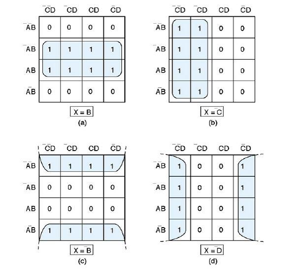
8 Karnaugh Map (K-Map) Method K Map shows the relationship between inputs & outputs Horizontally & vertically adjacent squares differ only in one variable.
9
10
11 Looping is a process combining the squares which contain 1s. The output expression can be simplified by looping.
12
13
14 Rule for loops of any size When a variable appears in both complemented & uncomplemented form within a loop, that variable is eliminated from the expression. Variables that are the same for all squares of the loop must appear in the final expression.
15 Complete Simplification Process 1.Construct the K map and place 1s and 0s in the squares according to the truth table. 2.Loop the isolated 1s which are not adjacent to any other 1s. (single loops) 3.Loop any pair which contains a 1 adjacent to only one other 1. (double loops) 4.Loop any octet even if it contains one or more 1s that have already been looped. 5.Loop any quad that contains one or more 1s that have not already been looped, making sure to use the minimum number of loops. 6.Loop any pairs necessary to include any 1s that have not yet been looped, making sure to use the minimum number of loops. 7.Form the OR sum of all the terms generated by each loop.
16
17 Don t-care Conditions are certain input conditions for which there are no specified output levels. Don t-care conditions should be changed to either 0 or 1 to produce K-map looping that yields the simplest expression.
18 Filling K-Map from Output Expression When the desired output is presented as a Boolean expression instead of a truth table, the K map can be filled by using the following steps: 1. Get the expression into SOP form if it is not already so. 2. For each product term in the SOP expression, place a 1 in each K-map square whose label contains the same combination of input variables. Place a 0 in all other squares.
19 Don t care condition can come about for several reasons: In some situations certain input combination can never occur and so there is no specified output for these condition. Whenever don t care conditions occur, we must decide which x to change to 0 and which to 1 to produce the best K-map looping (i.e the simplest expression)
20 Example
21 Example A BCD counter produces a four bit output representing the BCD code for the number of pulses hat have been applied to the counter input. For example, after 4 pulses have occurred, the counter outputs are DCBA= = 410. The counter resets to 0000 on the tenth pulse and starts counting over again. In other words, the DCBA output will never represent a number greater than 10012=910. Design the logic circuit that produces a HIGH output whenever the count is 2,3, or 9. Use K mapping and take advantage of the don t care conditions.
22 Summary Compared to the algebraic method, the K-map process is a more orderly process requiring fewer steps and always producing a minimum expression. For the circuits with large numbers of inputs (larger than four), other more complex techniques are used.
23 Exclusive-OR and Exclusive-NOR Circuits Exclusive-OR (XOR) produces a HIGH output whenever the two inputs are at opposite levels.
24 Exclusive-NOR (XNOR) produces a HIGH output whenever the two inputs are at the same level.
25
26 XNOR gate may be used to simplify circuit implementation.
27 Parity Generator and Checker
28 A transmitter can attach a parity bit to a set of data bits before transmitting the data bits to a receiver. The receiver will detect any single bit errors that may have occurred during the transmission. In figure (a) the set of data to be transmitted is applied to the parity-generator circuit, which produces the evenparity bit, P, at its output. This parity bit is transmitted to the receiver along with the original data bits, making a total of five bits. In figure (b) these five bits (data+parity) enter the receiver s parity-checker circuit, which produces an error output, E that indicates whether or not a single-bit error has occurred.
29 Enable/Disable Circuits
30 Enable/Disable Circuits cont. Ex. 1(Fig.a): Design a logic circuit that will allow a signal to pass to the output only when control inputs B and C are both HIGH; otherwise, the output will stay LOW. Ex. 2(Fig.b): Design a logic circuit that will allow a signal to pass to the output only when one, but not both, of the control inputs are HIGH; otherwise, the output will stay LOW.
 is a common type of packages.")
31 Basic Characteristics of Digital ICs Digital ICs (chips): a collection of resistors, diodes and transistors fabricated on a single piece of semiconductor materials called substrate. Dual-in-line package (DIP) is a common type of packages. It contains two parallel rows of pins.
32 Digital ICs are often categorized according to their circuit complexity as measured by the number of equivalent logic gates on the substrates. 6 levels of complexity: SSI, MSI, LSI,VLSI, ULSI,GSI. SSI having a small number of gates
33 Assignment - 15 Design a logic circuit that controls an elevator door in a three-story building. The circuit has 4 inputs. M is a logic signal that indicates when the elevator is moving (M=1) or stop (M=1).F1, F2, F3 are floor indicator signals that are normally LOW and they go HIGH only when the elevator is positioned at the level of that particular floor. For example, when the elevator is lined up level with the second floor, F2=1 and F1=F3=0. The circuit output is the open signal which is normally LOW and is to go HIGH when the elevator door is to be opened.
CHAPTER 3 BASIC & COMBINATIONAL LOGIC CIRCUIT
 CHAPTER 3 BASIC & COMBINATIONAL LOGIC CIRCUIT CHAPTER CONTENTS 3.1 Introduction to Basic Gates 3.2 Analysing A Combinational Logic Circuit 3.3 Design A Combinational Logic Circuit From Boolean Expression
Chapter 4 Combinational Logic Circuits
 Chapter 4 Combinational Logic Circuits Chapter 4 Objectives Selected areas covered in this chapter: Converting logic expressions to sum-of-products expressions. Boolean algebra and the Karnaugh map as
Chapter 4 Combinational Logic Circuits
 Chapter 4 Combinational Logic Circuits Chapter 4 Objectives Selected areas covered in this chapter: Converting logic expressions to sum-of-products expressions. Boolean algebra and the Karnaugh map as
Number system: the system used to count discrete units is called number. Decimal system: the number system that contains 10 distinguished
 Number system: the system used to count discrete units is called number system Decimal system: the number system that contains 10 distinguished symbols that is 0-9 or digits is called decimal system. As
Subject: Analog and Digital Electronics Code:15CS32
 Subject: Analog and Digital Electronics Code:15CS32 Syllabus: The Basic Gates : Review of Basic Logic gates, Positive and Negative Logic, Introduction to HDL. Combinational Logic Circuits:Sum-of-Products
University of Technology
 University of Technology Lecturer: Dr. Sinan Majid Course Title: microprocessors 4 th year Lecture 7 & 8 NAND and XOR Implementations Combinational Design Procedure NAND-NAND & NOR-NOR Networks DeMorgan
Function Table of an Odd-Parity Generator Circuit
 Implementation of an Odd-Parity Generator Circuit The first step in implementing any circuit is to represent its operation in terms of a Truth or Function table. The function table for an 8-bit data as
Digital Fundamentals
 Digital Fundamentals Tenth Edition Floyd hapter 5 Floyd, Digital Fundamentals, th ed 28 Pearson Education 29 Pearson Education, Upper Saddle River, NJ 7458. ll Rights Reserved ombinational Logic ircuits
Odd-Prime Number Detector The table of minterms is represented. Table 13.1
 Odd-Prime Number Detector The table of minterms is represented. Table 13.1 Minterm A B C D E 1 0 0 0 0 1 3 0 0 0 1 1 5 0 0 1 0 1 7 0 0 1 1 1 11 0 1 0 1 1 13 0 1 1 0 1 17 1 0 0 0 1 19 1 0 0 1 1 23 1 0 1
Digital Electronics Course Objectives
 Digital Electronics Course Objectives In this course, we learning is reported using Standards Referenced Reporting (SRR). SRR seeks to provide students with grades that are consistent, are accurate, and
Name: Class: Date: 1. As more electronic systems have been designed using digital technology, devices have become smaller and less powerful.
 Name: Class: Date: DE Midterm Review 2 True/False Indicate whether the statement is true or false. 1. As more electronic systems have been designed using digital technology, devices have become smaller
Chapter 3 Digital Logic Structures
 Chapter 3 Digital Logic Structures Transistor: Building Block of Computers Microprocessors contain millions of transistors Intel Pentium 4 (2): 48 million IBM PowerPC 75FX (22): 38 million IBM/Apple PowerPC
Analysis procedure. To obtain the output Boolean functions from a logic diagram, proceed as follows:
 Combinational Logic Logic circuits for digital systems may be combinational or sequential. combinational circuit consists of input variables, logic gates, and output variables. 1 nalysis procedure To obtain
2 Logic Gates THE INVERTER. A logic gate is an electronic circuit which makes logic decisions. It has one output and one or more inputs.
 2 Logic Gates A logic gate is an electronic circuit which makes logic decisions. It has one output and one or more inputs. THE INVERTER The inverter (NOT circuit) performs the operation called inversion
Gates and Circuits 1
 1 Gates and Circuits Chapter Goals Identify the basic gates and describe the behavior of each Describe how gates are implemented using transistors Combine basic gates into circuits Describe the behavior
Logic Circuit Design
 Logic Circuit Design we have studied Truth Tables Logic gates Logic algebra K-maps 1 All these are tools Tools Truth Tables Logic gates Logic algebra K-maps 2 All these are tools Tools Truth Tables Logic
Department of Electronics and Communication Engineering
 Department of Electronics and Communication Engineering Sub Code/Name: BEC3L2- DIGITAL ELECTRONICS LAB Name Reg No Branch Year & Semester : : : : LIST OF EXPERIMENTS Sl No Experiments Page No Study of
Logic Design I (17.341) Fall Lecture Outline
 Fall Lecture Outline") Logic Design I (17.341) Fall 2011 Lecture Outline Class # 07 October 31, 2011 / November 07, 2011 Dohn Bowden 1 Today s Lecture Administrative Main Logic Topic Homework 2 Course Admin 3 Administrative
Logic Design I (17.341) Fall 2011 Lecture Outline Class # 07 October 31, 2011 / November 07, 2011 Dohn Bowden 1 Today s Lecture Administrative Main Logic Topic Homework 2 Course Admin 3 Administrative
Laboratory Manual CS (P) Digital Systems Lab
 Digital Systems Lab") Laboratory Manual CS 09 408 (P) Digital Systems Lab INDEX CYCLE I A. Familiarization of digital ICs and digital IC trainer kit 1 Verification of truth tables B. Study of combinational circuits 2. Verification
Laboratory Manual CS 09 408 (P) Digital Systems Lab INDEX CYCLE I A. Familiarization of digital ICs and digital IC trainer kit 1 Verification of truth tables B. Study of combinational circuits 2. Verification
DELD UNIT 3. Question Option A Option B Option C Option D Correct Option A B C
 Class : S.E.Comp Matoshri College of Engineering and Research Center Nasik Department of Computer Engineering Digital Elecronics and Logic Design (DELD) UNIT - III Subject : DELD Sr. No. Question Option
Course Overview. Course Overview
 Course Overview Where does this course fit into the Electrical Engineering curriculum? Page 5 Course Overview Where does this course fit into the Computer Engineering curriculum? Page 6 3 Course Content
Gates and and Circuits
 Chapter 4 Gates and Circuits Chapter Goals Identify the basic gates and describe the behavior of each Describe how gates are implemented using transistors Combine basic gates into circuits Describe the
Digital. Design. R. Ananda Natarajan B C D
 Digital E A B C D 0 1 2 3 4 5 6 Design 7 8 9 10 11 12 13 14 15 Y R. Ananda Natarajan Digital Design Digital Design R. ANANDA NATARAJAN Professor Department of Electronics and Instrumentation Engineering
Digital Logic Circuits
 Digital Logic Circuits Let s look at the essential features of digital logic circuits, which are at the heart of digital computers. Learning Objectives Understand the concepts of analog and digital signals
EECS 150 Homework 4 Solutions Fall 2008
 Problem 1: You have a 100 MHz clock, and need to generate 3 separate clocks at different frequencies: 20 MHz, 1kHz, and 1Hz. How many flip flops do you need to implement each clock if you use: a) a ring
Digital Applications (CETT 1415) Credit: 4 semester credit hours (3 hours lecture, 4 hours lab) Prerequisite: CETT 1403 & CETT 1405
 Credit: 4 semester credit hours (3 hours lecture, 4 hours lab) Prerequisite: CETT 1403 & CETT 1405") Digital Applications () Credit: 4 semester credit hours (3 hours lecture, 4 hours lab) Prerequisite: CETT 1403 & CETT 1405 Course Description This course covers digital techniques and numbering systems,
Digital Applications () Credit: 4 semester credit hours (3 hours lecture, 4 hours lab) Prerequisite: CETT 1403 & CETT 1405 Course Description This course covers digital techniques and numbering systems,
Asst. Prof. Thavatchai Tayjasanant, PhD. Power System Research Lab 12 th Floor, Building 4 Tel: (02)
") 2145230 Aircraft Electricity and Electronics Asst. Prof. Thavatchai Tayjasanant, PhD Email: taytaycu@gmail.com aycu@g a co Power System Research Lab 12 th Floor, Building 4 Tel: (02) 218-6527 1 Chapter
2145230 Aircraft Electricity and Electronics Asst. Prof. Thavatchai Tayjasanant, PhD Email: taytaycu@gmail.com aycu@g a co Power System Research Lab 12 th Floor, Building 4 Tel: (02) 218-6527 1 Chapter
CS302 - Digital Logic Design Glossary By
 CS302 - Digital Logic Design Glossary By ABEL : Advanced Boolean Expression Language; a software compiler language for SPLD programming; a type of hardware description language (HDL) Adder : A digital
BOOLEAN ALGEBRA AND LOGIC FAMILIES
 C H A P T E R 7 Learning Objectives Unique Feature of Boolean Algebra Laws of Boolean Algebra Equivalent Switching Circuits DeMorgan s Theorem s The Sum-of-Products (SOP) Form The Standard SOP Form The
Logic Symbols with Truth Tables INVERTER A B NAND A B C NOR C A B A B C XNOR A B C A B Digital Logic 1
 Slide Logic Symbols with Truth Tables UFFER INVERTER ND NND OR NOR XOR XNOR 6.7 Digital Logic Digital logic can be described in terms of standard logic symbols and their corresponding truth tables. The
UNIT-2: BOOLEAN EXPRESSIONS AND COMBINATIONAL LOGIC CIRCUITS
 UNIT-2: BOOLEAN EXPRESSIONS AND COMBINATIONAL LOGIC CIRCUITS STRUCTURE 2. Objectives 2. Introduction 2.2 Simplification of Boolean Expressions 2.2. Sum of Products 2.2.2 Product of Sums 2.2.3 Canonical
Unit 1 Foundations in Electronics - Lesson 1.1 Introduction to Electronics Standards Essential Question Enduring Understandings
 Course: DIGITAL ELECTRONICS- PROJECT LEAD THE WAY (DE-PLTW) Year: 2017-2018 Teacher: Mr. Christopher Reynolds/ Mr. Kenneth Rice Unit 1 Foundations in Electronics - Lesson 1.1 Introduction to Electronics
Digital Fundamentals. Lab 4 EX-OR Circuits & Combinational Circuit Design
 Richland College School of Engineering & Technology Rev. 0 B. Donham Rev. 1 (7/2003) J. Horne Rev. 2 (1/2008) J. Bradbury Digital Fundamentals CETT 1425 Lab 4 EX-OR Circuits & Combinational Circuit Design
EMT1250 LABORATORY EXPERIMENT. EXPERIMENT # 4: Combinational Logic Circuits. Name: Date:
 EXPERIMENT # 4: Combinational Logic Circuits Name: Date: Equipment/Parts Needed: 5V DC Power Supply Digital Trainer (Logic Probe) Breadboard DIP Switch 7400 NAND gate 7402 NOR gate 7404 Inverter 7408 AND
Logic diagram: a graphical representation of a circuit
 LOGIC AND GATES Introduction to Logic (1) Logic diagram: a graphical representation of a circuit Each type of gate is represented by a specific graphical symbol Truth table: defines the function of a gate
DIGITAL ELECTRONICS. Methods & diagrams : 1 Graph plotting : - Tables & analysis : - Questions & discussion : 6 Performance : 3
 DIGITAL ELECTRONICS Marking scheme : Methods & diagrams : 1 Graph plotting : - Tables & analysis : - Questions & discussion : 6 Performance : 3 Aim: This experiment will investigate the function of the
Digital Electronics 8. Multiplexer & Demultiplexer
 1 Module -8 Multiplexers and Demultiplexers 1 Introduction 2 Principles of Multiplexing and Demultiplexing 3 Multiplexer 3.1 Types of multiplexer 3.2 A 2 to 1 multiplexer 3.3 A 4 to 1 multiplexer 3.4 Multiplex
6.1 In this section, you will design (but NOT build) a circuit with 4 inputs,
 a circuit with 4 inputs,") EE 2449 Experiment 6 Jack Levine and Nancy Warter-Perez //208 CALIFORNIA STATE UNIVERSITY LOS ANGELES Department of Electrical and Computer Engineering EE-2449 Digital Logic Lab EXPERIMENT 6 COMBINATIONAL
EE 2449 Experiment 6 Jack Levine and Nancy Warter-Perez //208 CALIFORNIA STATE UNIVERSITY LOS ANGELES Department of Electrical and Computer Engineering EE-2449 Digital Logic Lab EXPERIMENT 6 COMBINATIONAL
This Figure here illustrates the operation for a 2-input OR gate for all four possible input combinations.
 Course: B.Sc. Applied Physical Science (Computer Science) Year & Sem.: IInd Year, Sem - IIIrd Subject: Computer Science Paper No.: IX Paper Title: Computer System Architecture Lecture No.: 5 Lecture Title:
CS302 Digital Logic Design Solved Objective Midterm Papers For Preparation of Midterm Exam
 CS302 Digital Logic Design Solved Objective Midterm Papers For Preparation of Midterm Exam MIDTERM EXAMINATION 2011 (October-November) Q-21 Draw function table of a half adder circuit? (2) Answer: - Page
Digital Electronics. A. I can list five basic safety rules for electronics. B. I can properly display large and small numbers in proper notation,
 St. Michael Albertville High School Teacher: Scott Danielson September 2016 Content Skills Learning Targets Standards Assessment Resources & Technology CEQ: WHAT MAKES DIGITAL ELECTRONICS SO IMPORTANT
1.) If a 3 input NOR gate has eight input possibilities, how many of those possibilities result in a HIGH output? (a.) 1 (b.) 2 (c.) 3 (d.) 7 (e.
 If a 3 input NOR gate has eight input possibilities, how many of those possibilities result in a HIGH output? (a.) 1 (b.) 2 (c.) 3 (d.) 7 (e.") Name: Multiple Choice 1.) If a 3 input NOR gate has eight input possibilities, how many of those possibilities result in a HIGH output? (a.) 1 (b.) 2 (c.) 3 (d.) 7 (e.) 8 2.) The output of an OR gate with
Name: Multiple Choice 1.) If a 3 input NOR gate has eight input possibilities, how many of those possibilities result in a HIGH output? (a.) 1 (b.) 2 (c.) 3 (d.) 7 (e.) 8 2.) The output of an OR gate with
UNIT III. Designing Combinatorial Circuits. Adders
 UNIT III Designing Combinatorial Circuits The design of a combinational circuit starts from the verbal outline of the problem and ends with a logic circuit diagram or a set of Boolean functions from which
Lecture 2: Digital Logic Basis
 Lecture 2: Digital Logic Basis Xufeng Kou School of Information Science and Technology ShanghaiTech University 1 Outline Truth Table Basic Logic Operation and Gates Logic Circuits NOR Gates and NAND Gates
Digital Logic Design ELCT 201
 Faculty of Information Engineering and Technology Dr. Haitham Omran and Dr. Wassim Alexan Digital Logic Design ELCT 201 Winter 2017 Midterm Exam Second Chance Please tick the box of your major: IET MET
Lab Project #2: Small-Scale Integration Logic Circuits
 Lab Project #2: Small-Scale Integration Logic Circuits Duration: 2 weeks Weeks of 1/31/05 2/7/05 1 Objectives The objectives of this laboratory project are to design some simple logic circuits using small-scale
hij Teacher Resource Bank GCE Electronics Exemplar Examination Questions ELEC2 Further Electronics
 hij Teacher Resource Bank GCE Electronics Exemplar Examination Questions ELEC2 Further Electronics The Assessment and Qualifications Alliance (AQA) is a company limited by guarantee registered in England
LOGIC DIAGRAM: HALF ADDER TRUTH TABLE: A B CARRY SUM. 2012/ODD/III/ECE/DE/LM Page No. 1
 LOGIC DIAGRAM: HALF ADDER TRUTH TABLE: A B CARRY SUM K-Map for SUM: K-Map for CARRY: SUM = A B + AB CARRY = AB 22/ODD/III/ECE/DE/LM Page No. EXPT NO: DATE : DESIGN OF ADDER AND SUBTRACTOR AIM: To design
Digital Applications (CETT 1415) Credit: 4 semester credit hours (3 hours lecture, 4 hours lab) Prerequisite: CETT 1403 & CETT 1405
 Credit: 4 semester credit hours (3 hours lecture, 4 hours lab) Prerequisite: CETT 1403 & CETT 1405") Digital Applications (CETT 1415) Credit: 4 semester credit hours (3 hours lecture, 4 hours lab) Prerequisite: CETT 1403 & CETT 1405 Course Description This course covers digital techniques and numbering
Digital Applications (CETT 1415) Credit: 4 semester credit hours (3 hours lecture, 4 hours lab) Prerequisite: CETT 1403 & CETT 1405 Course Description This course covers digital techniques and numbering
Objective Questions. (a) Light (b) Temperature (c) Sound (d) all of these
 Light (b) Temperature (c) Sound (d) all of these") Objective Questions Module 1: Introduction 1. Which of the following is an analog quantity? (a) Light (b) Temperature (c) Sound (d) all of these 2. Which of the following is a digital quantity? (a) Electrical
Objective Questions Module 1: Introduction 1. Which of the following is an analog quantity? (a) Light (b) Temperature (c) Sound (d) all of these 2. Which of the following is a digital quantity? (a) Electrical
Chapter 1: Digital logic
 Chapter 1: Digital logic I. Overview In PHYS 252, you learned the essentials of circuit analysis, including the concepts of impedance, amplification, feedback and frequency analysis. Most of the circuits
B.C.A 2017 DIGITAL ELECTRONICS BCA104T MODULE SPECIFICATION SHEET. Course Outline
 Course Outline B.C.A 2017 DIGITAL ELECTRONICS BCA104T MODULE SPECIFICATION SHEET The purpose of the course is to teach principles of digital electronics. This course covers varieties of topics including
Dr. Nicola Nicolici COE/EE2DI4 Midterm Test #1 Oct 18, 2006
 COE/EE2DI4 Midterm Test #1 Fall 2006 Page 1 Dr. Nicola Nicolici COE/EE2DI4 Midterm Test #1 Oct 18, 2006 Instructions: This examination paper includes 10 pages and 20 multiple-choice questions starting
ECE380 Digital Logic
 ECE38 Digital Logic Optimized Implementation of Logic Functions: Karnaugh Maps and Minimum Sum-of-Product Forms Dr. D. J. Jackson Lecture 7- Karnaugh map The key to finding a minimum cost SOP or POS form
Chapter 3 Describing Logic Circuits Dr. Xu
 Chapter 3 Describing Logic Circuits Dr. Xu Chapter 3 Objectives Selected areas covered in this chapter: Operation of truth tables for AND, NAND, OR, and NOR gates, and the NOT (INVERTER) circuit. Boolean
LIST OF EXPERIMENTS. KCTCET/ /Odd/3rd/ETE/CSE/LM
 LIST OF EXPERIMENTS. Study of logic gates. 2. Design and implementation of adders and subtractors using logic gates. 3. Design and implementation of code converters using logic gates. 4. Design and implementation
Lecture 7: Digital Logic
 Lecture 7: Digital Logic Last time we introduced the concept of digital electronics i.e., one identifies a range of voltages with the value, and another range with the value But we didn t specify these
QUIZ. What do these bits represent?
 QUIZ What do these bits represent? 1001 0110 1 QUIZ What do these bits represent? Unsigned integer: 1101 1110 Signed integer (2 s complement): Fraction: IBM 437 character: Latin-1 character: Huffman-compressed
Chapter 4 Logic Functions and Gates
 Chapter 4 Logic Functions and Gates CHPTER OJECTIVES Upon successful completion of this chapter, you will be able to: Describe the basic logic functions: ND, OR, and NOT. Draw simple switch circuits to
MAHARASHTRA STATE BOARD OF TECHNICAL EDUCATION (Autonomous) (ISO/IEC Certified) SUMMER-16 EXAMINATION Model Answer
 (ISO/IEC Certified) SUMMER-16 EXAMINATION Model Answer") Important Instructions to examiners: 1) The answers should be examined by key words and not as word-to-word as given in the model answer scheme. 2) The model answer and the answer written by candidate
Important Instructions to examiners: 1) The answers should be examined by key words and not as word-to-word as given in the model answer scheme. 2) The model answer and the answer written by candidate
Exercise 1: EXCLUSIVE OR/NOR Gate Functions
 EXCLUSIVE-OR/NOR Gates Digital Logic Fundamentals Exercise 1: EXCLUSIVE OR/NOR Gate Functions EXERCISE OBJECTIVE When you have completed this exercise, you will be able to demonstrate the operation of
R & D Electronics DIGITAL IC TRAINER. Model : DE-150. Feature: Object: Specification:
 DIGITAL IC TRAINER Model : DE-150 Object: To Study the Operation of Digital Logic ICs TTL and CMOS. To Study the All Gates, Flip-Flops, Counters etc. To Study the both the basic and advance digital electronics
SRV ENGINEERING COLLEGE SEMBODAI RUKMANI VARATHARAJAN ENGINEERING COLLEGE SEMBODAI
 SEMBODAI RUKMANI VARATHARAJAN ENGINEERING COLLEGE SEMBODAI 6489 (Approved By AICTE,Newdelhi Affiliated To ANNA UNIVERSITY::Chennai) CS 62 DIGITAL ELECTRONICS LAB (REGULATION-23) LAB MANUAL DEPARTMENT OF
Formal Foundation of Digital Design
 Chapter 2: Switching Algebra and Logic Circuits 78 22 Digital Logic Design @ Department of Computer Engineering KKU. Formal Foundation of Digital Design In 854 George Boole published An investigation into
Combinational Logic. Rab Nawaz Khan Jadoon DCS. Lecturer COMSATS Lahore Pakistan. Department of Computer Science
 Combinational Logic Rab Nawaz Khan Jadoon DCS COMSATS Institute of Information Technology Lecturer COMSATS Lahore Pakistan Digital Logic and Computer Design 2 Combinational logic A combinational circuit
CMSC 2833 Lecture 26. Step Expression Justification
 omputer Organiation I. Karnaugh Maps and Minimiation MS Lecture Minimiation with Theorems onsider the Boolean function: FF(xx, yy, ) = xxʹyyʹ + xyʹʹ + xyʹ + xxxxʹ + xxxxxx Step Expression Justification.
Digital Electronic Concepts
 Western Technical College 10662137 Digital Electronic Concepts Course Outcome Summary Course Information Description Career Cluster Instructional Level Total Credits 4.00 Total Hours 108.00 This course
Multiple input gates. The AND gate
 Multiple input gates Inverters and buffers exhaust the possibilities for single-input gate circuits. What more can be done with a single logic signal but to buffer it or invert it? To explore more logic
Module 4: Design and Analysis of Combinational Circuits 1. Module-4. Design and Analysis of Combinational Circuits
 1 Module-4 Design and Analysis of Combinational Circuits 4.1 Motivation: This topic develops the fundamental understanding and design of adder, substractor, code converter multiplexer, demultiplexer etc
Number of Lessons:155 #14B (P) Electronics Technology with Digital and Microprocessor Laboratory Completion Time: 42 months
 Electronics Technology with Digital and Microprocessor Laboratory Completion Time: 42 months") PROGRESS RECORD Study your lessons in the order listed below. Number of Lessons:155 #14B (P) Electronics Technology with Digital and Microprocessor Laboratory Completion Time: 42 months 1 2330A Current
PROGRESS RECORD Study your lessons in the order listed below. Number of Lessons:155 #14B (P) Electronics Technology with Digital and Microprocessor Laboratory Completion Time: 42 months 1 2330A Current
Introduction to Digital Logic Missouri S&T University CPE 2210 Exam 1 Logistics
 Introduction to Digital Logic Missouri S&T University CPE 2210 Exam 1 Logistics Egemen K. Çetinkaya Egemen K. Çetinkaya Department of Electrical & Computer Engineering Missouri University of Science and
SYNTHESIS OF COMBINATIONAL CIRCUITS
 HPTER 6 SYNTHESIS O OMINTIONL IRUITS 6.1 Introduction oolean functions can be expressed in the forms of sum-of-products and productof-sums. These expressions can also be minimized using algebraic manipulations
Name EGR 2131 Lab #2 Logic Gates and Boolean Algebra Objectives Equipment and Components Part 1: Reading Pin Diagrams 7400 (TOP VIEW)
") Name EGR 23 Lab #2 Logic Gates and Boolean Algebra Objectives ) Become familiar with common logic-gate chips and their pin numbers. 2) Using breadboarded chips, investigate the behavior of NOT (Inverter),
Name EGR 23 Lab #2 Logic Gates and Boolean Algebra Objectives ) Become familiar with common logic-gate chips and their pin numbers. 2) Using breadboarded chips, investigate the behavior of NOT (Inverter),
EEE 301 Digital Electronics
 EEE 301 Digital Electronics Lecture 1 Course Contents Introduction to number systems and codes. Analysis and synthesis of digital logic circuits: Basic logic functions, Boolean algebra,combinational logic
UNIT-IV Combinational Logic
 UNIT-IV Combinational Logic Introduction: The signals are usually represented by discrete bands of analog levels in digital electronic circuits or digital electronics instead of continuous ranges represented
Electronics. Digital Electronics
 Electronics Digital Electronics Introduction Unlike a linear, or analogue circuit which contains signals that are constantly changing from one value to another, such as amplitude or frequency, digital
Associate In Applied Science In Electronics Engineering Technology Expiration Date:
 PROGRESS RECORD Study your lessons in the order listed below. Associate In Applied Science In Electronics Engineering Technology Expiration Date: 1 2330A Current and Voltage 2 2330B Controlling Current
Combinational Logic Circuits. Combinational Logic
 Combinational Logic Circuits The outputs of Combinational Logic Circuits are only determined by the logical function of their current input state, logic 0 or logic 1, at any given instant in time. The
Preface... iii. Chapter 1: Diodes and Circuits... 1
 Table of Contents Preface... iii Chapter 1: Diodes and Circuits... 1 1.1 Introduction... 1 1.2 Structure of an Atom... 2 1.3 Classification of Solid Materials on the Basis of Conductivity... 2 1.4 Atomic
Lab# 13: Introduction to the Digital Logic
 Lab# 13: Introduction to the Digital Logic Revision: October 30, 2007 Print Name: Section: In this lab you will become familiar with Physical and Logical Truth tables. As well as asserted high, asserted
NUMBER SYSTEM AND CODES
 NUMBER SYSTEM AND CODES INTRODUCTION:- The term digital refers to a process that is achieved by using discrete unit. In number system there are different symbols and each symbol has an absolute value and
Winter 14 EXAMINATION Subject Code: Model Answer P a g e 1/28
 Subject Code: 17333 Model Answer P a g e 1/28 Important Instructions to examiners: 1) The answers should be examined by key words and not as word-to-word as given in the model answer scheme. 2) The model
GUJARAT TECHNOLOGICAL UNIVERSITY, AHMEDABAD, GUJARAT COURSE CURRICULUM. Course Title: Digital Electronics (Code: )
") GUJARAT TECHNOLOGICAL UNIVERSITY, AHMEDABAD, GUJARAT COURSE CURRICULUM Course Title: Digital Electronics (Code: 3322402) Diploma Programmes in which this course is offered Semester in which offered Power
GUJARAT TECHNOLOGICAL UNIVERSITY, AHMEDABAD, GUJARAT COURSE CURRICULUM Course Title: Digital Electronics (Code: 3322402) Diploma Programmes in which this course is offered Semester in which offered Power
Fan in: The number of inputs of a logic gate can handle.
 Subject Code: 17333 Model Answer Page 1/ 29 Important Instructions to examiners: 1) The answers should be examined by key words and not as word-to-word as given in the model answer scheme. 2) The model
Combinational logic. ! Regular logic: multiplexers, decoders, LUTs and FPGAs. ! Switches, basic logic and truth tables, logic functions
 Combinational logic! Switches, basic logic and truth tables, logic functions! Algebraic expressions to gates! Mapping to different gates! Discrete logic gate components (used in labs and 2)! Canonical
Digital Systems Principles and Applications TWELFTH EDITION. 3-3 OR Operation With OR Gates. 3-4 AND Operations with AND gates
 Digital Systems Principles and Applications TWELFTH EDITION CHAPTER 3 Describing Logic Circuits Part -2 J. Bernardini 3-3 OR Operation With OR Gates An OR gate is a circuit with two or more inputs, whose
DEPARTMENT OF ELETRONICS AND COMMUNICATION ENGINEERING COURSE NOTES FACULTY NAME/DESIGNATION: SUGAPRIYAA.THA / LECTURER
 DEPARTMENT OF ELETRONICS AND COMMUNICATION ENGINEERING COURSE NOTES SUBJECT: DIGITAL ELECTRONICS SUBJECT CODE: EC2203 FACULTY NAME/DESIGNATION: SUGAPRIYAA.THA / LECTURER CLASS: II YEAR ECE UNIT-I MINIMISATION
16 Multiplexers and De-multiplexers using gates and ICs. (74150, 74154)
") 16 Multiplexers and De-multiplexers using gates and ICs. (74150, 74154) Aim: To design multiplexers and De-multiplexers using gates and ICs. (74150, 74154) Components required: Digital IC Trainer kit,
16 Multiplexers and De-multiplexers using gates and ICs. (74150, 74154) Aim: To design multiplexers and De-multiplexers using gates and ICs. (74150, 74154) Components required: Digital IC Trainer kit,
COMPUTER ORGANIZATION & ARCHITECTURE DIGITAL LOGIC CSCD211- DEPARTMENT OF COMPUTER SCIENCE, UNIVERSITY OF GHANA
 COMPUTER ORGANIZATION & ARCHITECTURE DIGITAL LOGIC LOGIC Logic is a branch of math that tries to look at problems in terms of being either true or false. It will use a set of statements to derive new true
Hashemite University Mechatronics Engineering Department Logic and Electronics Laboratory Manual
 Hashemite University Mechatronics Engineering Department Logic and Electronics Laboratory Manual The Hashemite University Faculty of Engineering Department of Mechatronics Engineering Logic and Electronics
EECS-140/141 Introduction to Digital Logic Design Lecture 4:Simplification in Logic Synthesis
 EECS-140/141 Introduction to Digital Logic Design Lecture 4:Simplification in Logic Synthesis I. REVIEW AND INTRODUCTION I.A General Synthesis Procedure I.A.1 Express Function as: I.A.1.a Define variables
Government of Karnataka Department of Technical Education Board of Technical Examinations, Bengaluru
 Prerequisites Government of Karnataka Department of Technical Education Board of Technical Examinations, Bengaluru Course Title :Digital Electronics Lab I Course Code : 15EC2P Semester : II Course Group
Positive and Negative Logic
 Course: B.Sc. Applied Physical Science (Computer Science) Year & Sem.: IInd Year, Sem - IIIrd Subject: Computer Science Paper No.: IX Paper Title: Computer System Architecture Lecture No.: 4 Lecture Title:
COMBINATIONAL and SEQUENTIAL LOGIC CIRCUITS Hardware implementation and software design
 PH-315 COMINATIONAL and SEUENTIAL LOGIC CIRCUITS Hardware implementation and software design A La Rosa I PURPOSE: To familiarize with combinational and sequential logic circuits Combinational circuits
2 Building Blocks. There is often the need to compare two binary values.
 2 Building Blocks 2.1 Comparators There is often the need to compare two binary values. This is done using a comparator. A comparator determines whether binary values A and B are: 1. A = B 2. A < B 3.
S-[F] NPW-02 June All Syllabus B.Sc. [Electronics] Ist Year Semester-I & II.doc - 1 -
![S-[F] NPW-02 June All Syllabus B.Sc. [Electronics] Ist Year Semester-I & II.doc - 1 -](/thumbs/79/79759849.jpg "S-[F] NPW-02 June All Syllabus B.Sc. [Electronics] Ist Year Semester-I & II.doc - 1 -") - 1 - - 2 - - 3 - DR. BABASAHEB AMBEDKAR MARATHWADA UNIVERSITY, AURANGABAD SYLLABUS of B.Sc. FIRST & SECOND SEMESTER [ELECTRONICS (OPTIONAL)] {Effective from June- 2013 onwards} - 4 - B.Sc. Electronics
- 1 - - 2 - - 3 - DR. BABASAHEB AMBEDKAR MARATHWADA UNIVERSITY, AURANGABAD SYLLABUS of B.Sc. FIRST & SECOND SEMESTER [ELECTRONICS (OPTIONAL)] {Effective from June- 2013 onwards} - 4 - B.Sc. Electronics
In this lecture: Lecture 8: ROM & Programmable Logic Devices
 In this lecture: Lecture 8: ROM Programmable Logic Devices Dr Pete Sedcole Department of EE Engineering Imperial College London http://caseeicacuk/~nps/ (Floyd, 3 5, 3) (Tocci 2, 24, 25, 27, 28, 3 34)
NORTH MAHARASHTRA UNIVERSITY. F.Y. B. Sc. Electronics. Syllabus. Wieth effect from june2015
 Syllabus Wieth effect from june2015 Paper- I, Semester I ELE-111: Analog Electronics I Unit- I:Introduction to Basic Circuit Components Definition and unit, Circuit Symbol, Working Principle, Classification
THE UNIVERSITY OF TRINIDAD & TOBAGO
 THE UNIVERSITY OF TRINIDAD & TOBAGO FINAL ASSESSMENT/EXAMINATIONS APRIL/MAY 2014 Course Code and Title: Digital Electronics Programme: Communications Engineering Technology Diploma Date: 16 th April 2014
Fig.16.1: Digital systems and analog systems
 UNIT 16 LOGIC GATES Structure Introduction Objectives Boolean Algebra Logic Gates AND Gate OR Gate NOT Gate NAND Gate NOR Gate NAND and NOR Gates as Universal Gates Circuits for Logic Gates Elementary