hij Teacher Resource Bank GCE Electronics Exemplar Examination Questions ELEC2 Further Electronics
|
|
|
- Moris Holland
- 5 years ago
- Views:
Transcription
 and a registered charity (registered charity number 1073334). Registered address: AQA, Devas Street, Manchester M15 6EX.")
1 hij Teacher Resource Bank GCE Electronics Exemplar Examination Questions ELEC2 Further Electronics The Assessment and Qualifications Alliance (AQA) is a company limited by guarantee registered in England and Wales (company number ) and a registered charity (registered charity number ). Registered address: AQA, Devas Street, Manchester M15 6EX. Dr Michael Cresswell, Director General.
2 ELEC2 Further Electronics Capacitors in Series and Time Constant (ELE1, Q3, 2007) klm 1
3 Capacitors in Parallel and Time Constant (ELE1, Q3, 2006) 2 klm
4 Time Constant (ELE1, Q2, 2008) klm 3
5 Time Constant and Capacitors in Parallel (ELE1, Q2, 2005) 4 klm
6 555 Monostable and Relay (ELE1, Q7, 2005 ELE1, Q6, 2006) klm 5
7 6 klm
8 555 Astable (ELE1, Q4, 2005 ELE1, Q5, 2007) klm 7
9 8 klm
10 Comparator and 555 Astable (ELE1, Q5, 2008) klm 9
11 10 klm
12 Shift Register (ELE2, Q6, 2005 ELE2, Q6, 2008 ELE2, Q6, 2007) klm 11
13 12 klm
14 klm 13
15 14 klm
16 klm 15
17 16 klm
18 NAND Gate Bistable (ELE2, Q1, 2006) klm 17
19 NAND Gate Bistable and MOSFET (ELE2, Q3, 2005) (3 marks) 18 klm
20 Counter and Boolean (ELE2, Q5, 2005) klm 19
21 (3 marks) 20 klm
22 Counter (ELE2, Q1, 2007) (4 marks) klm 21
23 22 klm
24 Non-Inverting Amplifier (ELE2, Q2, 2008) klm 23
25 24 klm
26 Voltage Follower, Summing Amplifier, Inverting Amplifier (ELE2, Q6, 2006) klm 25
27 26 klm
28 klm 27
29 Inverting and Summing Amplifiers (ELE2, Q5, 2007) 28 klm
30 klm 29
31 Summing Amplifier (ELE2, Q4, 2005) 30 klm
32 klm 31
33 Power Amp (ELE2, Q4, 2008 ELE2, Q7, 2007 ELE2, Q7, 2005 ELE2, Q4, 2006) 32 klm
34 klm 33
35 34 klm
36 klm 35
37 36 klm
38 klm 37
39 38 klm
40 klm 39
41 40 klm
42 klm 41
43 42 klm
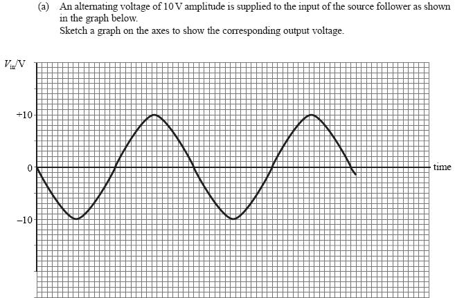
44 Op-Amp and Source Follower (ELE2, Q3, 2008) klm 43
45 44 klm
46 MOSFET Source Follower / Constant Current Generator (ELE2, Q4, 2007) klm 45
47 46 klm
48 MOSFET Source Follower and Non-Inverting Amplifier (ELE2, Q5, 2006) klm 47
49 48 klm
50 This page is intentionally blank
51 hij Teacher Resource Bank GCE Electronics Exemplar Exam Questions Mark Scheme ELEC2: Further Electronics The Assessment and Qualifications Alliance (AQA) is a company limited by guarantee registered in England and Wales (company number ) and a registered charity (registered charity number ). Registered address: AQA, Devas Street, Manchester M15 6EX. Dr Michael Cresswell, Director General.
52 Teacher Resource Bank / GCE Electronics / ELEC2 Sample Questions Mark Scheme / Version 1.0 Capacitor in Series and Time Constant (ELE1, Q3, 2007) 3 (a) (i) , or (68 68) ( ) = 34μF (ii) = 5.1s (4 marks) (b) (i) T = 0.69RC, = 3.5s (ii) 5RC = 5 x 5.1 = 25.5s (3 marks) (Total 7 marks) Capacitors in Parallel and Time Constant (ELE1, Q3, 2006) 3 (a) (i) I = V/R = 12/10 4 = 1.2 ma (ii) = 3200μF (iii) T = RC = 10 4 x 3.2 x 10-3 = 32s (5 marks) (b) (i) 6/12 = ½ Vs T = 0.69RC 0.69 x 32 = 22s (ii) 5RC = 5 x 32 = 160s (5 marks) (question total 10 marks) Time Constant (ELE1, Q2, 2008) 2 (a) (i) = 27mA (ii) = 0.25W (b) (i) = 0.155s (ii) 5RC = 0.78s (iii) T = = 4.7s 5RC = 23.5s Total 10 Time Constant and Capacitors in Parallel (ELE1, Q2, 2005) 2 (a) (i) = 69 μf (ii) 69 x = 13.8 s (3 marks) (b) (i) 0.69 x 13.8 = 9.5 s (ii) 5 x 13.8 = 69 s (4 marks) Total 7 marks 2
53 Teacher Resource Bank / GCE Electronics / ELEC2 Sample Questions Mark Scheme / Version Monostable and Relay (ELE1, Q7, 2005 ELE1, Q6, 2006) 7 (a) 1.1 x 680 k x 470 μf = 350 s (2 marks) 6 (a) (b) negative going (1 mark) (c) NO (1 mark) (d) diode across coil in inverse parallel (1 mark) Total 5 marks +V s 150k reset +V s 555 IC discharge input threshold trigger output + 470μF (b) 1.1 RC = 1.1 x 1.5 x 10 5 x 4.7 x 10-4 = 77.5s 0V (6 marks) (2 marks) (c) COM and NO (any order) (2 marks) (question total 10 marks) 3
54 Teacher Resource Bank / GCE Electronics / ELEC2 Sample Questions Mark Scheme / Version Astable (ELE1, Q4, 2005 ELE1, Q5, 2007) 4 (a) +12 V R A 1 kω reset V s discharge R B 2.2 kω threshold output output trigger ground control voltage C 1000 μf 0 V (6 marks) (b) (i) 0.7 x 2.2 x 10 3 x 10 3 = 1.54 s (ii) 0.7 x 3.2 x 10 3 x 10 3 = 2.24 s (4 marks) Total 10 marks 4
55 Teacher Resource Bank / GCE Electronics / ELEC2 Sample Questions Mark Scheme / Version (a) (i) (ii) +9V R A 10kΩ reset +V s 555 IC R B 10kΩ discharge threshold output trigger C + 100μF 0V (6 marks) (b) (i) t h = = 1.4s (ii) t l = = 0.7s (iii) f = 1.44 ( )= 0.5Hz (6 marks) (Total 12 marks) Comparitor and 555 Astable (ELE1, Q5, 2008) 5 (a) astable NOR gate LED sound sensor comparator (b) (i) comparator 5
56 Teacher Resource Bank / GCE Electronics / ELEC2 Sample Questions Mark Scheme / Version 1.0 (ii) astable (c) (i) (1 1501) 9V = 6mV (ii) 9V or high (iii) 0V or low (d) (i) +V s R A 100k reset +V s 555 IC R B 22kΩ discharge threshold output trigger C 0V (ii) C = Hz = 5μF Total 18 Sheft Register (ELE2, Q6, 2005 ELE2, Q6, 2008 ELE2, Q6, 2007) 6 (a) On the rising edge of each clock pulse The data from a D-type flip-flop is stored in the next D-type flip-flop This data transfer occurs all of the way along the shift register New data applied to the input of the first flip-flop is taken into the shift register (4 marks) (b) Removes multiple pulses due to contact bounce (1 mark) 6
57 Teacher Resource Bank / GCE Electronics / ELEC2 Sample Questions Mark Scheme / Version 1.0 (c) (d) The D input of the first flip-flop goes to logic 1 The clock input goes to logic 1 and the data is shifted along the shift register (2 marks) The output of the five input AND gate must be logic 1 =>10001 The Q output of the last flip-flop must also be logic 1 => smallest binary number is (2 marks) Total 9 marks 6 (a) For each flip-flop Q becomes D On the rising edge of the clock pulse Since D is connected to the previous Q, data is moved along the shift register (on each clock pulse) (b) (i) Making S logic 0 will not set Q to 0 => the shift register must be reset before the parallel data is loaded (ii) Logic 1 (c) output 1 (Initially at logic 1) (General overall shape) clock pulse Total 9 6 (a) (i) CKs all connected together, Resets all connected together, D to proceeding Q Input to D A (ii) switch to +V s, pull down resistor to 0V (6 marks) (b) 12 => 1100 => C => appropriate symbol for C 13 => 1101 => D => appropriate symbol for d 15 => 1111 => F => appropriate symbol for F OR (3 marks) (Total 9 marks) 7
58 Teacher Resource Bank / GCE Electronics / ELEC2 Sample Questions Mark Scheme / Version 1.0 NAND Gate Bistable (ELE2, Q1, 2006) 1 (a) (i) One input from gate 1 to output of gate 2, one input from gate 2 to output of gate 1 Pull up resistors on the two free inputs (3 marks) (ii) Correct points labelled as outputs Q and Q SET on input opposite Q RESET in input opposite Q (3 marks) (b) When the SET input is briefly taken to logic 0 The Q output will become logic 1 and the Q output will become logic 0 When the RESET input is now briefly taken to logic 0, Q will become logic 0 and the Q will become logic 1 (3 marks) (question total 9 marks) NAND Gate Bistable and MOSFET (ELE2, Q3, 2005) 3 (a) A bistable latch Q B Q (2 marks) (b) (i) 0 (ii) 0 (iii) 1 (iv) 1 (4 marks) 8
59 Teacher Resource Bank / GCE Electronics / ELEC2 Sample Questions Mark Scheme / Version 1.0 (c) +12V water valve from Q 0V 0V (3 marks) Total 9 marks Counter and Boolean (ELE2, Q5, 2005) 5 (a) Q A Q B Q C Q D clock D >CK R Q A D Q B D Q C D Q D >CK >CK >CK Q R Q R Q R Q (b) D to Q All Resets joined together Q to following CK Output of AND gate to Reset B and D to inputs of AND gate Binary values for when the heater is on: 0010, 0101, 0111, 1000 The counter outputs ANDed together to form the binary values which are then ORed (4 marks) (2 marks) 9
60 Teacher Resource Bank / GCE Electronics / ELEC2 Sample Questions Mark Scheme / Version 1.0 (c) D.C.B.A + D.C.B.A + D.C.B.A + D.C.B.A = D.C.B.A + D.C.B.A + D.C.A. = C.A D.B = C.A D ( + D.B) + D.C.A ( B) + D.C. A ( B + B) (3 marks) Total 9 marks Counter (ELE2, Q1, 2007) 1 (a) D to Q Q to next clock C to AND gate input D to AND gate input AND output connected to all resets (max 4 marks) (b) (i) Each term represents one line within the truth table for which the output is 1 Each letter within each term represents the logic state of the counter outputs (ii) Correct use of either Karnaugh Map of Boolean algebra At least one piece of simplification Simplification to D.C.A + D.C. B (5 marks) (Total 9 marks) Non-Inverting Amplifier (ELE2, Q2, 2008) 2 (a) (i) V = I x R = 10 7 x 2 x = 2 x 10⁻³ V (ii) G v = V out / V in = 200 x 10-3 / 2 x 10-3 = 100 (b) Very high impedance (resistance) input This will not shunt the 10MΩ resistor of the ionisation chamber so lowering the output voltage (c) (i) Inverting amp connection to junction of 10MΩ resistor and R (ii) (Gv = 1 + Rf / R) => 100 = / R =>R = 10 7 / 99 = 101kΩ Total 9 10
61 Teacher Resource Bank / GCE Electronics / ELEC2 Sample Questions Mark Scheme / Version 1.0 Voltage Follower, Summing Amplifier, Inverting Amplifier (ELE2, Q6, 2006) 6 (a) (i) 1 (1 mark) (ii) 1MΩ (1 mark) (b) (i) -1 (1 mark) (ii) amplitude x 10 inverted (2 marks) (c) (i) inverting input terminal of op-amp (1 mark) (ii) +0.7V -0.7V (2 marks) (iii) volume (level) control (1 mark) (question total 9 marks) Inverting and Summing Amplifiers (ELE2, Q5, 2007) 5 (a) correctly connected inputs, feedback resistor in correct place, realistic values of R - accept between 1kΩ and 1MΩ, both Rs the same. input +9V + 9V output 0V 0V (b) (i) Any appropriate place associated with inverting input of op-amp (Accept if not X!) (4 marks) (ii) Appropriate calculation leading to answer e.g v v Output voltage = (+)200v (3 marks) (c) (i) Calculation leading to answer of 1.99kg (ii) Resolution of meter is 0.01V => smallest change in weight is 0.01kg or 10g (2 marks) (Total 9 marks) 11
62 Teacher Resource Bank / GCE Electronics / ELEC2 Sample Questions Mark Scheme / Version 1.0 Summing Amplifier (ELE2, Q4, 2005) 4 (a) input A input B 30kΩ 30kΩ P _ 15kΩ +12V + 12V output (b) 0V V out = R f {V a /R a + V b /R b } V out = 15{2/30 + 0/30} = 1V 0V (1 mark) (2 marks) (c) V out = 15{2/30 + 2/30} = 2V (1 mark) (d) (i) The magnitude of the signal is not altered The signal is inverted (ii) Signal 2 is inverted which makes the audio in phase with signal 1 The noise on signal 2 is inverted compared to that on signal 1 When added together the noise signals cancel (5 marks) Total 9 marks Power Amp (ELE2, Q4, 2008 ELE2, Q7, 2007 ELE2, Q7, 2005 ELE2, Q4, 2006) 4 (a) Inverting amplifier with a voltage gain of 200 / 10 = 20 So with a 500mV input the output will be 10V (b) P rms = V p 2 / 2 x R = 10 2 / 2 x 8 = 100 / 16 = 6.25W (c) (i) Cross over distortion, when neither of the output transistors conducts at small (input) output voltages (ii) Diode biasing networks to turn on the output transistors Push-pull stage included in the (negative) feedback loop (d) Large surface area Dark, matt colour Good conductor of heat (max 2) Total 9 12
63 Teacher Resource Bank / GCE Electronics / ELEC2 Sample Questions Mark Scheme / Version (a) (i) G v = V out / V in = 15 / = 200 (ii) 6 x 10 5 = f x G v = f x 200 =>f = 6 x 10 5 / 200 = 3000Hz (b) (i) 1MΩ Assuming input impedance of capacitor is negligible (or input impedance of op-amp is very large) (ii) Assume source followers have a voltage gain of 1 G v = 1 + R f / R = 1 + R f / 10 4 R f = 1.99 x 10 6 (allow 2MΩ) (2 marks) (6 marks) (c) (i) X-over distortion is non-linearity in the characteristic of the amplifier when the signal changes from positive to negative or vice versa (ii) No - because the MOSFETs are biased into conduction (mention of 50mA drain current) (because of the negative feedback loop) (3 marks) (d) (i) P out = V 2 s / 2 x R = 15 2 / 8 = W (ii) Output of op-amp does not reach saturation at the supply voltages MOSFETs have V gs when conducting (4 marks) (e) Dark colour (to aid radiation) Large surface area (to aid radiation and convection) Made of metal (to aid conduction) (fan (to assist convection) ) (max 3 marks) (Total 18 marks) 13
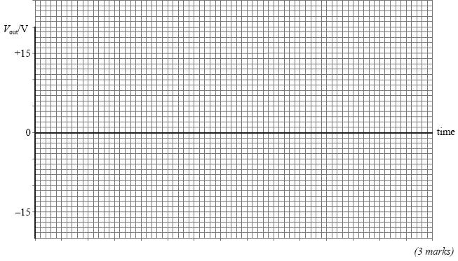
64 Teacher Resource Bank / GCE Electronics / ELEC2 Sample Questions Mark Scheme / Version (a) V in /V time 10 V out /V +15 8V 0 time 15 (3 marks) (b) (i) Push Pull (ii) Inverting amplifier with G v of 4.7 and source follower with Gv of 1 => Overall G v = 4.7 x 1 = 4.7 (3 marks) (c) (i) Cross-over distortion (ii) When the input voltage is smaller than that needed to make either MOSFET conduct (iii) 0 Amps V gs is only 1.36V => MOSFETs are not conducting (4 marks) (d) There needs to be approx 2V across each 1kΩ resistor So there must be 13V across (X) (Y) => 2mA through 1kΩ resistor => (X) (Y) = 6.5kΩ (3 marks) (e) Include MOSFETs into feedback loop by disconnecting 47kΩ resistor from op-amp output and connecting to MOSFET output (2 marks) (f) P = V s 2 /2R => P = 15 2 /2 x 4 = 28W If take into account V gs of MOSFETs ie P = 13 2 / 2 x 4 = 21W (3 marks) Total 18 marks 14
65 Teacher Resource Bank / GCE Electronics / ELEC2 Sample Questions Mark Scheme / Version (a) Push-pull. The signal is split into positive and negative going signals These are amplified separately and then recombined to recreate the amplified signal (b) (i) Power supply voltage is not large enough (Gain too large) (Saturation or clipping) (2 marks) (1 mark) (ii) Maximum output voltage is 15V Max power = V P 2 / 2xR = 15 2 / 2x4 = 225 / 8 = 28W (2 marks) (c) (iii) Power = I 2 R => 28 = I 2.4 =>I = 7 = 2.65A rms voltage = 18 / = 12.73V Power supplied = V rms x I rms = x 2.65 = 33.7W (1 marks) (2 marks) (d) Energy dissipated as heat in the output transistors (1 marks) (question total 9 marks) Op-Amp and Source Follower (ELE2, Q3, 2008) 3 (a) (i) On the line joining the MOSFET to the transmitter (ii) (Source) follower (common drain amplifier) (b) (i) Voltage divider OR 12V in the ratio of 1 : 2 Calculation => Voltage at non-inverting input is 8V (ii) Negative feedback attempts to reduce the difference between the two inputs to zero. => In the absence of an input signal both inputs will be at 8V so the output must be at 8V (iii) Two volts appear across the gate to source of the MOSFET so there will be 6V across the rf amplifier (c) (i) G v = -R f / R 1 = -470 / 10 = (-)47 (ii) If input is 40mV, then op-amp output is 1.88V Assume G v of source follower is 1 the voltage change across rf amplifier is also 1.88V Total 9 15
66 Teacher Resource Bank / GCE Electronics / ELEC2 Sample Questions Mark Scheme / Version 1.0 MOSFET Source Follower / Constant Current Generator (ELE2, Q4, 2007) 4 (a) very large open loop voltage gain so there must only be a very small difference in inputs if output is not to be saturated (2 marks) (b) If 200mA passes through battery it must also pass through R R = V / I => R = 5/0.2 = 25Ω (2 marks) (c) (i) source follower (or equivalent) (ii) The op-amp will not supply such a large current (2 marks) (d) As the battery voltage rises, the output of the op-amp will also rise so as to ensure that there is 200mA passing through the battery and R and so maintaining the 5V across R and hence 5V at its own input terminals (3 marks) (Total 9 marks) MOSFET Source Follower and Non-inverting Amplifier (ELE2, Q5, 2006) 5 (a) source follower (1 mark) (b) (c) The output voltage of the op-amp will be 0V and there will be a voltage drop of 0.7V across the diode, so making the gate of the MOSFET -0.7V 2V The characteristic shows that a drain to source current only passes when Vgs is greater than 2V (1 mark) (2 marks) (d) (i) positive parts of the output signal pass to the gate via the diode, causing the capacitor to charge and so increasing the gate voltage (1 mark) (ii) increases the brightness of the lamp (1 mark) 16
67 Teacher Resource Bank / GCE Electronics / ELEC2 Sample Questions Mark Scheme / Version 1.0 (iii) (iv) decreases the resistance of the LDR decreases the voltage gain of the amplifier (1 mark) (1 mark) (e) automatic volume control (1 mark) (question total 9 marks) 17
GCE Electronics Exemplar Exam Questions ELEC5: Communication Systems
 hij Teacher Resource Bank GCE Electronics Exemplar Exam Questions ELEC5: Communication Systems The Assessment and Qualifications Alliance (AQA) is a company limited by guarantee registered in England and
ELE1. ELECTRONICS Unit 1 Foundation Electronics. General Certificate of Education June 2004 Advanced Subsidiary Examination
 Surname Centre Number Other Names Candidate Number Leave blank Candidate Signature General Certificate of Education June 2004 Advanced Subsidiary Examination ELECTRONICS Unit 1 Foundation Electronics ELE1
ELEC2 (JUN15ELEC201) General Certificate of Education Advanced Subsidiary Examination June Further Electronics TOTAL. Time allowed 1 hour
 General Certificate of Education Advanced Subsidiary Examination June Further Electronics TOTAL. Time allowed 1 hour") Centre Number Surname Candidate Number For Examiner s Use Other Names Candidate Signature Examiner s Initials Question Mark Electronics General Certificate of Education Advanced Subsidiary Examination
Centre Number Surname Candidate Number For Examiner s Use Other Names Candidate Signature Examiner s Initials Question Mark Electronics General Certificate of Education Advanced Subsidiary Examination
GCSE (9-1) WJEC Eduqas GCSE (9-1) in ELECTRONICS ACCREDITED BY OFQUAL DESIGNATED BY QUALIFICATIONS WALES SAMPLE ASSESSMENT MATERIALS
 WJEC Eduqas GCSE (9-1) in ELECTRONICS ACCREDITED BY OFQUAL DESIGNATED BY QUALIFICATIONS WALES SAMPLE ASSESSMENT MATERIALS") GCSE (9-1) WJEC Eduqas GCSE (9-1) in ELECTRONICS ACCREDITED BY OFQUAL DESIGNATED BY QUALIFICATIONS WALES SAMPLE ASSESSMENT MATERIALS Teaching from 2017 For award from 2019 GCSE ELECTRONICS Sample Assessment
GCSE (9-1) WJEC Eduqas GCSE (9-1) in ELECTRONICS ACCREDITED BY OFQUAL DESIGNATED BY QUALIFICATIONS WALES SAMPLE ASSESSMENT MATERIALS Teaching from 2017 For award from 2019 GCSE ELECTRONICS Sample Assessment
GCE AS. WJEC Eduqas GCE AS in ELECTRONICS ACCREDITED BY OFQUAL DESIGNATED BY QUALIFICATIONS WALES SAMPLE ASSESSMENT MATERIALS
 GCE AS WJEC Eduqas GCE AS in ELECTRONICS ACCREDITED BY OFQUAL DESIGNATED BY QUALIFICATIONS WALES SAMPLE ASSESSMENT MATERIALS Teaching from 207 For award from 208 AS ELECTRONICS Sample Assessment Materials
GCSE Electronics. Scheme of Work
 GCSE Electronics Scheme of Work Week Topic Detail Notes 1 Practical skills assemble a circuit using a diagram recognize a component from its physical appearance (This is a confidence building/motivating
Draw in the space below a possible arrangement for the resistor and capacitor. encapsulated components
 1). An encapsulated component is known to consist of a resistor and a capacitor. It has two input terminals and two output terminals. A 5V, 1kHz square wave signal is connected to the input terminals and
HIGH LOW Astable multivibrators HIGH LOW 1:1
 1. Multivibrators A multivibrator circuit oscillates between a HIGH state and a LOW state producing a continuous output. Astable multivibrators generally have an even 50% duty cycle, that is that 50% of
Process Components. Process component
 What are PROCESS COMPONENTS? Input Transducer Process component Output Transducer The input transducer circuits are connected to PROCESS COMPONENTS. These components control the action of the OUTPUT components
Electronics (JUN ) General Certificate of Secondary Education June Time allowed 2 hours TOTAL
 General Certificate of Secondary Education June Time allowed 2 hours TOTAL") Centre Number Surname Candidate Number For Examiner s Use Other Names Candidate Signature Examiner s Initials Question Mark General Certificate of Secondary Education June 2012 Electronics 44301 1 2 3
Centre Number Surname Candidate Number For Examiner s Use Other Names Candidate Signature Examiner s Initials Question Mark General Certificate of Secondary Education June 2012 Electronics 44301 1 2 3
Monday 13 June 2016 Afternoon Time allowed: 2 hours
 Please write clearly in block capitals. Centre number Candidate number Surname Forename(s) Candidate signature GCSE ELECTRONICS Unit 1 Written Paper Monday 13 June 2016 Afternoon Time allowed: 2 hours
GOVERNMENT OF KARNATAKA KARNATAKA STATE PRE-UNIVERSITY EDUCATION EXAMINATION BOARD II YEAR PUC EXAMINATION MARCH-2013 SCHEME OF VALUATION
 GOVERNMENT OF KARNATAKA KARNATAKA STATE PRE-UNIVERSITY EDUCATION EXAMINATION BOARD II YEAR PUC EXAMINATION MARCH-03 SCHEME OF VALUATION Subject Code: 0 Subject: PART - A 0. What does the arrow mark indicate
ELEXBO A-Car-Engineering
 1 Task: -Construct successively all schematic diagrams and describe your findings. -Describe also the differences between the previous electrical diagram. Construct this electrical circuit and describe
Multivibrators. Department of Electrical & Electronics Engineering, Amrita School of Engineering
 Multivibrators Multivibrators Multivibrator is an electronic circuit that generates square, rectangular, pulse waveforms. Also called as nonlinear oscillators or function generators. Multivibrator is basically
ELECTRONICS ADVANCED SUPPLEMENTARY LEVEL
 ELECTRONICS ADVANCED SUPPLEMENTARY LEVEL AIMS The general aims of the subject are : 1. to foster an interest in and an enjoyment of electronics as a practical and intellectual discipline; 2. to develop
UNIT E1 (Paper version of on-screen assessment) A.M. WEDNESDAY, 8 June hour
 A.M. WEDNESDAY, 8 June hour") Candidate Name GCSE 46/0 Centre Number Candidate Number 0 ELECTRONICS UNIT E (Paper version of on-screen assessment) A.M. WEDNESDAY, 8 June 20 hour For s use 46 0000 Total Mark ADDITIONAL MATERIALS Information
Candidate Name GCSE 46/0 Centre Number Candidate Number 0 ELECTRONICS UNIT E (Paper version of on-screen assessment) A.M. WEDNESDAY, 8 June 20 hour For s use 46 0000 Total Mark ADDITIONAL MATERIALS Information
OCR ADVANCED SUBSIDIARY GCE IN ELECTRONICS (3826) OCR ADVANCED GCE IN ELECTRONICS (7826) Specimen Question Papers and Mark Schemes
 OCR ADVANCED GCE IN ELECTRONICS (7826) Specimen Question Papers and Mark Schemes") OCR ADVANCED SUBSIDIARY GCE IN ELECTRONICS (3826) OCR ADVANCED GCE IN ELECTRONICS (7826) Specimen Question Papers and Mark Schemes These specimen assessment materials are designed to accompany the OCR
OCR ADVANCED SUBSIDIARY GCE IN ELECTRONICS (3826) OCR ADVANCED GCE IN ELECTRONICS (7826) Specimen Question Papers and Mark Schemes These specimen assessment materials are designed to accompany the OCR
ELECTRONICS ELEC1. Mark scheme June 2016 INTRODUCTORY ELECTRONICS. Version: 1.0 Final
 AS ELECTRONICS ELEC INTRODUCTORY ELECTRONICS Mark scheme June 06 Version:.0 Final MARK SCHEME AS ELECTRONICS ELEC JUNE 06 Mark schemes are prepared by the Lead Assessment Writer and considered, together
Analog Electronic Circuits Lab-manual
 2014 Analog Electronic Circuits Lab-manual Prof. Dr Tahir Izhar University of Engineering & Technology LAHORE 1/09/2014 Contents Experiment-1:...4 Learning to use the multimeter for checking and indentifying
CHAPTER 6 DIGITAL INSTRUMENTS
 CHAPTER 6 DIGITAL INSTRUMENTS 1 LECTURE CONTENTS 6.1 Logic Gates 6.2 Digital Instruments 6.3 Analog to Digital Converter 6.4 Electronic Counter 6.6 Digital Multimeters 2 6.1 Logic Gates 3 AND Gate The
GOVERNMENT OF KARNATAKA KARNATAKA STATE PRE-UNIVERSITY EDUCATION EXAMINATION BOARD II YEAR PUC EXAMINATION JULY-2012 SCHEME OF VALUATION
 GOVERNMENT OF KARNATAKA KARNATAKA STATE PRE-UNIVERSITY EDUCATION EXAMINATION BOARD II YEAR PUC EXAMINATION JULY-0 SCHEME OF VALUATION Subject Code: 40 Subject: PART - A 0. Which region of the transistor
B.E. SEMESTER III (ELECTRICAL) SUBJECT CODE: X30902 Subject Name: Analog & Digital Electronics
 SUBJECT CODE: X30902 Subject Name: Analog & Digital Electronics") B.E. SEMESTER III (ELECTRICAL) SUBJECT CODE: X30902 Subject Name: Analog & Digital Electronics Sr. No. Date TITLE To From Marks Sign 1 To verify the application of op-amp as an Inverting Amplifier 2 To
B.E. SEMESTER III (ELECTRICAL) SUBJECT CODE: X30902 Subject Name: Analog & Digital Electronics Sr. No. Date TITLE To From Marks Sign 1 To verify the application of op-amp as an Inverting Amplifier 2 To
Intermediate 2 Electronic and Electrical Fundamentals Specimen Question Paper NATIONAL QUALIFICATIONS [C025/SQP068] Time: 2 hours 30 minutes
![Intermediate 2 Electronic and Electrical Fundamentals Specimen Question Paper NATIONAL QUALIFICATIONS [C025/SQP068] Time: 2 hours 30 minutes](/thumbs/95/125334468.jpg "Intermediate 2 Electronic and Electrical Fundamentals Specimen Question Paper NATIONAL QUALIFICATIONS [C025/SQP068] Time: 2 hours 30 minutes") [C05/SQP068] Intermediate Electronic and Electrical Fundamentals Specimen Question Paper Time: hours 0 minutes NATIONAL QUALIFICATIONS 00 marks are allocated to this paper. Attempt all questions in Section
[C05/SQP068] Intermediate Electronic and Electrical Fundamentals Specimen Question Paper Time: hours 0 minutes NATIONAL QUALIFICATIONS 00 marks are allocated to this paper. Attempt all questions in Section
R & D Electronics DIGITAL IC TRAINER. Model : DE-150. Feature: Object: Specification:
 DIGITAL IC TRAINER Model : DE-150 Object: To Study the Operation of Digital Logic ICs TTL and CMOS. To Study the All Gates, Flip-Flops, Counters etc. To Study the both the basic and advance digital electronics
Government Polytechnic Muzaffarpur Name of the Lab: Applied Electronics Lab
 Government Polytechnic Muzaffarpur Name of the Lab: Applied Electronics Lab Subject Code: 1620408 Experiment-1 Aim: To obtain the characteristics of field effect transistor (FET). Theory: The Field Effect
Digital Logic Circuits
 Digital Logic Circuits Let s look at the essential features of digital logic circuits, which are at the heart of digital computers. Learning Objectives Understand the concepts of analog and digital signals
LINEAR IC APPLICATIONS
 1 B.Tech III Year I Semester (R09) Regular & Supplementary Examinations December/January 2013/14 1 (a) Why is R e in an emitter-coupled differential amplifier replaced by a constant current source? (b)
Difference between BJTs and FETs. Junction Field Effect Transistors (JFET)
") Difference between BJTs and FETs Transistors can be categorized according to their structure, and two of the more commonly known transistor structures, are the BJT and FET. The comparison between BJTs
Difference between BJTs and FETs Transistors can be categorized according to their structure, and two of the more commonly known transistor structures, are the BJT and FET. The comparison between BJTs
ASTABLE MULTIVIBRATOR
 555 TIMER ASTABLE MULTIIBRATOR MONOSTABLE MULTIIBRATOR 555 TIMER PHYSICS (LAB MANUAL) PHYSICS (LAB MANUAL) 555 TIMER Introduction The 555 timer is an integrated circuit (chip) implementing a variety of
Lab 2 Revisited Exercise
 Lab 2 Revisited Exercise +15V 100k 1K 2N2222 Wire up led display Note the ground leads LED orientation 6.091 IAP 2008 Lecture 3 1 Comparator, Oscillator +5 +15 1k 2 V- 7 6 Vin 3 V+ 4 V o Notice that power
DEPARTMENT OF ELECTRICAL ENGINEERING LAB WORK EE301 ELECTRONIC CIRCUITS
 DEPARTMENT OF ELECTRICAL ENGINEERING LAB WORK EE301 ELECTRONIC CIRCUITS EXPERIMENT : 4 TITLE : 555 TIMERS OUTCOME : Upon completion of this unit, the student should be able to: 1. gain experience with
Electronics (JUN ) General Certificate of Secondary Education June Thursday 5 June pm to 3.30 pm. Time allowed 2 hours
 General Certificate of Secondary Education June Thursday 5 June pm to 3.30 pm. Time allowed 2 hours") Centre Number Surname Candidate Number For Examiner s Use Other Names Candidate Signature Examiner s Initials Question Mark General Certificate of Secondary Education June 2014 Electronics 44301 Unit 1
Centre Number Surname Candidate Number For Examiner s Use Other Names Candidate Signature Examiner s Initials Question Mark General Certificate of Secondary Education June 2014 Electronics 44301 Unit 1
High Current MOSFET Toggle Switch with Debounced Push Button
 Set/Reset Flip Flop This is an example of a set/reset flip flop using discrete components. When power is applied, only one of the transistors will conduct causing the other to remain off. The conducting
 11. What is fall time (tf) in transistor? The time required for the collector current to fall from 90% to 10% of its DEPARTMENT OF ECE EC 6401 Electronic Circuits II UNIT-IV WAVE SHAPING AND MULTIVIBRATOR
1 Signals and systems, A. V. Oppenhaim, A. S. Willsky, Prentice Hall, 2 nd edition, FUNDAMENTALS. Electrical Engineering. 2.
 1 Signals and systems, A. V. Oppenhaim, A. S. Willsky, Prentice Hall, 2 nd edition, 1996. FUNDAMENTALS Electrical Engineering 2.Processing - Analog data An analog signal is a signal that varies continuously.
Homework Assignment 03
 Homework Assignment 03 Question 1 (Short Takes), 2 points each unless otherwise noted. 1. Two 0.68 μf capacitors are connected in series across a 10 khz sine wave signal source. The total capacitive reactance
SPECIMEN. Candidate Number
 Advanced Subsidiary GCE Electronics Unit F612: Signal Processors Specimen Paper Candidates answer on the question paper. Additional Materials: Scientific calculator Candidate Name Centre Number INSTRUCTIONS
OBJECTIVE TYPE QUESTIONS
 OBJECTIVE TYPE QUESTIONS Q.1 The breakdown mechanism in a lightly doped p-n junction under reverse biased condition is called (A) avalanche breakdown. (B) zener breakdown. (C) breakdown by tunnelling.
Electronic Instrumentation
 5V 1 1 1 2 9 10 7 CL CLK LD TE PE CO 15 + 6 5 4 3 P4 P3 P2 P1 Q4 Q3 Q2 Q1 11 12 13 14 2-14161 Electronic Instrumentation Experiment 7 Digital Logic Devices and the 555 Timer Part A: Basic Logic Gates Part
1.) If a 3 input NOR gate has eight input possibilities, how many of those possibilities result in a HIGH output? (a.) 1 (b.) 2 (c.) 3 (d.) 7 (e.
 If a 3 input NOR gate has eight input possibilities, how many of those possibilities result in a HIGH output? (a.) 1 (b.) 2 (c.) 3 (d.) 7 (e.") Name: Multiple Choice 1.) If a 3 input NOR gate has eight input possibilities, how many of those possibilities result in a HIGH output? (a.) 1 (b.) 2 (c.) 3 (d.) 7 (e.) 8 2.) The output of an OR gate with
Name: Multiple Choice 1.) If a 3 input NOR gate has eight input possibilities, how many of those possibilities result in a HIGH output? (a.) 1 (b.) 2 (c.) 3 (d.) 7 (e.) 8 2.) The output of an OR gate with
Lab 7: DELTA AND SIGMA-DELTA A/D CONVERTERS
 ANALOG & TELECOMMUNICATION ELECTRONICS LABORATORY EXERCISE 6 Lab 7: DELTA AND SIGMA-DELTA A/D CONVERTERS Goal The goals of this experiment are: - Verify the operation of a differential ADC; - Find the
GOVERNMENT OF KARNATAKA KARNATAKA STATE PRE-UNIVERSITY EDUCATION EXAMINATION BOARD II YEAR PUC EXAMINATION MARCH-2012 SCHEME OF VALUATION
 GOVERNMENT OF KARNATAKA KARNATAKA STATE PRE-UNIVERSITY EDUCATION EXAMINATION BOARD II YEAR PUC EXAMINATION MARCH-0 SCHEME OF VALUATION Subject Code: 0 Subject: Qn. PART - A 0. Which is the largest of three
ELECTRONICS WITH DISCRETE COMPONENTS
 ELECTRONICS WITH DISCRETE COMPONENTS Enrique J. Galvez Department of Physics and Astronomy Colgate University WILEY John Wiley & Sons, Inc. ^ CONTENTS Preface vii 1 The Basics 1 1.1 Foreword: Welcome to
GCSE Electronics 44301
 GCSE Electronics 4401 Unit 1 Written Paper Mark scheme June 2017 Version: 1.0 Final Mark schemes are prepared by the Lead Assessment Writer and considered, together with the relevant questions, by a panel
Electronics. Digital Electronics
 Electronics Digital Electronics Introduction Unlike a linear, or analogue circuit which contains signals that are constantly changing from one value to another, such as amplitude or frequency, digital
ENGR4300 Test 3A Fall 2002
 1. 555 Timer (20 points) Figure 1: 555 Timer Circuit For the 555 timer circuit in Figure 1, find the following values for R1 = 1K, R2 = 2K, C1 = 0.1uF. Show all work. a) (4 points) T1: b) (4 points) T2:
State the application of negative feedback and positive feedback (one in each case)
") (ISO/IEC - 700-005 Certified) Subject Code: 073 Model wer Page No: / N Important Instructions to examiners: ) The answers should be examined by key words and not as word-to-word as given in the model answer
(ISO/IEC - 700-005 Certified) Subject Code: 073 Model wer Page No: / N Important Instructions to examiners: ) The answers should be examined by key words and not as word-to-word as given in the model answer
OCR Electronics for A2 MOSFETs Variable resistors
 Resistance characteristic You are going to find out how the drain-source resistance R d of a MOSFET depends on its gate-source voltage V gs when the drain-source voltage V ds is very small. 1 Assemble
PESIT BANGALORE SOUTH CAMPUS BASIC ELECTRONICS
 PESIT BANGALORE SOUTH CAMPUS QUESTION BANK BASIC ELECTRONICS Sub Code: 17ELN15 / 17ELN25 IA Marks: 20 Hrs/ Week: 04 Exam Marks: 80 Total Hours: 50 Exam Hours: 03 Name of Faculty: Mr. Udoshi Basavaraj Module
3 Circuit Theory. 3.2 Balanced Gain Stage (BGS) Input to the amplifier is balanced. The shield is isolated
 Input to the amplifier is balanced. The shield is isolated") Rev. D CE Series Power Amplifier Service Manual 3 Circuit Theory 3.0 Overview This section of the manual explains the general operation of the CE power amplifier. Topics covered include Front End Operation,
Rev. D CE Series Power Amplifier Service Manual 3 Circuit Theory 3.0 Overview This section of the manual explains the general operation of the CE power amplifier. Topics covered include Front End Operation,
Operational Amplifiers
 Operational Amplifiers Table of contents 1. Design 1.1. The Differential Amplifier 1.2. Level Shifter 1.3. Power Amplifier 2. Characteristics 3. The Opamp without NFB 4. Linear Amplifiers 4.1. The Non-Inverting
National Quali cations Date of birth Scottish candidate number
 N5FOR OFFICIAL USE X860/75/01 National Quali cations 2018 Mark Practical Electronics WEDNESDAY, 30 MAY 9:00 AM 10:00 AM *X8607501* Fill in these boxes and read what is printed below. Full name of centre
Electronic Concepts and Troubleshooting 101. Experiment 1
 Electronic Concepts and Troubleshooting 101 Experiment 1 o Concept: What is the capacity of a typical alkaline 1.5V D-Cell? o TS: Assume that a battery is connected to a 20Ω load and the voltage across
GCE. Electronics. Mark Scheme for June Advanced GCE Unit F615: Communications Systems. Oxford Cambridge and RSA Examinations
 GCE Electronics Advanced GCE Unit F65: Communications Systems Mark Scheme for June 202 Oxford Cambridge and RSA Examinations OCR (Oxford Cambridge and RSA) is a leading UK awarding body, providing a wide
ELECTRONIC CIRCUITS. Time: Three Hours Maximum Marks: 100
 EC 40 MODEL TEST PAPER - 1 ELECTRONIC CIRCUITS Time: Three Hours Maximum Marks: 100 Answer five questions, taking ANY TWO from Group A, any two from Group B and all from Group C. All parts of a question
Fig 1: The symbol for a comparator
 INTRODUCTION A comparator is a device that compares two voltages or currents and switches its output to indicate which is larger. They are commonly used in devices such as They are commonly used in devices
GCSE (9-1) WJEC Eduqas GCSE (9-1) in ELECTRONICS ACCREDITED BY OFQUAL DESIGNATED BY QUALIFICATIONS WALES GUIDANCE FOR TEACHING
 WJEC Eduqas GCSE (9-1) in ELECTRONICS ACCREDITED BY OFQUAL DESIGNATED BY QUALIFICATIONS WALES GUIDANCE FOR TEACHING") GCSE (9-1) WJEC Eduqas GCSE (9-1) in ELECTRONICS ACCREDITED BY OFQUAL DESIGNATED BY QUALIFICATIONS WALES GUIDANCE FOR TEACHING Teaching from 2017 For award from 2019 Contents Introduction 3 Additional
GCSE (9-1) WJEC Eduqas GCSE (9-1) in ELECTRONICS ACCREDITED BY OFQUAL DESIGNATED BY QUALIFICATIONS WALES GUIDANCE FOR TEACHING Teaching from 2017 For award from 2019 Contents Introduction 3 Additional
Total No. of Questions : 40 ] [ Total No. of Printed Pages : 7. March, Time : 3 Hours 15 Minutes ] [ Max. Marks : 90
![Total No. of Questions : 40 ] [ Total No. of Printed Pages : 7. March, Time : 3 Hours 15 Minutes ] [ Max. Marks : 90](/thumbs/93/111664408.jpg "Total No. of Questions : 40 ] [ Total No. of Printed Pages : 7. March, Time : 3 Hours 15 Minutes ] [ Max. Marks : 90") Code No. 40 Total No. of Questions : 40 ] [ Total No. of Printed Pages : 7 March, 2009 ELECTRONICS Time : 3 Hours 15 Minutes ] [ Max. Marks : 90 Note : i) The question paper has four Parts A, B, C & D.
Code No. 40 Total No. of Questions : 40 ] [ Total No. of Printed Pages : 7 March, 2009 ELECTRONICS Time : 3 Hours 15 Minutes ] [ Max. Marks : 90 Note : i) The question paper has four Parts A, B, C & D.
LABORATORY EXPERIMENT. Infrared Transmitter/Receiver
 LABORATORY EXPERIMENT Infrared Transmitter/Receiver (Note to Teaching Assistant: The week before this experiment is performed, place students into groups of two and assign each group a specific frequency
ENGR-2300 Electronic Instrumentation Quiz 3 Spring Name: Solution Please write you name on each page. Section: 1 or 2
 ENGR-2300 Electronic Instrumentation Quiz 3 Spring 2018 Name: Solution Please write you name on each page Section: 1 or 2 4 Questions Sets, 20 Points Each LMS Portion, 20 Points Question Set 1) Question
Preface... iii. Chapter 1: Diodes and Circuits... 1
 Table of Contents Preface... iii Chapter 1: Diodes and Circuits... 1 1.1 Introduction... 1 1.2 Structure of an Atom... 2 1.3 Classification of Solid Materials on the Basis of Conductivity... 2 1.4 Atomic
Final Exam: Electronics 323 December 14, 2010
 Final Exam: Electronics 323 December 4, 200 Formula sheet provided. In all questions give at least some explanation of what you are doing to receive full value. You may answer some questions ON the question
Wednesday 7 June 2017 Afternoon Time allowed: 1 hour 30 minutes
 Please write clearly in block capitals. Centre number Candidate number Surname Forename(s) Candidate signature A-level ELECTRONICS Unit 4 Programmable Control Systems Wednesday 7 June 2017 Afternoon Time
Calhoon MEBA Engineering School. Study Guide for Proficiency Testing Industrial Electronics
 Calhoon MEBA Engineering School Study Guide for Proficiency Testing Industrial Electronics January 0. Which factors affect the end-to-end resistance of a metallic conductor?. A waveform shows three complete
Summer 2015 Examination
 Summer 2015 Examination Subject Code: 17445 Model Answer Important Instructions to examiners: 1) The answers should be examined by key words and not as word-to-word as given in the model answer scheme.
Section 4: Operational Amplifiers
 Section 4: Operational Amplifiers Op Amps Integrated circuits Simpler to understand than transistors Get back to linear systems, but now with gain Come in various forms Comparators Full Op Amps Differential
Dev Bhoomi Institute Of Technology Department of Electronics and Communication Engineering PRACTICAL INSTRUCTION SHEET REV. NO. : REV.
 Dev Bhoomi Institute Of Technology Department of Electronics and Communication Engineering PRACTICAL INSTRUCTION SHEET LABORATORY MANUAL EXPERIMENT NO. ISSUE NO. : ISSUE DATE: July 200 REV. NO. : REV.
Design and Technology
 E.M.F, Voltage and P.D E.M F This stands for Electromotive Force (e.m.f) A battery provides Electromotive Force An e.m.f can make an electric current flow around a circuit E.m.f is measured in volts (v).
CMOS Digital Integrated Circuits Analysis and Design
 CMOS Digital Integrated Circuits Analysis and Design Chapter 8 Sequential MOS Logic Circuits 1 Introduction Combinational logic circuit Lack the capability of storing any previous events Non-regenerative
BASIC ELECTRONICS/ ELECTRONICS
 BASIC ELECTRONICS/ ELECTRONICS PREAMBLE The syllabus is intended to equip candidates with broad understanding of the technology of manufacturing, maintenance and repair of domestic and industrial equipment.
555 Timer and Its Application
 ANALOG ELECTRONICS (AE) 555 Timer and Its Application 1 Prepared by: BE-EE Amish J. Tankariya SEMESTER-III SUBJECT- ANALOG ELECTRONICS (AE) GTU Subject Code :- 210902 2 OBJECTIVES 555 timer; What is the
Homework Assignment 07
 Homework Assignment 07 Question 1 (Short Takes). 2 points each unless otherwise noted. 1. A single-pole op-amp has an open-loop low-frequency gain of A = 10 5 and an open loop, 3-dB frequency of 4 Hz.
GATE SOLVED PAPER - IN
 YEAR 202 ONE MARK Q. The i-v characteristics of the diode in the circuit given below are : v -. A v 0.7 V i 500 07 $ = * 0 A, v < 0.7 V The current in the circuit is (A) 0 ma (C) 6.67 ma (B) 9.3 ma (D)
Fan in: The number of inputs of a logic gate can handle.
 Subject Code: 17333 Model Answer Page 1/ 29 Important Instructions to examiners: 1) The answers should be examined by key words and not as word-to-word as given in the model answer scheme. 2) The model
DIGITAL ELECTRONICS. Methods & diagrams : 1 Graph plotting : - Tables & analysis : - Questions & discussion : 6 Performance : 3
 DIGITAL ELECTRONICS Marking scheme : Methods & diagrams : 1 Graph plotting : - Tables & analysis : - Questions & discussion : 6 Performance : 3 Aim: This experiment will investigate the function of the
1. LINEAR WAVE SHAPING
 Aim: 1. LINEAR WAVE SHAPING i) To design a low pass RC circuit for the given cutoff frequency and obtain its frequency response. ii) To observe the response of the designed low pass RC circuit for the
Figure 1.1 Mechatronic system components (p. 3)
") Figure 1.1 Mechatronic system components (p. 3) Example 1.2 Measurement System Digital Thermometer (p. 5) Figure 2.2 Electric circuit terminology (p. 13) Table 2.2 Resistor color band codes (p. 18) Figure
Figure 1.1 Mechatronic system components (p. 3) Example 1.2 Measurement System Digital Thermometer (p. 5) Figure 2.2 Electric circuit terminology (p. 13) Table 2.2 Resistor color band codes (p. 18) Figure
E-Tec Module Part No
 E-Tec Module Part No.108227 1. Additional programs for the fischertechnik Electronics Module For fans of digital technology, these additional functions are provided in the "E-Tec module". Four additional
The Norwegian University of Science and Technology ENGLISH. EXAM IN TFY 4185 Measurement Technique/Måleteknikk. 1 Dec 2014 Time: 09:00-13:00
 Page 1 of 9 The Norwegian University of Science and Technology ENGLISH Department of Physics Contact person: Name: Patrick Espy Tel: +47 73 55 10 95 (office) or +47 41 38 65 78 (mobile) EXAM IN TFY 4185
THIRD SEMESTER ELECTRONICS - II BASIC ELECTRICAL & ELECTRONICS LAB DEPARTMENT OF ELECTRICAL ENGINEERING
 THIRD SEMESTER ELECTRONICS - II BASIC ELECTRICAL & ELECTRONICS LAB DEPARTMENT OF ELECTRICAL ENGINEERING Prepared By: Checked By: Approved By: Engr. Saqib Riaz Engr. M.Nasim Khan Dr.Noman Jafri Lecturer
OBJECTIVE The purpose of this exercise is to design and build a pulse generator.
 ELEC 4 Experiment 8 Pulse Generators OBJECTIVE The purpose of this exercise is to design and build a pulse generator. EQUIPMENT AND PARTS REQUIRED Protoboard LM555 Timer, AR resistors, rated 5%, /4 W,
Lecture Summary Module 1 Switching Algebra and CMOS Logic Gates
 Lecture Summary Module 1 Switching Algebra and CMOS Logic Gates Learning Outcome: an ability to analyze and design CMOS logic gates Learning Objectives: 1-1. convert numbers from one base (radix) to another:
55:041 Electronic Circuits The University of Iowa Fall Exam 3. Question 1 Unless stated otherwise, each question below is 1 point.
 Exam 3 Name: Score /65 Question 1 Unless stated otherwise, each question below is 1 point. 1. An engineer designs a class-ab amplifier to deliver 2 W (sinusoidal) signal power to an resistive load. Ignoring
WASSCE / WAEC BASIC ELECTRONICS / ELECTRONICS SYLLABUS
 WASSCE / WAEC BASIC ELECTRONICS / ELECTRONICS SYLLABUS WWW.LARNEDU.COM Visit www.larnedu.com for WASSCE / WAEC syllabus on different subjects and more great stuff to help you ace the WASSCE in flying colours.
Level 6 Graduate Diploma in Engineering Electronics and telecommunications
 9210-116 Level 6 Graduate Diploma in Engineering Electronics and telecommunications Sample Paper You should have the following for this examination one answer book non-programmable calculator pen, pencil,
VCE VET ELECTRONICS. Written examination. Friday 1 November 2002
 Victorian Certificate of Education 2002 SUPERVISOR TO ATTACH PROCESSING LABEL HERE Figures Words STUDENT NUMBER Letter VCE VET ELECTRONICS Written examination Friday 1 November 2002 Reading time: 3.00
SUMMER 13 EXAMINATION Subject Code: Model Answer Page No: / N
 Important Instructions to examiners: 1) The answers should be examined by key words and not as word-to-word as given in the model answer scheme. 2) The model answer and the answer written by candidate
DLVP A OPERATOR S MANUAL
 DLVP-50-300-3000A OPERATOR S MANUAL DYNALOAD DIVISION 36 NEWBURGH RD. HACKETTSTOWN, NJ 07840 PHONE (908) 850-5088 FAX (908) 908-0679 TABLE OF CONTENTS INTRODUCTION...3 SPECIFICATIONS...5 MODE SELECTOR
Chapter 5: Signal conversion
 Chapter 5: Signal conversion Learning Objectives: At the end of this topic you will be able to: explain the need for signal conversion between analogue and digital form in communications and microprocessors
= V IN. and V CE. = the supply voltage 0.7 V, the transistor is on, V BE. = 0.7 V and V CE. until saturation is reached.
 Switching Circuits Learners should be able to: (a) describe and analyse the operation and use of n-channel enhancement mode MOSFETs and npn transistors in switching circuits, including those which interface
Thursday 5 June 2014 Afternoon
 Thursday 5 June 214 Afternoon A2 GCE ELECTRONICS F614/1 Electronic Control Systems *3119659* Candidates answer on the Question Paper. OCR supplied materials: None Other materials required: Scientific calculator
ELEC1 (JUN13ELEC101) General Certificate of Education Advanced Subsidiary Examination June Introductory Electronics TOTAL. Time allowed 1 hour
 General Certificate of Education Advanced Subsidiary Examination June Introductory Electronics TOTAL. Time allowed 1 hour") Centre Number Surname Candidate Number For Examiner s Use Other Names Candidate Signature Examiner s Initials Question Mark General Certificate of Education Advanced Subsidiary Examination June 2013 1
Centre Number Surname Candidate Number For Examiner s Use Other Names Candidate Signature Examiner s Initials Question Mark General Certificate of Education Advanced Subsidiary Examination June 2013 1
 PREFACE xvii PRACTICAL TRANSISTOR CIRCUIT THEORY 1.1 Iterated Circuits 1.2 Symbols 1.3 Feedback 1.4 The Miller Effect 1.5 Transistors 1.6 The transistor gain-impedance relation 1.7 Ohm's law and dc current-voltage
Number of Lessons:155 #14B (P) Electronics Technology with Digital and Microprocessor Laboratory Completion Time: 42 months
 Electronics Technology with Digital and Microprocessor Laboratory Completion Time: 42 months") PROGRESS RECORD Study your lessons in the order listed below. Number of Lessons:155 #14B (P) Electronics Technology with Digital and Microprocessor Laboratory Completion Time: 42 months 1 2330A Current
PROGRESS RECORD Study your lessons in the order listed below. Number of Lessons:155 #14B (P) Electronics Technology with Digital and Microprocessor Laboratory Completion Time: 42 months 1 2330A Current
LM13600 Dual Operational Transconductance Amplifiers with Linearizing Diodes and Buffers
 LM13600 Dual Operational Transconductance Amplifiers with Linearizing Diodes and Buffers General Description The LM13600 series consists of two current controlled transconductance amplifiers each with
ENGINEERING. Unit 4 Principles of electrical and electronic engineering Suite. Cambridge TECHNICALS LEVEL 3
 2016 Suite Cambridge TECHNICALS LEVEL 3 ENGINEERING Unit 4 Principles of electrical and electronic engineering D/506/7269 Guided learning hours: 60 Version 3 October 2017 - black lines mark updates ocr.org.uk/engineering
Homework Assignment 07
 Homework Assignment 07 Question 1 (Short Takes). 2 points each unless otherwise noted. 1. A single-pole op-amp has an open-loop low-frequency gain of A = 10 5 and an open loop, 3-dB frequency of 4 Hz.
). The THRESHOLD works in exactly the opposite way; whenever the THRESHOLD input is above 2/3V CC
. The THRESHOLD works in exactly the opposite way; whenever the THRESHOLD input is above 2/3V CC") ENGR 210 Lab 8 RC Oscillators and Measurements Purpose: In the previous lab you measured the exponential response of RC circuits. Typically, the exponential time response of a circuit becomes important
ENGR 210 Lab 8 RC Oscillators and Measurements Purpose: In the previous lab you measured the exponential response of RC circuits. Typically, the exponential time response of a circuit becomes important
ELG3331: Digital Tachometer Introduction to Mechatronics by DG Alciatore and M B Histand
 ELG333: Digital Tachometer Introduction to Mechatronics by DG Alciatore and M B Histand Our objective is to design a system to measure and the rotational speed of a shaft. A simple method to measure rotational
(B) The simplest way to measure the light intensity is using a photodiode in the photoconductive mode:
 The simplest way to measure the light intensity is using a photodiode in the photoconductive mode:") PHY226 Electronics Final Preparation 1. Optoelectronics: LEDs and photodiodes (A) LEDs and photodiodes are essentially semi conductor diodes which can interact with electromagnetic waves. Explain why in
PHY226 Electronics Final Preparation 1. Optoelectronics: LEDs and photodiodes (A) LEDs and photodiodes are essentially semi conductor diodes which can interact with electromagnetic waves. Explain why in