Hashemite University Mechatronics Engineering Department Logic and Electronics Laboratory Manual
|
|
|
- Stephanie Ryan
- 5 years ago
- Views:
Transcription


1 Hashemite University Mechatronics Engineering Department Logic and Electronics Laboratory Manual

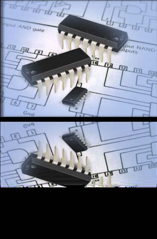
2 The Hashemite University Faculty of Engineering Department of Mechatronics Engineering Logic and Electronics Lab. Experiment 1 Objectives: In this experiment you will investigate the logic behavior of various IC gates such as: 7400 Quadruple 2 input NAND gates Quadruple 2 input NOR gates Hex inverters Quadruple 2 input AND gates Quadruple 2 input OR gates Quadruple 2 input XOR gates. To write Boolean functions in their standard Min and Max terms format. To simplify Boolean expressions using Karnaugh Map. Apparatus: This comprehensive digital analog training system is ideal for both analog and digital circuits and contains a wealth of equipment and features. The training system contains all the peripherals needed to support your logic circuit design. Components can be connected without soldering, by simply inserting them into the breadboard. Your circuit can then be powered by the internal power supplies, signals applied if needed from the function generator and monitored on the built-in test equipment and displays. Figure 1.1: Digital-Analog Training System Exp 1: Introduction to Combinational Logic 1 of 8
3 Theoretical Background: 1. Truth Tables A truth table is a table that describes the behavior of a logic gate. It lists the value of the output for every possible combination of the inputs and can be used to simplify the number of logic gates and level of nesting in an electronic circuit. 2. Simplification Logic functions can be complicated sometimes. In such cases we may use many tools to simplify them like: Boolean algebra theorems, De Morgan theorems or Karnaugh map. Boolean algebra theorems and De Morgan theorems will be the subject of this session while Karnaugh map will be the subject of the next session. 3. Boolean Algebra Theorems Table 2.1 shows Boolean algebra theorems. Associative law Distributive law Commutative law ( A. B). C = A. ( B. C) = ABC ( A + B) + C = A + ( B + C) = A + B + C ( B + C) = AB AC A. + ( B. C) = ( A + B)( A C) A + + A. B = B. A A + B = B + A AB = A. B Precedence A. B + C = ( AB) + C A + B. C = A + ( BC) Single variables theorems AA = A A + A = A A + A = 1 AA = 0 A = A Exp 1: Introduction to Combinational Logic 2 of 8
4 More two variables theorems Identity and Null operations A + AB = A A + AB = A + B A.1 = A A + 1 = 1 A + 0 = A A.0 = 0 1 = 0 0 = 1 Table 2.1: Boolean algebra theorems. Example 1.1 shows how to use Boolean algebra theorems in simplifying functions. Example 1.1: A(X,Y,Z) = (X + Y).(X' + Y) = XX'+XY+X'Y+YY = 0+Y(X+X)+Y = Y 4. De Morgan's Theorems The most important logic theorems for digital electronics are De Morgan's Theorems. These theorems state that any logical binary expression remains unchanged by applying all the following steps: Change all variables to their complements. Change all AND operations to ORs. Change all OR operations to ANDs. Take the complement of the entire expression. In Symbols, De Morgan's theorems are stated as follows: 1. ( A. B)' = A' + B' 2. ( A + B)' = A'. B' A practical operational way to look at De Morgan's Theorem is that the inversion bar of an expression may be broken at any point and the operation at that point replaced by its opposite (i.e., AND replaced by OR or vice versa). The following example shows the correct steps to apply De Morgan's theorems on a logic expression. Exp 1: Introduction to Combinational Logic 3 of 8
5 Example 1.2: A + BC A + ( B + C) Breaking shortest bar (AND changes to OR) A + B + C Applying associative property to remove parentheses A. B. C Breaking long bar in two places (ORs change to ANDs) A BC Applying the identity X = X 5. Sum of Products & Product of Sums Any Boolean expression can be simplified in many different ways resulting in different forms of the same Boolean function. All Boolean expressions, regardless of their forms, can be converted into one of two standard forms; the sum-of-product form and the product-of-sum forms. Standardization makes the evaluation, simplification and implementation of Boolean expression more systematic and easier. The Sum-of-Product (SOP): Writing functions in SOP form means that the inputs of each term are multiplied using AND function, then all terms are added together using OR function. The variables in each term are not necessarily all the variables of the function. For example, a SOP of F(A,B,C) may contain a term that contains only the variable A but not B nor C, in such case the term is not in its standard SOP form. Standard SOP term must contain all the function variables. From Boolean algebra thermos (X+X'=1), then if the term is multiplied by (X+X'), it becomes in the standard SOP form, but its value is not affected. Example 1.3: The following function is written in the SOP form: F(A,B,C)=A+BC'+A'BC The inputs to the function F are A, B and C. In each term the inputs are ANDed then all terms are ORed to form the function F. Note that the last term A'BC contains all the inputs of the function (A, B and C), so, this term is written in standard form. But the second term BC' is not in standard form because the input A does not exist, then multiply by (A'+A). The same is done for the remaining term as follows: F(A,B,C)=A(B+B')(C+C')+BC'(A+A')+A'BC F(A,B,C)=ABC+ABC'+AB'C+AB'C'+ ABC'+A'BC'+A'BC Exp 1: Introduction to Combinational Logic 4 of 8
6 From Boolean algebra, (A+A=A) then all similar terms in the equation will be reduced to one term. Now the function F becomes F(A,B,C)=ABC+ABC'+AB'C+AB'C'+ A'BC'+A'BC The Product-of-Sum (POS): Writing functions in POS form means that the inputs of each term are Added together using OR function then all terms are multiplied together using AND function. The variables in each term are not necessarily all the variables of the function. For example, a POS of F(A,B,C) may contain a term that contains only the variable A but not B nor C, in such case the term is not in its standard POS form. Standard POS term must contain all the function variables. From Boolean algebra thermos (X.X'=0), then if the term is added to (X.X'), it becomes in the standard POS form, but its value is not affected. Example 1.4: The following function is written in the POS form: F(A,B,C)=A.(B+C').(A'+B+C') The inputs to the function F are A, B and C. In each term the inputs are ORed then all terms are ANDed to form the function F. Note that the last term (A'+B+C') contains all the inputs of the function (A, B and C), so, this term is written in standard form. But the second term (B+C') is not in standard form because the input A does not exist, then add (A'.A). The same is done for the remaining term as follows: F(A,B,C)=[A+(B.B')+(C.C')].[(B+C')+(A.A')].(A'+B+C') F(A,B,C)=[(A+B+C).(A+B+C').(A+B'+C).(A+B'+C')].[(A+B+C').(A'+B+C')].(A'+B+C') From Boolean algebra, (A.A=A) then all similar terms in the equation will be reduced to one term. Now the function F becomes F(A,B,C)=(A+B+C).(A+B+C').(A+B'+C).(A+B'+C').(A'+B+C') 6. Minterms Writing a function in its minterm format is equivalent to writing the function in its standard SOP format such that the value of the function at these terms is 1. So that if we have the truth table relating the input variables to the function F, then we can determine which cases result in F=1 and write the minterm form of the function. Exp 1: Introduction to Combinational Logic 5 of 8
7 Example 1.5: Using the following truth table 1.2, write the function F in its minterm format The function F is equal to 1 in the highlighted cases, which are the cases of 0,2,6 and 7 or A'B'C', A'BC', ABC' and ABC respectively. The function F is written in minterm format as follows: F(A,B,C)= A'B'C'+A'BC'+ ABC'+ ABC Or F(A,B,C)= (0,2,6,7) 7. Maxterms Table 1.2 Writing a function in its maxterm format is equivalent to writing the function in its standard POS format such that the value of the function at these terms is 0. So that if we have the truth table relating the input variables to the function F, we can determine which cases result in F=0 and write the maxterm form of the function. Example 1.6: Using the truth table 1.2, write the function F in its maxterm format. A B C F The function F is equal to 0 in the un-highlighted cases above, which are the cases of 1,3,4 and 5 or (A+B+C'), (A+B'+C'), (A'+B+C) and (A'+B+C') respectively. The function F is written in maxterms as follows: F=(A+B+C').(A+B'+C').(A'+B+C). (A'+B+C') Or F(A,B,C)= Π(1,3,4,5) Note: From Example 1.3 and 1.4, the maxterm is the complement of the minterm. 8. Karnaugh Map The Karnaugh map (K-map) provides a systematic way of simplifying Boolean algebra expressions. This can be done without thoroughly searching the basic theorems of Boolean algebra. Instead all the possible combinations of the variables written in the standard form for POS (product of sums) or SOP (sums of products) are plotted in cells arranged in a rectangle or square. Adjacent cells share a redundant Boolean variable. The simplification of the original Boolean expression comes from grouping the logical one s (minterms) or 0 s (maxterms). This eliminates the redundant variable and simplifies the original Boolean expression. Exp 1: Introduction to Combinational Logic 6 of 8
8 The circulation must be done according to the following rules: 1. A group must contain either 1, 2, 4, 8, 16..cells. 2. Each cell in a group must be adjacent to one or more cells in the same group, but all cells do not have to be adjacent to each other. 3. Always include the most possible of 1 s in a group in accordance to rule (1). 4. Each 1 on the K-map must be included in at least one group. The 1 s in a group can be included in another group as long as the overlapping groups include non-common 1 s. Example 1.7 shows how to use the K-map to simplify functions. Example 1.7: Simply the following function using K-map F(A,B,C)=A'B+ABC'+B'C' In order to use the K-map the function should be written in its min or maxterms format. F(A,B,C)=A'BC+A'BC'+ABC'+AB'C'+A'B'C' F(A,B,C)= (0,2,3,4,6) To write the function as simplified SOP then circle the 1's in K-map From K-map, F(A,B,C)=C'+BA' F is written in maxterm as follows F(A,B,C)= Π(1,5,7) Exp 1: Introduction to Combinational Logic 7 of 8
9 To write the function as POS then circle the 0's in K-map From K-map, F(A,B,C)=(A'+C').(B+C') Procedure: 1- Ask your instructor to give you the digital logic IC's, after making your design on labwork sheet. 2- Insert the IC's in the digital training system breadboard, then referring to the datasheet connect your design 3- After being sure your circuit is connected correctly, turn on the digital training system power. Discussion and Analysis: 1- How many inputs, and outputs in your design? 2- If you decide to use maxterm instead of minterm simplification, is your design will be the same? explain. Exp 1: Introduction to Combinational Logic 8 of 8
10 The Hashemite University Faculty of Engineering Department of Mechatronics Engineering Logic and Electronics Lab. Experiment 2 Objectives: In this experiment you will be able to: Design a sequential logic circuit using D-Flip-flop. Implement the designed circuit. Design a sequential logic circuit using JK-Flip-Flop. Implement the designed circuit. Apparatus: This comprehensive digital analog training system is ideal for both analog and digital circuits and contains a wealth of equipment and features. The training system contains all the peripherals needed to support your logic circuit design. Components can be connected without soldering, by simply inserting them into the breadboard. Your circuit can then be powered by the internal power supplies, signals applied if needed from the function generator and monitored on the built-in test equipment and displays. Exp 2: Introduction to Sequential Logic 1 of 8
11 Theoretical Background: So far we have implemented digital circuits whose outputs depend only on its inputs in experiment 1,Such circuits are called combinational logic circuits and do not depend on the state of the output. Another type of digital circuits is presented in this session and called the sequential logic circuits. The next output Q+ (at time t+) of these circuits depends upon the present one Q (at time t) as well as upon the Boolean input variables. Sequential circuits have a memory of what has previously happened or in other words sequential circuits contain combinational circuits to which storage elements are connected to form a feedback path. The inputs for the sequential circuits together with the present state of the output determine the binary value of the next output. Memory Elements: The basic memory elements in sequential circuits are called latches and flip-flops. These devices -constructed from NAND and NOR gates- are bistable, this means that the latch or the flip-flop output can exist for an indefinite time in one of two stable states. By convention the output of a flip-flop is called Q. We set a flip-flop by changing "Q" to logical 1. We reset the flip-flop by changing "Q" to a logical 0. Flip-flops are heavily used for digital data storage and transfer and are commonly used in banks called "registers" for the storage of binary numerical data. There are four main types of flip-flops which are shown in Figure 2.1 Figure 2.1: Types of flip flops. Exp 2: Introduction to Sequential Logic 2 of 8
12 D Flip Flop: The D stands for "data"; this flip-flop stores the value presented at on the data line. It can be thought of as a basic memory cell. The D flip-flop tracks the input, making transitions that match those of the input D. The D flip-flop output "Q" tries to follow the input D but cannot make the required transitions unless it is enabled by a rising or falling edge of a clock. Table 2.1: D flip flop truth table. Input D Clock Next state Q Reset 1 1 Set And the characteristic equation for the D flip-flop is: D = Q( t) = Q + (2.1) The internal construction of D flip flop is shown in Figure 2.2. Figure 2.3 represents the time diagram of a D flip flop. Figure 2.2: Internal construction of D flips flop. Figure 2.3: Time diagram of D flip flops. Exp 2: Introduction to Sequential Logic 3 of 8
13 Logic Circuits Design Using D-Flip Flop. The best way to explain the procedure of designing using D flip flop is through an example. Example 2.1 Design using D flip flop a logic circuit that opens a door when a switch is turned on and the door is closed. And closes the door when the switch is turned off and the door is opened. The door is an output Y(Door closed=0) The switch is an input X (turned on=1) Solution: Step one: Derive circuit state diagram. The state diagram representing the problem in hand is shown in Figure 2.4. Figure 2.4: Example 2.1 state diagram. Step two: Create state table. The un-hashed columns in Table 2.2 represent the state table obtained from the state diagram. Input X Table 2.2: Example 2.1 state and excitation table. Current state Next state Q Q + D Y Exp 2: Introduction to Sequential Logic 4 of 8
14 Step three: Create circuit excitation table. This is shown by the hashed columns in Table 2.2. These columns are derived using Equation 2.1. Step four: Construct K-maps for the flip-flop input (D) and the output (Y). In this example the primary output Y is the same as the flip flop output Q which is the same as the input of the D flip flop, so only one K-map is enough to find the input D and the primary output Y. Observe Figure 2.5 and notice that the inputs of the k-map are the input X and the current state of the flip flop. According to the K-map above D=X Figure 2.5: Example 2.1 K-map. Then the input of the D flip flop will be connected directly to the switch X (only for this example) and it does not depend on the current state of the flip flop Q. Step five: Implement the logic circuit. The logic circuit for this application is shown in Figure 2.2. Figure 2.6: Logic circuit for Example 2.1. Exp 2: Introduction to Sequential Logic 5 of 8
15 Example 2.2 Design a logic circuit using D flip flop for the state diagram shown in Figure 2.7. Figure 2.7: State diagram for Example 2.2. Input Input Table 2.3: State and excitation table for Example 2.2. Current state Current state Next state Next state Output X Y Q1 Q2 Q1 + Q2 + F Exp 2: Introduction to Sequential Logic 6 of 8
16 Since D1= Q1 +, we can obtain the following K-map from Q1 + column. D1= Q1 + = Y'Q2 + XQ1'Q2' + XYQ2' + X'Y'Q1 Since D2= Q2 +, we can obtain the following K-map from Q2 + column. D2= Q2 + = XYQ1Q2' + X'Q1'Q2' + Y'Q1'Q2 + X'Y'Q2' The following K-map is obtained from the primary output F column. Exp 2: Introduction to Sequential Logic 7 of 8
17 F = XQ1'Q2 + XY'Q1' + Y'Q1'Q2 + X'YQ1'Q2' + X'Y'Q1Q2' The logic circuit for Q1 and Q2 are shown in Figure 2.8. The logic circuit of the primary output F is omitted for simplicity. Procedure: Figure 2.8: Logic circuit for Example Ask your instructor to give you the digital logic IC's, after making your design on labwork sheet. 2- Insert the IC's in the digital training system breadboard, then referring to the datasheet connect your design 3- After being sure your circuit is connected correctly, turn on the digital training system power. Discussion and Analysis: 1- How many inputs you need in your design. 2- If you design your logic circuit using D-flip flop, change your design to use JK flip flop. Is it easier than using D-flip flop? Exp 2: Introduction to Sequential Logic 8 of 8
18 The Hashemite University Faculty of Engineering Department of Mechatronics Engineering Logic and Electronics Lab. Experiment 3 Objectives: To use decoders to implement logic functions. To implement decoders using 74LS138 and 74LS139 ICs. To design digital counter circuits using JK-Flip-Flop. To implement counter using 74LS193 IC. Apparatus: This comprehensive digital analog training system is ideal for both analog and digital circuits and contains a wealth of equipment and features. The training system contains all the peripherals needed to support your logic circuit design. Components can be connected without soldering, by simply inserting them into the breadboard. Your circuit can then be powered by the internal power supplies, signals applied if needed from the function generator and monitored on the built-in test equipment and displays. Exp 3: Decoders & Counters 1 of 6
19 Theoretical Background: Decoders Discrete quantities of information are represented in digital system with binary codes. A binary code of N bits is capable of representing up to 2 N distinct combinations. A decoder is a digital circuit that detects the presence of a specified combination of bits (code) on its input and indicates the presence of that code by a specified output level. In its general form, a decoder has n input lines to handle N bits and from one to 2 N output lines to indicate the presence of one or more N-bit combinations. Consider a 2*4 decoder, it has 2 inputs and 4 output lines. The truth table for a 2*4 decoder is shown in Table 3.1. Inputs Table 3.1: Truth table of 2*4 decoder. Outputs A B D0 D1 D2 D Each combination of inputs (A & B) activates only one output line. From the truth table, D0=A'.B' D1=A'.B D2=A.B' D3=A.B Because the active output in each case is indicated by a HIGH signal (one), this type of decoders is called active HIGH decoders. On the other hand, if the active output is indicated by a LOW signal (zero), the decoder is called active LOW decoders. The decoder circuit is shown in Figure 3.1 and its symbol is shown in Figure 3.2. Figure 3.1: 2*4 decoder logic circuit. Exp 3: decoders & Counters 2 of 6
20 Figure 3.2: 2*4 decoder circuit symbol. An active LOW decoder IC of N inputs has 2 N output, but can be used to generate a single active HIGH output by using NAND as illustrated by the following example: Example 3.1: Design a logic circuit using an active LOW 2*4 decoder, such that: F(A,B)= (1,2) where F is an active HIGH function. Solution: The function F is HIGH when the input combination is AB' or A'B. In other words, when the output lines D1 or D2 (of the active LOW decoder) are LOW. The logic circuit needed to build the function F is shown by Figure 3.3. Figure 3.3: Logic circuit needed to solve Example 3.1. Counter Circuits for counting events are frequently used in computers and other digital systems. Since a counter circuit must remember its past states, it has to possess memory. Flip-flops are introduced and connected to make a counter. The number of flip-flops used and how they are connected determine the number of states and the sequence of the states that the counter goes through in each complete cycle. Counters can be classified into two broad categories: a. Synchronous counters b. Asynchronous counters Exp 3: decoders & Counters 3 of 6
21 a- Synchronous Counters: In synchronous counter all clocks of flip-flops are connected to the same clock signal. Thus, all flip-flop outputs change state at precisely the same moment. Table 3.2 shows the states of a 2-bit counter. Each state is an increment to its previous state by 1, which means that the counter is an up counter. It is clear from the table that the first flip-flop (FF0) toggles at the clock edge (either rising or falling), according to this, this part of the counter is implemented using T flip-flop and its input is always at high logic. The second flip-flop (FF1) toggles if the output of FF0 is 1. Then this part of the counter is also implemented with T flip-flop but with its input connected to the output of the previous flip-flop. Table 3.2: 2-bit counter. Q1 Q Figure 3.4: 2-bit synchronous counter. Example 3.2 Design a logic circuit that counts from 0 to 4 then back to 0 only if an input signal is 1. Use synchronous counter. Solution: Step one: Figure 8.5 shows the state diagram. Figure 3.5: Example 3.2 state diagram Step two and three: The state and excitation tables are shown in table 3.3. Exp 3: decoders & Counters 4 of 6
22 Table 3.3: State and excitation tables of Example 3.2. Current state Input Next state Flip flop 1 Flip flop 0 Q1 Q0 U Q1 + Q0 + J1 K1 J0 K X 0 X X 1 X X X X X X 0 0 X X 0 1 X X 0 X X 1 X 1 Step four: Construct K-maps for each flip-flop inputs (J and K) J0=U Figure 3.6: K-map for J0 in Example 3.2. Figure 3.7: K-map for K0 in Example 3.2. K0= U Notice that even though the implementation is with JK flip-flop the result is that K0=J0 then it is a T flip-flop Exp 3: decoders & Counters 5 of 6
23 Figure 3.8: K-map for J1=K1 in Example 3.2. J1=K1=Q0.U Step five: The logic circuit is implemented in Figure 3.9. Figure 3.9: The logic circuit for Example 3.2 Procedure: For synchronous counter, the design procedure is the same procedure of designing using flipflops, starting from the state diagram and ending with the logic circuit. Discussion and Analysis: Design a 4-bit logic circuit that counts from 2 to 7, only if an input signal is 1. Use synchronous counter. Hints: you have to use decoder to stop counting at 7. Exp 3: decoders & Counters 6 of 6
24 The Hashemite University Faculty of Engineering Department of Mechatronics Engineering Logic and Electronics Lab. Experiment 4 Objectives: In this experiment you are expected: To be familiar with basic properties of diodes, Zener diodes and LED. To study the characteristics of the diode by investigating the I-V curve. To study the characteristics of the Zener diode by investigating the I-V curve. To differentiate between regular diode and Zener diode properties. Apparatus: Theoretical Background: A diode is a semiconductor device consists of single pn-junction with nonlinear i-v characteristics. Diode permits current conduction in only one direction; from the anode (the positive terminal) to the cathode (the negative terminal) forming one way switch see figure 1. Its operation falls in one of three regions: 1. Forward biased. 2. Reverse biased. 3. Reverse breakdown (failure). Zener diode is a special type of diodes designed to operate in the reverse breakdown region, where it maintain a constant voltage drop across its terminals. LEDs -or Light Emitting Diodes- are another type of diodes that emits light when forward biased. The color emitting from each diode depends on the materials of the pn-junction. Exp 4: Diode Types and Characteristics 1 of 6
25 Procedure: Part1: Forward and Reverse Voltages of Diodes Use the DMM to measure the voltages in table 4.1. Set the DMM to the "diode testing" option. Technical hints: Anode and cathode of diodes are shown in figure 4.1 To measure the forward voltage place the positive lead of the DMM on the anode To measure the reverse voltage place the positive lead of the DMM on the cathode Figure 4.1 Table 4.1 Diode type Forward voltage Reverse voltage Observation Regular diode Zener diode LED (color1) LED (color2) Exp 4: Diode Types and Characteristics 2 of 6
26 Part2: Diode Characteristics a. Forward biasing 1. Connect the circuit in figure Measure V out and I D and fill in table 4.2. Figure 4.2 Table 4.2: Vs (V) 0 Forward voltage V out (V) Forward current I D (A) Exp 4: Diode Types and Characteristics 3 of 6
27 b. Reverse biasing 1. Connect the circuit in figure Measure V out and I D and fill in table 4.3. Figure 4.3 Table 4.3 Vs (V) 1 Reverse voltage V out (V) Reverse current I s (A) Exp 4: Diode Types and Characteristics 4 of 6
28 c. Characteristic curve Connect the circuit in figure 4.4. Set the oscilloscope on the (XY measurement). Observe the result, and write down the values of : V D = I s = Figure 4.4 Technical hints: R2 must be a multiple of 10KΩ for current scaling Invert channel 2 of the oscilloscope to obtain a positive reading of the current Part3: Zener Characteristics Repeat Part 2 but first replace all diodes in the circuits with Zener diodes then fill in the following tables: a. Forward biasing Vs (V) 0 Table 4.4: Forward voltage V out (V) Forward current I D (A) Exp 4: Diode Types and Characteristics 5 of 6
29 b. Reverse biasing Table 1.5 Vs (V) 1 Reverse voltage V out (V) Reverse current I s (A) c. Characteristic curve V z = I s = Discussion and Analysis: Part1: Forward and Reverse Voltages of Diodes 1. Fill in table 1.1 with your observations. Part2: Diode Characteristics 2. In table 1.2, the output voltage reached a constant value. What is this value? And what does it represent? 3. What is the purpose of using R1 in the circuit of figure1.1? 4. Sketch the result you obtain from the circuit in figure 1.4. On your sketch, show the values of V D and I s. 5. Based on your result; dose ohm's law apply to the diodes? 6. What would it cost to obtain the breakdown voltage of a diode? Part3: Zener Characteristics 7. In table 1.4, the output voltage reached a constant value. What is this value? And what does it represent? 8. Does the behavior of the Zener diode differ from that of a regular diode in the forward biased region? 9. Compare the results you obtained in table 1.5 (reverse biased Zener diode) to the results in table 1.3 (reverse biased regular diode). 10. Sketch the result you obtain from the circuit in figure 1.4 for the Zener diode. On your sketch, show the values of V D,V Z and I s. Exp 4: Diode Types and Characteristics 6 of 6
30 The Hashemite University Faculty of Engineering Department of Mechatronics Engineering Logic and Electronics Lab. Experiment 5 Objectives: In this experiment you are expected: To implement clipper circuits. To implement clamper circuits. To implement two types of diode rectification circuits half-wave and full-wave rectifiers. To implement a voltage regulation circuit using Zener diodes. Apparatus: Theoretical Background: Important applications of diode are wave-shaping circuits that either limit portions of a signal (clipper) or shift the dc voltage level (clamper). Clipper circuits are used to eliminate portion of a signal that are above or below a specified level. Clamper circuits shifts the entire signal voltage by dc level. The output is an exact replica of the input waveform, but with different dc level. A common application of diode circuits are rectifiers. A rectifier is an electrical device that converts alternating current (AC), which periodically reverses direction, to direct current (DC), which flows in only one direction. Exp 5: Diodes Applications 1 of 9
31 Rectifier can be constructed using diode circuits and there are two types: 1. Half-wave rectifier. 2. Full-wave rectifier. Another application of diodes circuits are voltage regulators. Voltage regulator is a circuit used to maintain a steady voltage across a load which otherwise may vary according to the change of the input voltage (line regulation) or the change of the load impedance (load regulation). Procedure: Part1: Clippers 1. Connect the circuit in figure5.1. Figure Consult your lab supervisor to get the correct sitting of the sinwave and the value of the resistors. 3. Plot the input and output signals on the oscilloscope monitor. (make sure that both channel has the same ground) 4. Do the needed measurements to complete table 5.1 Table 5.1 Experimental Theoretical V max V min V max V min Exp 5: Diodes Applications 2 of 9
32 Part2: Clampers 1. Connect the circuit in figure5.2. Figure 5.2 Technical hints: Make sure in clamper circuit that the positive terminal of the electrolytic capacitor is connected to the cathode of the diode, or the negative terminal of the electrolytic capacitor is connected to the anode of the diode. The only design constraint in clamper circuit is that the period 2πRC be five times larger than the period of the input waveform. 2. Consult your lab supervisor to get the correct sitting of the sinwave and the value of the resistors. 3. Plot the input and output signals on the oscilloscope monitor. (make sure that both channel has the same ground) 4. Change the input signal into a squarewave. Consult your supervisor. 5. Do the needed measurements to complete table 5.2. Input 1 sinewave Output 1 Table 5.2 V max V min waveform Input 2 Squarewave Output 2 Part3: Half-Wave Rectifiers a. Unfiltered half-wave rectifier 5. Connect the circuit in figure5.3. Exp 5: Diodes Applications 3 of 9
33 Figure Consult your lab supervisor to get the correct sitting of the function generator and the value of R. 7. Plot the input and output signals on the oscilloscope monitor. (make sure that both channel has the same ground) b. Filtered half-wave rectifier 1. For the circuit in figure 5.3, connect a capacitor in parallel with the resistor to get a circuit similar to figure 5.4. Figure 5.4 Technical hints: Make sure to connect the capacitor with the proper polarity. See figure 5.5 Figure 5.5 Exp 5: Diodes Applications 4 of 9
34 2. Plot the input and output signals on the oscilloscope monitor. (make sure that both channel has the same ground) 3. Use the oscilloscope to measure the ripple voltage V r =. Part4: Full-Wave Rectifier 6. Connect the circuit in figure5.6. Figure 5.6 Technical hints: In this case the output is a deference voltage and is measured as illustrated in the next steps. 7. Connect the oscilloscope as shown in figure 5.6 then invert channel Add the signal in both channels (by this you subtracted channel 2 from channel 1 and founded the deference voltage). 9. Observe the result. 10. Measure the ripple voltage V r1 =. 11. Increase the capacitor value and measure the ripple voltage V r2 =. Part5: Voltage Regulators a. Line regulation. 1. Connect the circuit in figure 5.7 use the values in table 5.3 Figure 5.7 Exp 5: Diodes Applications 5 of 9
35 2. Measure V L and V 1 and fill in table 5.3 Table 5.3 measured V 1 Vs (V) V L (V) (V) calculated I s I Z I L RL=2.2KΩ R1=220Ω VR= b. Load regulation 1. For the circuit in figure 5.7 use the values in table Measure V L and V 1 and fill in table 5.4. Table 5.4 measured calculated R L (Ω) V L (V) V 1 (V) I s I Z I L 1.0K V s =6V R1=220Ω VR= Exp 5: Diodes Applications 6 of 9
36 Discussion and Analysis: Part1: Clipper 1. Sketch the output waveform of the circuit in figure Assume that the diode is ideal then complete table Is there a difference between the experimental and theoretical values? Give one good reason for that. 4. Sketch the output waveform of the circuit in figure5.1 if the diode polarity is inverted. 5. Sketch the output wave form of the circuit in figure5.8. Is this circuit considered as a clipper? Figure 5.8 Part2: Clamper 6. Include table 5.2 with your report showing the waveforms of the signals. 7. Sketch the output waveform of the circuit in figure5.9? Figure Construct a clamper circuit to obtain the waveform in figure Assume that Vγ=0.8 Figure 5.10 Exp 5: Diodes Applications 7 of 9
37 Part3: Half-Wave Rectifier 1. Sketch the output waveform of the circuit in figure Assume that the diode is ideal then complete table5.2. Show the equations you used. 3. Is there a difference between the experimental and theoretical values of V max. give one good reason for that. 4. Sketch the output waveform of the circuit in figure5.3 if the diode polarity is inverted. 5. Sketch the output waveform of the circuit in figure Calculate the output average voltage V ave = V p /π-(v γ /2). 7. Calculate the ripple percentage r=v r /V ave. 8. Sketch the output wave form of the circuit in figure5.11. Is this circuit considered as a rectifier? Figure 5.11 Part4: Full-Wave Rectifier 9. Sketch the output waveform of the circuit in figure 5.6? 10. What is the effect of increasing the capacitor value on the ripple voltage? Which capacitor is better to use? Part5: Voltage Regulators 11. Calculate I s, I L, I Z and fill in table Calculate the line regulation VR= ΔV out /ΔV in *100% 13. Calculate I s, I L, I Z and fill in table Calculate the load regulation VR= (V nl -V fl )/V fl *100% 15. What is the purpose of using R 1? 16. For the circuit in figure 2.6, the load is 0.9A and must be operated at a constant voltage in the range of (8-9V),) chose a suitable Zener diode then calculate the minimum value of R 1. Include the datasheet of the Zener diode you've chosen with your report. Figure 5.12 Exp 5: Diodes Applications 8 of 9
38 Exp 5: Diodes Applications 9 of 9
39 The Hashemite University Faculty of Engineering Department of Mechatronics Engineering Logic and Electronics Lab. Experiment 6 Objectives: In this experiment you are expected: To experimentally distinguish between the types of Bipolar Junction Transistor (BJT) npn and pnp. Determine the terminals and material of a npn BJT using DMM. To experimentally obtain the characteristics of the npn BJT Apparatus: Theoretical Background: The bipolar junction transistor (BJT) contains two pn junctions, so it has three terminals. The basic transistor principle is that the voltage between two terminals controls the current through the third terminal. BJT has three regions of operation; Active region, Saturation region and Cutoff region. If a BJT is to be used as an amplifier it must be biased to operate in the Active region, where the output current is proportional to the input voltage. If the BJT is to be used as electrical switch (ON-OFF control circuits); it is biased to operate in the Saturation region (ON state, where the current is constant) or in the Cutoff region (OFF state where the current is zero). Exp 6: BJT 1 of 4
 and assign its terminals (base 'B', collector 'C' and emitter 'E'). Figure 6.1 Figure 6.2 1.")
40 Procedure: Part1: Transistor Testing Figure 6.1 shows the electrical symbol of pnp and npn transistors and figure 6.2 shows a physical transistor. Follow the next steps to find the type of the transistor (npn or pnp) and assign its terminals (base 'B', collector 'C' and emitter 'E'). Figure 6.1 Figure Write down the number written on the back of your transistor. 2. Label the terminal of the transistor as in figure Set the selector of the DMM on the diode option. 4. Connect the positive and negative leads of the DMM to the BJT terminals as specified in table 6.1. Record the DMM reading each time you test the terminals. Table 6.1 Step Positive terminal of Negative terminal of the DMM connected to: the DMM connected to: DMM reading 1 Terminal 1 Terminal 2 2 Terminal 2 Terminal 1 3 Terminal 1 Terminal 3 4 Terminal 3 Terminal 1 5 Terminal 2 Terminal 3 6 Terminal 3 Terminal 2 Observation : npn/pnp Note that the emitter-base voltage is slightly higher than the collector-base voltage. Exp 6: BJT 2 of 4
41 Part2: Transistor Parameters and DC Load Line 1. Connect the circuit in figure 6.3. Figure Measure the values in table 6.2 Table 6.2 parameter measured calculated Error% V C V B V E I CQ I BQ I EQ V CEQ V BEQ Calculate the dc current gain β dc : Part3: Transistor Switch 1. Connect the circuit in figure 6.4. Figure 6.4 Exp 6: BJT 3 of 4
42 2. Consult your lab supervisor to get the correct values of the resistors. Warning: both switches should NOT be closed at the same time. 3. Close the switches as illustrated in table 6.3 and do the needed measurement Table 6.3 Switches state parameter x open y closed y open x closed V C V B V E LED state On/off Transistor region of operation Discussion and Analysis: Part1: Transistor Testing 1. Based on the data in table 6.1 what is the type of the transistor? 2. Assign the emitter, collector and base of the transistor based on the measurements in table 6.1. Part2: Transistor Parameters and DC Load Line 1. Analyze the circuit in figure 6.3 and fill the values you calculated in table 6.2. Include table 6.2 with your report. 2. Calculate the percentage error in each parameter. 3. Calculate the current gain βdc= IC/ IB 4. Write down the load line equation. VCE = f(ic). 5. Plot the load line and assign the measured Q-point on it Exp 6: BJT 4 of 4

43 The Hashemite University Faculty of Engineering Department of Mechatronics Engineering Logic and Electronics Lab. Experiment 7 Objectives: In this experiment you are expected: To experimentally deal with OP-Amps. Apparatus: Theoretical Background: An operational amplifier (op-amp) is a DC-coupled high-gain electronic voltage amplifier with a differential input and, usually, a single-ended output. An op-amp produces an output voltage that is typically hundreds of thousands times larger than the voltage difference between its input terminals. The circuit symbol for an op-amp is shown by figure 7.1, where, V+: non-inverting input V-: inverting input Vout: output Vs+: positive power supply Vs-: negative power supply Exp 7: Op-Amp 1 of 5
44 Figure 7.1 Ideal operational amplifier has the following specifications: 1. Infinite input resistance. 2. Zero output resistance. 3. Infinite common mode rejection ratio (CMRR). 4. Zero input current and input voltage offsets. Ideal op-amp does not really exist. This will cause some practical issues. Technical hints: The positive and negative power supply must be connected properly. See the datasheet of the IC. For a zero input voltage, the output of a real op-amp is not zero. The solution to this problems is to null the amplifier to compensate for this offsets. See figure 7.2. Figure 7.2 Op-amp can be implemented in circuits in different configuration to perform different tasks such as: 1. Inverting amplifier. 2. Non-inverting amplifier 3. Summing amplifier. 4. Differential amplifier. 5. Instrumentation amplifier 6. Integration amplifier Exp 7: Op-Amp 2 of 5
45 Procedure: Part1: Op-amp Nulling 1. Implement the circuit shown in Figure Switch on the power supplies. 3. While Vin=0 V and the switches are open, measure the output voltage V out =. 4. While Vin=0 V, adjust the potentiometer till the output voltage equals 0V. 5. Note that this procedure must be done each time you implement an op-amp circuit. Figure 7.3 \ Part2: Inverting Amplifier 1. Implement the circuit shown in figure Consult your lab supervisor to get the values of the resistors. 3. Switch on the power supplies. 4. While V in =0 V, Adjust the potentiometer to null the op-amp. 5. Adjust the value of V in and fill in table 7.1 Figure 7.4 Exp 7: Op-Amp 3 of 5
46 Part3: Summation Amplifier 1. Implement the circuit shown in figure Consult your lab supervisor to get the values of the resistors. 3. Switch on the power supplies. 4. While V in =0 V, Adjust the potentiometer to null the op-amp. 5. Adjust the value of V in and fill in table 7.1 Figure 7.5 Part4: Difference Amplifier 1. Implement the circuit shown in figure Consult your lab supervisor to get the values of the resistors. 3. Switch on the power supplies. 4. While V in =0 V, Adjust the potentiometer to null the op-amp. 5. Adjust the value of V in and fill in table 7.1 Figure 7.6 Exp 7: Op-Amp 4 of 5
47 Table 7.1 V in (V) V out Inverting amplifier Summation amplifier Difference amplifier Discussion and Analysis: Part1: Op-amp Nulling 1. If the op-amp is ideal what is the value of V out while the switch is open? Part2: Inverting Amplifier 2. Plot the output voltage of the inverting amplifier versus the input voltage. 3. From your plot, find the slope of the curve. What does the slope represent? 4. Calculate the gain of the inverting amplifier and compare it with the gain you obtained experimentally. Part3: Summation Amplifier 5. On the same plot in step 2, plot the output voltage of the summing amplifier versus the input voltage. 6. From your plot, find the slope of the curve. What does the slope represent? Part4: Difference Amplifier 7. Plot the output voltage of the deference amplifier versus the input voltage. Calculate the slope. 8. In all circuits of this experiment, what happens to the output when the input voltage is more than 6V? Explain. Exp 7: Op-Amp 5 of 5

48 The Hashemite University Faculty of Engineering Department of Mechatronics Engineering Logic and Electronics Lab. Experiment 8 Objectives: In this experiment you are expected: To experimentally deal with SCR. To experimentally deal with TRIAC. Apparatus: Theoretical Background: The Thyristor is a multi-layer semiconductor device that is used mainly as AC switches in AC power circuits, it is similar to the transistor. It requires a gate signal to turn it ON, the controlled part of the name and once ON it behaves like a rectifying diode, the rectifier part of the name. In fact the circuit symbol for the thyristor suggests that this device acts like a controlled rectifying diode. Examples on Thyristors: 1. SCR (Silicon Controlled Rectifier) Thyristor. See Figure Diac. See Figure Triac. See Figure 8.3. Exp 8: Thyristors 1 of 3
49 SCR (silicon controlled rectifier): is a special type of diode that only allows current to flow when a control voltage is applied to it's gate terminal. Although this appears to be nothing more than a voltage controlled switch the following should be noted: In the presence of forward current (i.e. after the thyristor is turned on by a suitable gate voltage) it will not turn off even after the gate voltage has been removed. The thyristor will only turn off when the forward current drops to zero. In a DC (Direct current) circuit this makes the device almost useless except in certain particular safety (crowbar) protection applications. Diac (Diode Alternating Current) is a full-wave or bi-directional semiconductor switch that can be turned on in both forward and reverse polarities, it is widely used to assist even triggering of a TRIAC when used in AC switches. DIACs are mainly used in dimmer applications and also in starter circuits for florescent lamps. The TRIAC (Triode for Alternating Current) is a three terminal semiconductor device for controlling current, it is effectively a development of the SCR or thyristor, but unlike the thyristor which is only able to conduct in one direction, the TRIAC is a bidirectional device. Procedure: Part1: SCR (BT151) 1. Construct the circuit shown in Figure Switch on the power supply. 3. Increase V1 slowly from 0V to 12 V 4. Keep the power supply on (12V),and Close the switch J1 while the gate voltage is zero,what happen? 5. Increase the gate voltage slowly till the led will be on. What is the Voltage at this moment? Calculate the needed current? 6. Open the switch J1, Write your observation. 7. How can you reset the thyristor? 8. Decrease the Supply voltage from 12V slowly, what is the minimum voltage for working. Figure 8.4 Exp 8: Thyristors 2 of 3
50 Discussion and Analysis: 1- In step 3 (procedure), Is the LED turn on?, why. 2- while you Increasing the gate voltage slowly,what is the Voltage at switching? Calculate the needed current? Exp 8: Thyristors 3 of 3
ELECTRONIC CIRCUITS. Time: Three Hours Maximum Marks: 100
 EC 40 MODEL TEST PAPER - 1 ELECTRONIC CIRCUITS Time: Three Hours Maximum Marks: 100 Answer five questions, taking ANY TWO from Group A, any two from Group B and all from Group C. All parts of a question
Analog Electronic Circuits Lab-manual
 2014 Analog Electronic Circuits Lab-manual Prof. Dr Tahir Izhar University of Engineering & Technology LAHORE 1/09/2014 Contents Experiment-1:...4 Learning to use the multimeter for checking and indentifying
Chapter 3 Digital Logic Structures
 Chapter 3 Digital Logic Structures Transistor: Building Block of Computers Microprocessors contain millions of transistors Intel Pentium 4 (2): 48 million IBM PowerPC 75FX (22): 38 million IBM/Apple PowerPC
Fan in: The number of inputs of a logic gate can handle.
 Subject Code: 17333 Model Answer Page 1/ 29 Important Instructions to examiners: 1) The answers should be examined by key words and not as word-to-word as given in the model answer scheme. 2) The model
Number system: the system used to count discrete units is called number. Decimal system: the number system that contains 10 distinguished
 Number system: the system used to count discrete units is called number system Decimal system: the number system that contains 10 distinguished symbols that is 0-9 or digits is called decimal system. As
R.B.V.R.R. WOMEN S COLLEGE (AUTONOMOUS) Narayanaguda, Hyderabad. ELECTRONIC PRINCIPLES AND APPLICATIONS
 Narayanaguda, Hyderabad. ELECTRONIC PRINCIPLES AND APPLICATIONS") R.B.V.R.R. WOMEN S COLLEGE (AUTONOMOUS) Narayanaguda, Hyderabad. DEPARTMENT OF PHYSICS QUESTION BANK FOR SEMESTER V PHYSICS PAPER VI (A) ELECTRONIC PRINCIPLES AND APPLICATIONS UNIT I: SEMICONDUCTOR DEVICES
R.B.V.R.R. WOMEN S COLLEGE (AUTONOMOUS) Narayanaguda, Hyderabad. DEPARTMENT OF PHYSICS QUESTION BANK FOR SEMESTER V PHYSICS PAPER VI (A) ELECTRONIC PRINCIPLES AND APPLICATIONS UNIT I: SEMICONDUCTOR DEVICES
OBJECTIVE TYPE QUESTIONS
 OBJECTIVE TYPE QUESTIONS Q.1 The breakdown mechanism in a lightly doped p-n junction under reverse biased condition is called (A) avalanche breakdown. (B) zener breakdown. (C) breakdown by tunnelling.
B.E. SEMESTER III (ELECTRICAL) SUBJECT CODE: X30902 Subject Name: Analog & Digital Electronics
 SUBJECT CODE: X30902 Subject Name: Analog & Digital Electronics") B.E. SEMESTER III (ELECTRICAL) SUBJECT CODE: X30902 Subject Name: Analog & Digital Electronics Sr. No. Date TITLE To From Marks Sign 1 To verify the application of op-amp as an Inverting Amplifier 2 To
B.E. SEMESTER III (ELECTRICAL) SUBJECT CODE: X30902 Subject Name: Analog & Digital Electronics Sr. No. Date TITLE To From Marks Sign 1 To verify the application of op-amp as an Inverting Amplifier 2 To
PESIT BANGALORE SOUTH CAMPUS BASIC ELECTRONICS
 PESIT BANGALORE SOUTH CAMPUS QUESTION BANK BASIC ELECTRONICS Sub Code: 17ELN15 / 17ELN25 IA Marks: 20 Hrs/ Week: 04 Exam Marks: 80 Total Hours: 50 Exam Hours: 03 Name of Faculty: Mr. Udoshi Basavaraj Module
Electronics. Digital Electronics
 Electronics Digital Electronics Introduction Unlike a linear, or analogue circuit which contains signals that are constantly changing from one value to another, such as amplitude or frequency, digital
Dev Bhoomi Institute Of Technology Department of Electronics and Communication Engineering PRACTICAL INSTRUCTION SHEET
 Dev Bhoomi Institute Of Technology Department of Electronics and Communication Engineering PRACTICAL INSTRUCTION SHEET LABORATORY MANUAL EXPERIMENT NO. ISSUE NO. : ISSUE DATE: REV. NO. : REV. DATE : PAGE:
R & D Electronics DIGITAL IC TRAINER. Model : DE-150. Feature: Object: Specification:
 DIGITAL IC TRAINER Model : DE-150 Object: To Study the Operation of Digital Logic ICs TTL and CMOS. To Study the All Gates, Flip-Flops, Counters etc. To Study the both the basic and advance digital electronics
GOVERNMENT OF KARNATAKA KARNATAKA STATE PRE-UNIVERSITY EDUCATION EXAMINATION BOARD II YEAR PUC EXAMINATION JULY-2012 SCHEME OF VALUATION
 GOVERNMENT OF KARNATAKA KARNATAKA STATE PRE-UNIVERSITY EDUCATION EXAMINATION BOARD II YEAR PUC EXAMINATION JULY-0 SCHEME OF VALUATION Subject Code: 40 Subject: PART - A 0. Which region of the transistor
HIGH LOW Astable multivibrators HIGH LOW 1:1
 1. Multivibrators A multivibrator circuit oscillates between a HIGH state and a LOW state producing a continuous output. Astable multivibrators generally have an even 50% duty cycle, that is that 50% of
Introduction to Electronics. Dr. Lynn Fuller
 ROCHESTER INSTITUTE OF TECHNOLOGY MICROELECTRONIC ENGINEERING Introduction to Electronics Dr. Lynn Fuller Webpage: http://www.rit.edu/~lffeee 82 Lomb Memorial Drive Rochester, NY 14623-5604 Tel (585) 475-2035
Objective: To study and verify the functionality of a) PN junction diode in forward bias. Sl.No. Name Quantity Name Quantity 1 Diode
 PN junction diode in forward bias. Sl.No. Name Quantity Name Quantity 1 Diode") Experiment No: 1 Diode Characteristics Objective: To study and verify the functionality of a) PN junction diode in forward bias Components/ Equipments Required: b) Point-Contact diode in reverse bias Components
Experiment No: 1 Diode Characteristics Objective: To study and verify the functionality of a) PN junction diode in forward bias Components/ Equipments Required: b) Point-Contact diode in reverse bias Components
Experiment No. 1 Half Wave Rectifier using R-Triggering
 Experiment No. 1 Half Wave Rectifier using R-Triggering Pre-Lab Reading: Power Electronics: Circuits, Devices and Applications, by M. H. Rashid, 3e. Objectives: To analyze resistive firing/triggering of
Subject: Analog and Digital Electronics Code:15CS32
 Subject: Analog and Digital Electronics Code:15CS32 Syllabus: The Basic Gates : Review of Basic Logic gates, Positive and Negative Logic, Introduction to HDL. Combinational Logic Circuits:Sum-of-Products
ELT 215 Operational Amplifiers (LECTURE) Chapter 5
 Chapter 5") CHAPTER 5 Nonlinear Signal Processing Circuits INTRODUCTION ELT 215 Operational Amplifiers (LECTURE) In this chapter, we shall present several nonlinear circuits using op-amps, which include those situations
CHAPTER 5 Nonlinear Signal Processing Circuits INTRODUCTION ELT 215 Operational Amplifiers (LECTURE) In this chapter, we shall present several nonlinear circuits using op-amps, which include those situations
Preface... iii. Chapter 1: Diodes and Circuits... 1
 Table of Contents Preface... iii Chapter 1: Diodes and Circuits... 1 1.1 Introduction... 1 1.2 Structure of an Atom... 2 1.3 Classification of Solid Materials on the Basis of Conductivity... 2 1.4 Atomic
Digital Electronics Course Objectives
 Digital Electronics Course Objectives In this course, we learning is reported using Standards Referenced Reporting (SRR). SRR seeks to provide students with grades that are consistent, are accurate, and
Electronics Lab. (EE21338)
") Princess Sumaya University for Technology The King Abdullah II School for Engineering Electrical Engineering Department Electronics Lab. (EE21338) Prepared By: Eng. Eyad Al-Kouz October, 2012 Table of
Princess Sumaya University for Technology The King Abdullah II School for Engineering Electrical Engineering Department Electronics Lab. (EE21338) Prepared By: Eng. Eyad Al-Kouz October, 2012 Table of
Unit/Standard Number. LEA Task # Alignment
 1 Secondary Competency Task List 100 SAFETY 101 Demonstrate an understanding of State and School safety regulations. 102 Practice safety techniques for electronics work. 103 Demonstrate an understanding
Revised April Unit/Standard Number. Proficiency Level Achieved: (X) Indicates Competency Achieved to Industry Proficiency Level
 Indicates Competency Achieved to Industry Proficiency Level") Unit/Standard Number Electrical, Electronic and Communications Engineering Technology/Technician CIP 15.0303 Task Grid Secondary Competency Task List 100 SAFETY 101 Demonstrate an understanding of state,
Unit/Standard Number Electrical, Electronic and Communications Engineering Technology/Technician CIP 15.0303 Task Grid Secondary Competency Task List 100 SAFETY 101 Demonstrate an understanding of state,
LABORATORY EXPERIMENT. Infrared Transmitter/Receiver
 LABORATORY EXPERIMENT Infrared Transmitter/Receiver (Note to Teaching Assistant: The week before this experiment is performed, place students into groups of two and assign each group a specific frequency
Lab 2 Revisited Exercise
 Lab 2 Revisited Exercise +15V 100k 1K 2N2222 Wire up led display Note the ground leads LED orientation 6.091 IAP 2008 Lecture 3 1 Comparator, Oscillator +5 +15 1k 2 V- 7 6 Vin 3 V+ 4 V o Notice that power
COMBINATIONAL and SEQUENTIAL LOGIC CIRCUITS Hardware implementation and software design
 PH-315 COMINATIONAL and SEUENTIAL LOGIC CIRCUITS Hardware implementation and software design A La Rosa I PURPOSE: To familiarize with combinational and sequential logic circuits Combinational circuits
IFB270 Advanced Electronic Circuits
 IFB270 Advanced Electronic Circuits Chapter 11: Thyristors Prof. Manar Mohaisen Department of EEC Engineering Review of the Precedent Lecture To introduce several concepts on capacitance in amplifiers
Basic Electronics SYLLABUS BASIC ELECTRONICS. Subject Code : 15ELN15/25 IA Marks : 20. Hrs/Week : 04 Exam Hrs. : 03. Total Hrs. : 50 Exam Marks : 80
 SYLLABUS BASIC ELECTRONICS Subject Code : /25 IA Marks : 20 Hrs/Week : 04 Exam Hrs. : 03 Total Hrs. : 50 Exam Marks : 80 Course objectives: The course objective is to make students of all the branches
 http://www.electronics-tutorials.ws/power/triac.html Triac Tutorial and Basic Principles In the previous tutorial we looked at the construction and operation of the Silicon Controlled Rectifier more commonly
Chapter 6. BJT Amplifiers
 Basic Electronic Devices and Circuits EE 111 Electrical Engineering Majmaah University 2 nd Semester 1432/1433 H Chapter 6 BJT Amplifiers 1 Introduction The things you learned about biasing a transistor
S-[F] NPW-02 June All Syllabus B.Sc. [Electronics] Ist Year Semester-I & II.doc - 1 -
![S-[F] NPW-02 June All Syllabus B.Sc. [Electronics] Ist Year Semester-I & II.doc - 1 -](/thumbs/79/79759849.jpg "S-[F] NPW-02 June All Syllabus B.Sc. [Electronics] Ist Year Semester-I & II.doc - 1 -") - 1 - - 2 - - 3 - DR. BABASAHEB AMBEDKAR MARATHWADA UNIVERSITY, AURANGABAD SYLLABUS of B.Sc. FIRST & SECOND SEMESTER [ELECTRONICS (OPTIONAL)] {Effective from June- 2013 onwards} - 4 - B.Sc. Electronics
- 1 - - 2 - - 3 - DR. BABASAHEB AMBEDKAR MARATHWADA UNIVERSITY, AURANGABAD SYLLABUS of B.Sc. FIRST & SECOND SEMESTER [ELECTRONICS (OPTIONAL)] {Effective from June- 2013 onwards} - 4 - B.Sc. Electronics
Figure 1.1 Mechatronic system components (p. 3)
") Figure 1.1 Mechatronic system components (p. 3) Example 1.2 Measurement System Digital Thermometer (p. 5) Figure 2.2 Electric circuit terminology (p. 13) Table 2.2 Resistor color band codes (p. 18) Figure
Figure 1.1 Mechatronic system components (p. 3) Example 1.2 Measurement System Digital Thermometer (p. 5) Figure 2.2 Electric circuit terminology (p. 13) Table 2.2 Resistor color band codes (p. 18) Figure
Revised April Unit/Standard Number. High School Graduation Years 2016, 2017 and 2018
 Unit/Standard Number High School Graduation Years 2016, 2017 and 2018 Electrical, Electronic and Communications Engineering Technology/Technician CIP 15.0303 Task Grid Secondary Competency Task List 100
Frequently Asked Questions GE6252 BEEE UNIT I ELECTRICAL CIRCUITS AND MEASUREMENTS
 Frequently Asked Questions GE6252 BEEE UNIT I ELECTRICAL CIRCUITS AND MEASUREMENTS 1. What is charge? 2. Define current. 3. Under what condition AC circuit said to be resonant? 4. What do you meant by
MAHARASHTRA STATE BOARD OF TECHNICAL EDUCATION (Autonomous) (ISO/IEC Certified) SUMMER-16 EXAMINATION Model Answer
 (ISO/IEC Certified) SUMMER-16 EXAMINATION Model Answer") Important Instructions to examiners: 1) The answers should be examined by key words and not as word-to-word as given in the model answer scheme. 2) The model answer and the answer written by candidate
Important Instructions to examiners: 1) The answers should be examined by key words and not as word-to-word as given in the model answer scheme. 2) The model answer and the answer written by candidate
 Energy band diagrams Metals: 9. ELECTRONIC DEVICES GIST ρ= 10-2 to 10-8 Ω m Insulators: ρ> 10 8 Ω m Semiconductors ρ= 1 to 10 5 Ω m 109 A. Intrinsic semiconductors At T=0k it acts as insulator At room
Federal Urdu University of Arts, Science & Technology Islamabad Pakistan SECOND SEMESTER ELECTRONICS - I
 SECOND SEMESTER ELECTRONICS - I BASIC ELECTRICAL & ELECTRONICS LAB DEPARTMENT OF ELECTRICAL ENGINEERING Prepared By: Checked By: Approved By: Engr. Yousaf Hameed Engr. M.Nasim Khan Dr.Noman Jafri Lecturer
the reactance of the capacitor, 1/2πfC, is equal to the resistance at a frequency of 4 to 5 khz.
 EXPERIMENT 12 INTRODUCTION TO PSPICE AND AC VOLTAGE DIVIDERS OBJECTIVE To gain familiarity with PSPICE, and to review in greater detail the ac voltage dividers studied in Experiment 14. PROCEDURE 1) Connect
ELECTRONICS ADVANCED SUPPLEMENTARY LEVEL
 ELECTRONICS ADVANCED SUPPLEMENTARY LEVEL AIMS The general aims of the subject are : 1. to foster an interest in and an enjoyment of electronics as a practical and intellectual discipline; 2. to develop
Winter 14 EXAMINATION Subject Code: Model Answer P a g e 1/28
 Subject Code: 17333 Model Answer P a g e 1/28 Important Instructions to examiners: 1) The answers should be examined by key words and not as word-to-word as given in the model answer scheme. 2) The model
Process Components. Process component
 What are PROCESS COMPONENTS? Input Transducer Process component Output Transducer The input transducer circuits are connected to PROCESS COMPONENTS. These components control the action of the OUTPUT components
Name: Class: Date: 1. As more electronic systems have been designed using digital technology, devices have become smaller and less powerful.
 Name: Class: Date: DE Midterm Review 2 True/False Indicate whether the statement is true or false. 1. As more electronic systems have been designed using digital technology, devices have become smaller
Electrical, Electronic and Communications Engineering Technology/Technician CIP Task Grid
 Secondary Task List 100 SAFETY 101 Describe OSHA safety regulations. 102 Identify, select, and demonstrate proper hand tool use for electronics work. 103 Recognize the types and usages of fire extinguishers.
ELECTRONICS WITH DISCRETE COMPONENTS
 ELECTRONICS WITH DISCRETE COMPONENTS Enrique J. Galvez Department of Physics and Astronomy Colgate University WILEY John Wiley & Sons, Inc. ^ CONTENTS Preface vii 1 The Basics 1 1.1 Foreword: Welcome to
Electronic Components And Circuit Analysis
 Theory /Practical Theory Semester /Annual Semester Semester No. I II Swami Ramanand Teerth Marathwada University, Nanded Syllabus B. Sc. First Year ELECTRONICS Semester System (MCQ Pattern) (To Be Implemented
ASTABLE MULTIVIBRATOR
 555 TIMER ASTABLE MULTIIBRATOR MONOSTABLE MULTIIBRATOR 555 TIMER PHYSICS (LAB MANUAL) PHYSICS (LAB MANUAL) 555 TIMER Introduction The 555 timer is an integrated circuit (chip) implementing a variety of
Paper No. Name of the Paper Theory marks Practical marks Periods per week Semester-I I Semiconductor
 Swami Ramanand Teerth Marathwada University, Nanded B. Sc. First Year Electronics Syllabus Semester system (To be implemented from Academic Year 2009-10) Name of the Theory marks Practical marks Periods
Veer Narmad South Gujarat University, Surat
 Unit I: Passive circuit elements (With effect from June 2017) Syllabus for: F Y B Sc (Electronics) Semester- 1 PAPER I: Basic Electrical Circuits Resistors, resistor types, power ratings, resistor colour
Perkins Statewide Articulation Agreement. Documentation item: Secondary Competency Task List Coversheet
 Perkins Statewide Articulation Agreement Documentation item: Secondary Task List Coversheet The Secondary School agrees to: A. Implement the approved PDE Program(s) of Study. B. Provide assessment of student
Odd-Prime Number Detector The table of minterms is represented. Table 13.1
 Odd-Prime Number Detector The table of minterms is represented. Table 13.1 Minterm A B C D E 1 0 0 0 0 1 3 0 0 0 1 1 5 0 0 1 0 1 7 0 0 1 1 1 11 0 1 0 1 1 13 0 1 1 0 1 17 1 0 0 0 1 19 1 0 0 1 1 23 1 0 1
EE 330 Laboratory 8 Discrete Semiconductor Amplifiers
 EE 330 Laboratory 8 Discrete Semiconductor Amplifiers Fall 2018 Contents Objective:...2 Discussion:...2 Components Needed:...2 Part 1 Voltage Controlled Amplifier...2 Part 2 A Nonlinear Application...3
Digital Logic Circuits
 Digital Logic Circuits Let s look at the essential features of digital logic circuits, which are at the heart of digital computers. Learning Objectives Understand the concepts of analog and digital signals
CS302 - Digital Logic Design Glossary By
 CS302 - Digital Logic Design Glossary By ABEL : Advanced Boolean Expression Language; a software compiler language for SPLD programming; a type of hardware description language (HDL) Adder : A digital
Field Effect Transistors
 Field Effect Transistors Purpose In this experiment we introduce field effect transistors (FETs). We will measure the output characteristics of a FET, and then construct a common-source amplifier stage,
EECS 150 Homework 4 Solutions Fall 2008
 Problem 1: You have a 100 MHz clock, and need to generate 3 separate clocks at different frequencies: 20 MHz, 1kHz, and 1Hz. How many flip flops do you need to implement each clock if you use: a) a ring
Analytical Chemistry II
 Analytical Chemistry II L3: Signal processing (selected slides) Semiconductor devices Apart from resistors and capacitors, electronic circuits often contain nonlinear devices: transistors and diodes. The
BJT AC Analysis CHAPTER OBJECTIVES 5.1 INTRODUCTION 5.2 AMPLIFICATION IN THE AC DOMAIN
 BJT AC Analysis 5 CHAPTER OBJECTIVES Become familiar with the, hybrid, and hybrid p models for the BJT transistor. Learn to use the equivalent model to find the important ac parameters for an amplifier.
EE : ELECTRICAL ENGINEERING Module 8 : Analog and Digital Electronics INDEX
 Pearl Centre, S.B. Marg, Dadar (W), Mumbai 400 028. Tel. 4232 4232 EE : ELECTRICAL ENGINEERING Module 8 : Analog and Digital Electronics Contents INDEX Sub Topics 1. Characteristics of Diodes, BJT & FET
OBJECTIVE TYPE QUESTIONS FOR PRACTICAL EXAMINATION Subject : Electronics-I ( EC 112)
") OBJECTIVE TYPE QUESTIONS FOR PRACTICAL EXAMINATION Subject : Electronics-I ( EC 112) 1. Which mathematical notation specifies the condition of periodicity for a continuous time signal? a. x(t) = x( t +T)
OBJECTIVE TYPE QUESTIONS FOR PRACTICAL EXAMINATION Subject : Electronics-I ( EC 112) 1. Which mathematical notation specifies the condition of periodicity for a continuous time signal? a. x(t) = x( t +T)
Bipolar Junction Transistors
 Bipolar Junction Transistors Invented in 1948 at Bell Telephone laboratories Bipolar junction transistor (BJT) - one of the major three terminal devices Three terminal devices more useful than two terminal
Asst. Prof. Thavatchai Tayjasanant, PhD. Power System Research Lab 12 th Floor, Building 4 Tel: (02)
") 2145230 Aircraft Electricity and Electronics Asst. Prof. Thavatchai Tayjasanant, PhD Email: taytaycu@gmail.com aycu@g a co Power System Research Lab 12 th Floor, Building 4 Tel: (02) 218-6527 1 Chapter
2145230 Aircraft Electricity and Electronics Asst. Prof. Thavatchai Tayjasanant, PhD Email: taytaycu@gmail.com aycu@g a co Power System Research Lab 12 th Floor, Building 4 Tel: (02) 218-6527 1 Chapter
Objective Questions. (a) Light (b) Temperature (c) Sound (d) all of these
 Light (b) Temperature (c) Sound (d) all of these") Objective Questions Module 1: Introduction 1. Which of the following is an analog quantity? (a) Light (b) Temperature (c) Sound (d) all of these 2. Which of the following is a digital quantity? (a) Electrical
Objective Questions Module 1: Introduction 1. Which of the following is an analog quantity? (a) Light (b) Temperature (c) Sound (d) all of these 2. Which of the following is a digital quantity? (a) Electrical
Practical 2P12 Semiconductor Devices
 Practical 2P12 Semiconductor Devices What you should learn from this practical Science This practical illustrates some points from the lecture courses on Semiconductor Materials and Semiconductor Devices
Scheme & Syllabus. New. B.Sc. Electronics. (Pass /Maintenance) Course. I st to IV th Semester. w.e.f. July Devi Ahilya Vishwavidyalaya,
 Course. I st to IV th Semester. w.e.f. July Devi Ahilya Vishwavidyalaya,") Scheme & Syllabus of New B.Sc. Electronics (Pass /Maintenance) Course I st to IV th Semester w.e.f. July 2011 Devi Ahilya Vishwavidyalaya, Indore (M.P.) 452001 SEMESTER SYSTEM, 2011-2014 PROPOSED SCHEME
Scheme & Syllabus of New B.Sc. Electronics (Pass /Maintenance) Course I st to IV th Semester w.e.f. July 2011 Devi Ahilya Vishwavidyalaya, Indore (M.P.) 452001 SEMESTER SYSTEM, 2011-2014 PROPOSED SCHEME
SIMULATION DESIGN TOOL LABORATORY MANUAL
 SHANKERSINH VAGHELA BAPU INSTITUTE OF TECHNOLOGY SIMULATION DESIGN TOOL LABORATORY MANUAL B.E. 4 th SEMESTER-2015-16 SHANKERSINH VAGHELA BAPU INSTITUTE OF TECHNOLOGY Gandhinagar-Mansa Road, PO. Vasan,
Electronics Laboratory And Students kits For Self-Study And Distant Learning. By: Charbel T. Fahed
 Electronics Laboratory And Students kits For Self-Study And Distant Learning By: Charbel T. Fahed Table of Contents I. DC and AC fundamentals 1) Color Code 2) Ohm s Law 3) Series Circuits 4) Parallel Circuits
BME/ISE 3512 Bioelectronics. Laboratory Five - Operational Amplifiers
 BME/ISE 3512 Bioelectronics Laboratory Five - Operational Amplifiers Learning Objectives: Be familiar with the operation of a basic op-amp circuit. Be familiar with the characteristics of both ideal and
R09. 1.a) State and explain Kirchoff s laws. b) In the circuit given below Figure 1 find the current through 5 Ω resistor. [7+8] FIRSTRANKER.
![R09. 1.a) State and explain Kirchoff s laws. b) In the circuit given below Figure 1 find the current through 5 Ω resistor. [7+8] FIRSTRANKER.](/thumbs/95/125797779.jpg "R09. 1.a) State and explain Kirchoff s laws. b) In the circuit given below Figure 1 find the current through 5 Ω resistor. [7+8] FIRSTRANKER.") SET - 1 1.a) State and explain Kirchoff s laws. b) In the circuit given below find the current through 5 Ω resistor. [7+8] 2.a) Find the impedance between terminals A and B in the following circuit ().
SET - 1 1.a) State and explain Kirchoff s laws. b) In the circuit given below find the current through 5 Ω resistor. [7+8] 2.a) Find the impedance between terminals A and B in the following circuit ().
Diode and Bipolar Transistor Circuits
 Diode and Bipolar Transistor Circuits 2 2.1 A Brief Review of Semiconductors Semiconductors are crystalline structures in which each atom shares its valance electrons with the neighboring atoms. The simple
Concepts to be Covered
 Introductory Medical Device Prototyping Analog Circuits Part 2 Semiconductors, http://saliterman.umn.edu/ Department of Biomedical Engineering, University of Minnesota Concepts to be Covered Semiconductors
University of North Carolina, Charlotte Department of Electrical and Computer Engineering ECGR 3157 EE Design II Fall 2009
 University of North Carolina, Charlotte Department of Electrical and Computer Engineering ECGR 3157 EE Design II Fall 2009 Lab 1 Power Amplifier Circuits Issued August 25, 2009 Due: September 11, 2009
WINTER 14 EXAMINATION
 Subject Code:173 WINTER 14 EXAMINATION Model Answer Important Instructions to examiners: 1) The answers should be examined by key words and not as word-to-word as given in the model answer scheme. 2) The
Learn about the use, operation and limitations of thyristors, particularly triacs, in power control
 Exotic Triacs: The Gate to Power Control Learn about the use, operation and limitations of thyristors, particularly triacs, in power control D. Mohan Kumar Modern power control systems use electronic devices
hij Teacher Resource Bank GCE Electronics Exemplar Examination Questions ELEC2 Further Electronics
 hij Teacher Resource Bank GCE Electronics Exemplar Examination Questions ELEC2 Further Electronics The Assessment and Qualifications Alliance (AQA) is a company limited by guarantee registered in England
6.1 In this section, you will design (but NOT build) a circuit with 4 inputs,
 a circuit with 4 inputs,") EE 2449 Experiment 6 Jack Levine and Nancy Warter-Perez //208 CALIFORNIA STATE UNIVERSITY LOS ANGELES Department of Electrical and Computer Engineering EE-2449 Digital Logic Lab EXPERIMENT 6 COMBINATIONAL
EE 2449 Experiment 6 Jack Levine and Nancy Warter-Perez //208 CALIFORNIA STATE UNIVERSITY LOS ANGELES Department of Electrical and Computer Engineering EE-2449 Digital Logic Lab EXPERIMENT 6 COMBINATIONAL
Semiconductors, ICs and Digital Fundamentals
 Semiconductors, ICs and Digital Fundamentals The Diode The semiconductor phenomena. Diode performance with ac and dc currents. Diode types: General purpose LED Zener The Diode The semiconductor phenomena
ENGINEERING TRIPOS PART II A ELECTRICAL AND INFORMATION ENGINEERING TEACHING LABORATORY EXPERIMENT 3B2-B DIGITAL INTEGRATED CIRCUITS
 ENGINEERING TRIPOS PART II A ELECTRICAL AND INFORMATION ENGINEERING TEACHING LABORATORY EXPERIMENT 3B2-B DIGITAL INTEGRATED CIRCUITS OBJECTIVES : 1. To interpret data sheets supplied by the manufacturers
Experiment No. 2 Half Wave Rectifier using RC-Triggering
 Experiment No. 2 Half Wave Rectifier using RC-Triggering Pre-Lab Reading: 1. Power Electronics: Circuits, Devices and Applications, by M. H. Rashid, 3e. (See page 790 to get help for this experiment).
BME 3512 Bioelectronics Laboratory Five - Operational Amplifiers
 BME 351 Bioelectronics Laboratory Five - Operational Amplifiers Learning Objectives: Be familiar with the operation of a basic op-amp circuit. Be familiar with the characteristics of both ideal and real
DC Bias. Graphical Analysis. Script
 Course: B.Sc. Applied Physical Science (Computer Science) Year & Sem.: Ist Year, Sem - IInd Subject: Electronics Paper No.: V Paper Title: Analog Circuits Lecture No.: 3 Lecture Title: Analog Circuits
Lab 2: Discrete BJT Op-Amps (Part I)
") Lab 2: Discrete BJT Op-Amps (Part I) This is a three-week laboratory. You are required to write only one lab report for all parts of this experiment. 1.0. INTRODUCTION In this lab, we will introduce and
Lab 2: Discrete BJT Op-Amps (Part I) This is a three-week laboratory. You are required to write only one lab report for all parts of this experiment. 1.0. INTRODUCTION In this lab, we will introduce and
Syllabus for: Electronics for F Y B Sc (Electronics) Semester- 1 (With effect from June 2014) PAPER I: Basic Electrical Circuits
 Semester- 1 (With effect from June 2014) PAPER I: Basic Electrical Circuits") Unit I: Passive Devices Syllabus for: Electronics for F Y B Sc (Electronics) Semester- 1 (With effect from June 2014) PAPER I: Basic Electrical Circuits Resistors, Fixed resistors & variable resistors,
Unit I: Passive Devices Syllabus for: Electronics for F Y B Sc (Electronics) Semester- 1 (With effect from June 2014) PAPER I: Basic Electrical Circuits Resistors, Fixed resistors & variable resistors,
OPERATIONAL AMPLIFIERS (OP-AMPS) II
 II") OPERATIONAL AMPLIFIERS (OP-AMPS) II LAB 5 INTRO: INTRODUCTION TO INVERTING AMPLIFIERS AND OTHER OP-AMP CIRCUITS GOALS In this lab, you will characterize the gain and frequency dependence of inverting op-amp
OPERATIONAL AMPLIFIERS (OP-AMPS) II LAB 5 INTRO: INTRODUCTION TO INVERTING AMPLIFIERS AND OTHER OP-AMP CIRCUITS GOALS In this lab, you will characterize the gain and frequency dependence of inverting op-amp
Gates and Circuits 1
 1 Gates and Circuits Chapter Goals Identify the basic gates and describe the behavior of each Describe how gates are implemented using transistors Combine basic gates into circuits Describe the behavior
Data Conversion and Lab Lab 1 Fall Operational Amplifiers
 Operational Amplifiers Lab Report Objectives Materials See separate report form located on the course webpage. This form should be completed during the performance of this lab. 1) To construct and operate
Practical Workbook Logic Design & Switching Theory
 Practical Workbook Logic Design & Switching Theory Name : Year : Batch : Roll No : Department: Second Edition Fall 2017-18 Dept. of Computer & Information Systems Engineering NED University of Engineering
Basic Operational Amplifier Circuits
 Basic Operational Amplifier Circuits Comparators A comparator is a specialized nonlinear op-amp circuit that compares two input voltages and produces an output state that indicates which one is greater.
Entry Level Assessment Blueprint Electronics
 Entry Level Assessment Blueprint Electronics Test Code: 3034 / Version: 01 Specific Competencies and Skills Tested in this Assessment: Safety Demonstrate understanding of SDS Exhibit understanding of ESD
Calhoon MEBA Engineering School. Study Guide for Proficiency Testing Industrial Electronics
 Calhoon MEBA Engineering School Study Guide for Proficiency Testing Industrial Electronics January 0. Which factors affect the end-to-end resistance of a metallic conductor?. A waveform shows three complete
Carleton University. Faculty of Engineering and Design, Department of Electronics. ELEC 2507 Electronic - I Summer Term 2017
 Carleton University Faculty of Engineering and Design, Department of Electronics Instructors: ELEC 2507 Electronic - I Summer Term 2017 Name Section Office Email Prof. Q. J. Zhang Section A 4148 ME qjz@doe.carleton.ca
POS Perkins Statewide Articulation Agreement Documentation Coversheet
 POS Perkins Statewide Articulation Agreement Documentation Coversheet Student Name: Secondary School Name: Secondary School Address: CTE Program of Study: CIP # CIP Program Name Grade 9 1. CAREER AND TECHNICAL
Linear & Digital IC Applications (BRIDGE COURSE)
") G. PULLAIAH COLLEGE OF ENGINEERING AND TECHNOLOGY Accredited by NAAC with A Grade of UGC, Approved by AICTE, New Delhi Permanently Affiliated to JNTUA, Ananthapuramu (Recognized by UGC under 2(f) and 12(B)
G. PULLAIAH COLLEGE OF ENGINEERING AND TECHNOLOGY Accredited by NAAC with A Grade of UGC, Approved by AICTE, New Delhi Permanently Affiliated to JNTUA, Ananthapuramu (Recognized by UGC under 2(f) and 12(B)
9 Feedback and Control
 9 Feedback and Control Due date: Tuesday, October 20 (midnight) Reading: none An important application of analog electronics, particularly in physics research, is the servomechanical control system. Here
Facility of Engineering. Biomedical Engineering Department. Medical Electronic Lab BME (317) Post-lab Forms
 Post-lab Forms") Facility of Engineering Biomedical Engineering Department Medical Electronic Lab BME (317) Post-lab Forms Prepared by Eng.Hala Amari Spring 2014 Facility of Engineering Biomedical Engineering Department
Facility of Engineering Biomedical Engineering Department Medical Electronic Lab BME (317) Post-lab Forms Prepared by Eng.Hala Amari Spring 2014 Facility of Engineering Biomedical Engineering Department
Associate In Applied Science In Electronics Engineering Technology Expiration Date:
 PROGRESS RECORD Study your lessons in the order listed below. Associate In Applied Science In Electronics Engineering Technology Expiration Date: 1 2330A Current and Voltage 2 2330B Controlling Current
CHAPTER 3 BASIC & COMBINATIONAL LOGIC CIRCUIT
 CHAPTER 3 BASIC & COMBINATIONAL LOGIC CIRCUIT CHAPTER CONTENTS 3.1 Introduction to Basic Gates 3.2 Analysing A Combinational Logic Circuit 3.3 Design A Combinational Logic Circuit From Boolean Expression
Chapter 4: FLIP FLOPS. (Sequential Circuits) By: Siti Sabariah Hj. Salihin ELECTRICAL ENGINEERING DEPARTMENT EE 202 : DIGITAL ELECTRONICS 1
 By: Siti Sabariah Hj. Salihin ELECTRICAL ENGINEERING DEPARTMENT EE 202 : DIGITAL ELECTRONICS 1") Chapter 4: FLIP FLOPS (Sequential Circuits) By: Siti Sabariah Hj. Salihin ELECTRICAL ENGINEERING DEPARTMENT 1 CHAPTER 4 : FLIP FLOPS Programme Learning Outcomes, PLO Upon completion of the programme, graduates
Chapter 4: FLIP FLOPS (Sequential Circuits) By: Siti Sabariah Hj. Salihin ELECTRICAL ENGINEERING DEPARTMENT 1 CHAPTER 4 : FLIP FLOPS Programme Learning Outcomes, PLO Upon completion of the programme, graduates
EE 330 Laboratory 8 Discrete Semiconductor Amplifiers
 EE 330 Laboratory 8 Discrete Semiconductor Amplifiers Fall 2017 Contents Objective:... 2 Discussion:... 2 Components Needed:... 2 Part 1 Voltage Controlled Amplifier... 2 Part 2 Common Source Amplifier...
University of Portland EE 271 Electrical Circuits Laboratory. Experiment: Op Amps
 University of Portland EE 271 Electrical Circuits Laboratory Experiment: Op Amps I. Objective The objective of this experiment is to learn how to use an op amp circuit to prevent loading and to amplify