Basic Operational Amplifier Circuits
|
|
|
- Nathan Moody
- 6 years ago
- Views:
Transcription
1 Basic Operational Amplifier Circuits
2 Comparators A comparator is a specialized nonlinear op-amp circuit that compares two input voltages and produces an output state that indicates which one is greater. Comparators are designed to be fast and frequently have other capabilities to optimize the comparison function. An example of a comparator application is shown. The circuit detects a power failure in order to take an action to save data. As long as the comparator senses V in, the output will be a dc level. V in Comparator + Differentiator C etriggerable one-shot
3 Comparators Operational amplifiers are often used as comparators to compare the amplitude of one voltage with another. In this application, op-amps are used in the open-loop configuration. Due to high open-loop gain, an op-amp can detect very tiny differences at the input. The input voltage is applied to one terminal while a reference voltage on the other terminal. Comparators are much faster than op-amps. Op-amps can be used as comparators but comparators cannot be used as op-amps.
4 Zero-Level Detection Figure 1(a) shows an op-amp circuit to detect when a signal crosses zero. This is called a zero-level detector. Notice that inverting input is grounded to produce a zero level and the input signal is applied to the noninverting terminal.
5 Zero-Level Detection Because of high open-loop gain, small difference voltage between the inputs drives the op-amp into saturation. Figure 1(b) shows the result of a sinusoidal input voltage applied to the noninverting input of the zerolevel detector. When the sine wave is positive, the output is maximum positive level. When the sine wave is negative, the output is maximum negative level. The change from positive to negative or negative to positive always occurs when the wave crosses zero. Can be used as a squaring circuit to produce a square wave from a sine wave.
6 Nonzero-Level Detection The zero-level detector of Figure 1 can be modified to detect positive and negative voltage levels by connecting a fixed reference voltage source at the inverting input as shown in Figure 2(a). A more practical arrangement is shown in Figure 13 2(b) using a voltage divider to set the reference voltage, V EF, as:
7 Nonzero-Level Detection The circuit in Figure 2(c) uses a zener diode to set the reference voltage (V EF = V Z ). As long as the input signal V in remains less then V EF, the output remains at the maximum negative level. When the input voltage crosses the reference voltage, the output goes to its maximum positive voltage as shown in Figure 2(d).
8 Example
9
10 Effect of Input Noise on Comparator Operations In practical situations, noise appears on the input signal. This noise voltage disturbs the input voltage as shown Noise can cause a comparator to erratically switch output states.

11 Effect of Input Noise on Comparator Operations Consider a zero-level detector and a sinusoidal voltage input at the noninverting input of the comparator The input sine wave and the resulting output voltage are shown. When the input voltage reaches zero, the disturbance due to noise may cause the input to fluctuate about the zero voltage value many times and thus producing an output that is not the desired one.
12 Effect of Input Noise on Comparator Operations Whenever the input signal hovers around the reference voltage, any small disturbance like noise will produce disturbed output. To reduce this noise effect, a technique called hysteresis is used. This requires the comparator to be used with positive feedback. The idea is to have 2 reference voltages. One reference is higher and the other is lower.
13 Comparator with Hysteresis The higher reference is for when the input signal goes from lower voltage to higher one and the lower reference is for when the input signal goes from higher to lower voltage. The two references are called upper trigger point (UTP) and lower trigger point (LTP). This two-level hysteresis is established with a positive feedback The noninverting end is connected to a resistive voltage divider such that a portion of the output voltage is fed back to the input. The input signal is applied to the inverting input. The basic operation of the comparator with hysteresis is shown in next slide
14 Comparator with Hysteresis
15 Comparator with Hysteresis Assume the output voltage is at its positive maximum, V out(max). The voltage fed back to the noninverting input is V UTP and is given as When V in exceeds V UTP, the output voltage drops to its negative maximum, -V out(max). The voltage fed back to the noninverting input is V LTP and is given as
16 Comparator with Hysteresis The input voltage must now fall below V TLP before the device will switch from maximum negative voltage to maximum positive voltage This means that a small amount of noise voltage has no effect on the output. The comparator with built-in hysteresis is sometimes known as a Schmitt trigger. The amount of hysteresis is defined as the difference of the two trigger levels.
17 Comparator with Hysteresis A comparator with hysteresis is also called a Schmitt trigger. The trigger points are found by applying the voltage-divider rule: V = + ( Vout max ) 2 UTP ( ) and V = LTP ( Vout( max) ) 1 2 What are the trigger points for the circuit if the maximum output is ±13 V? V 10 kω = + = + 47 k Ω + 10 kω = 2.28 V 2 UTP ( ) 1 2 ( Vout max ) ( +13 V) By symmetry, the lower trigger point = 2.28 V. V in + V out 1 47 kω 2 10 kω
18 Output Bounding The output swing of a zero-crossing detector may be too large in some applications. In some applications, it is necessary to limit the output voltage levels of comparator to a value less than provided by the saturated op-amp. We can bound the output by using a zener diode limit the output voltage to the zener voltage in one direction
19 Bounded at positive value The anode of the zener is connected to the inverting input. When output voltage reaches positive value equal to the zener voltage, it limits at that value At negative output, zener acts as a regular diode and becomes forward biased at 0.7V and limits the negative output voltage to this value.
20 Bounded at negative value The cathode of the zener is connected to the inverting input. The output voltage limits in the opposite direction.
21 Double Bounded Two zener diodes arranged limit the output voltage to the zener voltage plus forward biased 0.7V (positively and negatively).
22 Example
23 Example
24 Example

25 Comparator Applications Over Temperature Sensing Circuit
26 Over Temperature Sensing Circuit Used to determine when the temperature reaches a certain critical value. The circuit consists of a Wheatstone bridge with the op-amp used to detect when the bridge is balanced. One leg of the bridge contains a thermistor ( 1 ), which is a temperature-sensing resistor with a negative temperature coefficient (its resistance decreases as temperature increases). The potentiometer ( 2 ) is set at a value equal to the resistance of the thermistor at the critical temperature. At normal temperatures (below critical), 1 is greater than 2, thus creating an unbalanced condition that drives the op-amp to its low saturated output level and keeps transistor Q 1 off
27 Over Temperature Sensing Circuit As the temperature increases, the resistance of the thermistor decreases. When the temperature reaches the critical value, 1 becomes equal to 2, and the bridge becomes balanced (since 3 = 4 ). At this point the op-amp switches to its high saturated output level, turning Q1 on. This energizes the relay, which can be used to activate an alarm or initiatean appropriate response to the over-temperature condition.
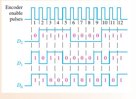
28 Comparator Applications A/D Conversion V EF Simultaneous or flash analog-to-digital converters use 2 n -1 comparators to convert an analog input to a digital value for processing. Flash ADCs are a series of comparators, each with a slightly different reference voltage. The priority encoder produces an output equal to the highest value input. V in (analog) Op-amp comparators (7) (6) (5) (4) (3) (2) (1) (0) Priority encoder D 2 D 1 D 0 Binary output In IC flash converters, the priority encoder usually includes a latch that holds the converter data constant for a period of time after the conversion. + + Enable input
29 Example
30
31 Summing Amplifier A summing amplifier has two or more inputs and its output is the negative algebraic sum of its input voltages. A two-input summing amplifier is shown. Both the input voltages are applied to the inverting input. The output voltage for the amplifier can be written as VV OOOOOO = II 1 + II 2 ff = VV IIII1 1 If all three of the resistors are equal, then: VV OOOOOO = VV IIII1 + VV IIII2 + VV IIII2 2 ff
32 Summing Amplifier The previous equation shows that the output voltage has the same magnitude as the sum of the two input voltages but with negative sign. A general expression for a unity-gain summing amplifier with n inputs as shown in Figure where all resistances are equal is given by: VV OOOOOO = VV IIII1 + VV IIII2 + VV IIII3 + + VV IIIIII
33 Summing Amplifier What is V OUT if the input voltages are +5.0 V, 3.5 V and +4.2 V and all resistors = 10 kω? 1 f V IN1 V IN2 2 3 V OUT V IN3 + V OUT = (V IN1 + V IN2 + V IN3 ) 10 kω = (+5.0 V 3.5 V V) = 5.7 V
34 Summing Amplifier Determine the output voltage for the summing amplifier = 5.7 V
35 Averaging Amplifier An averaging amplifier is basically a summing amplifier with the gain set to f / = 1/n (n is the number of inputs). The output is the negative average of the inputs. What is V OUT if the input voltages are +5.0 V, 3.5 V and +4.2 V? Assume 1 = 2 = 3 = 10 kω and f = 3.3 kω? V OUT = ⅓(V IN1 + V IN2 + V IN3 ) = ⅓(+5.0 V 3.5 V V) V IN1 V IN f 3.3 kω V OUT = 1.9 V V IN3 +
36 Scaling Adder A scaling adder has two or more inputs with each input having a different gain. The output represents the negative scaled sum of the inputs. Assume you need to sum the inputs from three microphones. The first two microphones require a gain of 2, but the third microphone requires a gain of 3. What are the values of the input s if f = 10 kω? f 10 kω = = = = A v1 f 10 kω = = = 3.3 kω A 3 v3 5.0 kω V IN1 V IN2 V IN f 10 kω V OUT
37 D/A Conversion An application of a scaling adder is the D/A converter circuit shown here. The resistors are inversely proportional to the binary column weights. Because of the precision required of resistors, the method is useful only for small DACs. +V f V OUT 2 3
 = 0.")
38 Example VV OOOOOO(DD0) = = 0.25 VV VV OOOOOO(DD1) = 0.5 VV, VV OOOOOO DD2 = 1 VV, VV OOOOOO(DD3) = 2 VV
39
40 /2 Ladder DAC A more widely used method for D/A conversion is the /2 ladder. The gain for D 3 is 1. Each successive input has a gain that is half of previous one. The output represents a weighted sum of all of the inputs (similar to the scaling adder). Inputs D 0 D 1 D 2 D f = V out
41 /2 Ladder DAC
42 Difference Amplifier v o = v- i = v- i v- 2 = (v v-) = Also, v + = v 2 v- 2 1 v 1 Since v - = v + v 2 o = (v v ) For 2 = v v ) 1 o = (v 1 2 This circuit is also called a differential amplifier, since it amplifies the difference between the input signals. in2 is series combination of 1 and 2 because i + is zero. For v 2 =0, in1 = 1, as the circuit reduces to an inverting amplifier. For general case, i 1 is a function of both v 1 and v 2.
43 Difference Amplifier Differential input resistance: id = 2 1 Large 1 can be used to increase id 2 becomes impractically large to maintain required gain.
44 Integrators and Differentiators Inverting configuration with general impedance 1 and 2 in inverting configuration can be replaced by Z 1 (s) and Z 2 (s). The closed-loop transfer function: V o (s) /V i (s) = -Z 2 (s) /Z 1 (s) The transmission magnitude and phase for a sinusoid input can be evaluated by replacing s with jω.
45 The Ideal Integrator C The ideal integrator is an inverting amplifier that has a capacitor in the feedback path. The output voltage is proportional to the negative integral of the input voltage. From the Figure we have V in + Ideal Integrator V out II iiii = VV iiii = II CC = CC dddd CC ii dddd VV oooooo = 1 tt ii CC VV iiii ττ dddd 0 When a constant positive input voltage in the form of a step or pulse is applied, the output is a ramp that decreases negatively until the op-amp saturates at its maximum negative level.
46 The Ideal Integrator The Output Voltage is the same as the voltage on the negative side of the capacitor. The rate at which the capacitor charges, and therefore the slope of the output ramp is:
47 The Ideal Integrator Frequency domain analysis VV oo = 1 VV ii jjωω ii CC The capacitor behaves as an open-circuit at dc (ω = 0). This means that open-loop configuration at dc (infinite gain). Any tiny dc in the input could result in output saturation
48 Practical Integrator The ideal integrator uses a capacitor in the feedback which is open to DC. This implies that for DC voltage the capacitor becomes open and the op-amp becomes open-loop. Op-amp integrating circuits must have extremely low dc offset and bias currents, because small errors are equivalent to a dc input. The ideal integrator tends to accumulate these errors, which moves the output toward saturation. Practical Integrator The practical integrator overcomes these errors the simplest method is to add a relatively large feedback resistor.
49 Practical Integrator In order to prevent integrator saturation due to infinite dc gain, parallel feedback resistance is included VV oo VV ii = 1 ii / ff + jjωω ii CC Closed-loop gain = 1/(jjωω ii CC + ii / ff ) Closed-loop gain at dc = ii / ff Closed-loop gain at high frequency = 1/jjωω ii CC The integrator characteristics is no longer ideal Large resistance f should be used for the feedback
50 Example Sketch the output wave for the shown input C V in +2.0 V 0 V V t (ms) V in 10 kω µF V out V t out Vin 2 V = = = C i ( 10 kω)( 0.1 μf) 2 V/ms +1.0 V V out 0 V V t (ms)

51 Example Find the output produced by an integrator in response to an input pulse of 1-V height and 1-ms width. Let = 10 kω and C = 10 nf. If the integrator capacitor is shunted by a 1-MΩ resistor, how will the response be modified? The op amp is specified to saturate at ±13 V. VV iiii CC = 1 10kΩ 10nF = 10 V/ms

52 Example With resistor connected across C, the 1-V pulse will provide a constant current I = 0.1 ma. This current is supplied to an STC network composed of F in parallel with C. The output will be an exponential heading toward 100 V with a time constant of f C = 10 ms For t > 1 ms, the capacitor discharges through F tword 0 Vwith time-constant of 10 ms. Op Amp saturation has no effect on the operation of this circuit
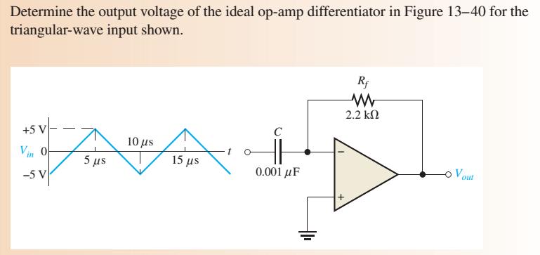
53 The Ideal Differentiator The capacitor is the input element, and the resistor is the feedback element. A differentiator produces an output that is proportional to the rate of change of the input voltage. From the Figure we have V in C + V out Ideal Differentiator II iiii = CC dddd iiii dddd = II = VV oooooo ff VV oooooo = ff CC dddd iiii dddd Apply a positive ramp voltage to the input, the output is constant equals ff CC multiplied by the slope of the ramp.
54 The Ideal Differentiator When input is a positive-going ramp, the output is negative (capacitor is charging) When input is a negative-going ramp, the output is positive (capacitor is discharging) current in the opposite direction
55
56 Practical Differentiator f V in in C V out c + The small reactance of C at high frequencies means an ideal differentiator circuit has very high gain for high-frequency noise. To compensate for this, a small series resistor is often added to the input. This practical differentiator has reduced high frequency gain and is less prone to noise.
57 Selected Key Terms Hysteresis Characteristics of a circuit in which two different trigger levels produce an offset or lag in the switching action. Schmitt A comparator with built-in hysteresis. trigger The process of limiting the output range of an Bounding amplifier or other circuit. A circuit that produces an output that approximates Integrator the area under the curve of the input function. A circuit that produces an output that approximates Differentiator the instantaneous rate of change of the input function.
58 Quiz 1. The signal that you would expect at the output of the comparator (red arrow) is a a. series of alternating positive and negative triggers b. sine wave c. square wave d. dc level V in Comparator + Differentiator C etriggerable one-shot
59 Quiz 2. Hysteresis is incorporated in a comparator by adding a. a capacitor in series with the input b. capacitors from the power supply to ground c. a small resistor in series with the input d. positive feedback
60 Quiz 3. To find the trigger points for a Schmitt trigger, you can a. divide the saturation voltage by two b. apply Kirchhoff s Voltage Law c. apply the voltage-divider rule d. calculate the rate of change of the input
61 Quiz 4. A comparator output can be limited (bounded) by a. reversing the power supply voltages b. putting a zener diode in a feedback path c. decreasing the input resistance d. connecting the inverting input to ground
62 Quiz 5. Assume all resistors in the circuit shown here have the same value. The circuit is a a. summing amplifier 1 f b. averaging amplifier c. scaling adder d. none of the above V IN1 V IN2 V IN V OUT
63 Quiz 6. Assume all resistors in the circuit shown here have different values. The circuit is a a. summing amplifier 1 f b. averaging amplifier c. scaling adder d. none of the above V IN1 V IN2 V IN V OUT
64 Quiz 7. The circuit shown is a a. A/D converter Inputs D 0 D 1 D 2 D 3 b. /2 ladder c. both of the above f = 2 + V out d. none of the above
65 Quiz 8. A practical integrator has a feedback resistor in parallel with C. The purpose of this resistor is to a. avoid noise b. increase the gain C f c. both of the above V in d. none of the above + Practical Integrator V out
66 Quiz 9. A certain circuit has the input and output signals shown. The circuit is a. a differentiator b. an integrator c. a scaling amplifier d. none of the above V in +1.0 V 0 V V t (ms) V out +2.0 V 0 V V t (ms)
67 Quiz 10. A differentiator circuit produces an output that is proportional to the negative of the a. sum of the inputs b. rate of change of the input c. area under the curve of the input d. none of the above
68 Quiz Answers: 1. c 6. c 2. d 7. b 3. c 8. d 4. b 9. a 5. a 10. b
IFB270 Advanced Electronic Circuits
 IFB270 Advanced Electronic Circuits Chapter 13: Basic op-amp circuits Prof. Manar Mohaisen Department of EEC Engineering Introduction Review of the Precedent Lecture Op-amp operation modes and parameters
Lecture #3 Basic Op-Amp Circuits
 Spring 2015 Benha University Faculty of Engineering at Shoubra ECE-322 Electronic Circuits (B) Lecture #3 Basic Op-Amp Circuits Instructor: Dr. Ahmad El-Banna Agenda Comparators Summing Amplifiers Integrators
Operational Amplifier (Op-Amp)
") Operational Amplifier (Op-Amp) 1 Contents Op-Amp Characteristics Op-Amp Circuits - Noninverting Amplifier - Inverting Amplifier - Comparator - Differential - Summing - Integrator - Differentiator 2 Introduction
Operational Amplifier (Op-Amp) 1 Contents Op-Amp Characteristics Op-Amp Circuits - Noninverting Amplifier - Inverting Amplifier - Comparator - Differential - Summing - Integrator - Differentiator 2 Introduction
Gechstudentszone.wordpress.com
 8.1 Operational Amplifier (Op-Amp) UNIT 8: Operational Amplifier An operational amplifier ("op-amp") is a DC-coupled high-gain electronic voltage amplifier with a differential input and, usually, a single-ended
Special-Purpose Operational Amplifier Circuits
 Special-Purpose Operational Amplifier Circuits Instrumentation Amplifier An instrumentation amplifier (IA) is a differential voltagegain device that amplifies the difference between the voltages existing
Lesson number one. Operational Amplifier Basics
 What About Lesson number one Operational Amplifier Basics As well as resistors and capacitors, Operational Amplifiers, or Op-amps as they are more commonly called, are one of the basic building blocks
Unit WorkBook 1 Level 4 ENG U22 Electronic Circuits and Devices 2018 UniCourse Ltd. All Rights Reserved. Sample
 Pearson BTEC Level 4 Higher Nationals in Engineering (RQF) Unit 22: Electronic Circuits and Devices Unit Workbook 1 in a series of 4 for this unit Learning Outcome 1 Operational Amplifiers Page 1 of 23
B.E. SEMESTER III (ELECTRICAL) SUBJECT CODE: X30902 Subject Name: Analog & Digital Electronics
 SUBJECT CODE: X30902 Subject Name: Analog & Digital Electronics") B.E. SEMESTER III (ELECTRICAL) SUBJECT CODE: X30902 Subject Name: Analog & Digital Electronics Sr. No. Date TITLE To From Marks Sign 1 To verify the application of op-amp as an Inverting Amplifier 2 To
B.E. SEMESTER III (ELECTRICAL) SUBJECT CODE: X30902 Subject Name: Analog & Digital Electronics Sr. No. Date TITLE To From Marks Sign 1 To verify the application of op-amp as an Inverting Amplifier 2 To
Lecture #4 Basic Op-Amp Circuits
 Summer 2015 Ahmad El-Banna Faculty of Engineering Department of Electronics and Communications GEE336 Electronic Circuits II Lecture #4 Basic Op-Amp Circuits Instructor: Dr. Ahmad El-Banna Agenda Some
Electronic PRINCIPLES
 MALVINO & BATES Electronic PRINCIPLES SEVENTH EDITION Chapter 22 Nonlinear Op-Amp Circuits Topics Covered in Chapter 22 Comparators with zero reference Comparators with non-zero references Comparators
Analog Electronic Circuits Code: EE-305-F
 Analog Electronic Circuits Code: EE-305-F 1 INTRODUCTION Usually Called Op Amps Section -C Operational Amplifier An amplifier is a device that accepts a varying input signal and produces a similar output
PHYS 536 The Golden Rules of Op Amps. Characteristics of an Ideal Op Amp
 PHYS 536 The Golden Rules of Op Amps Introduction The purpose of this experiment is to illustrate the golden rules of negative feedback for a variety of circuits. These concepts permit you to create and
Operational Amplifier as A Black Box
 Chapter 8 Operational Amplifier as A Black Box 8. General Considerations 8.2 Op-Amp-Based Circuits 8.3 Nonlinear Functions 8.4 Op-Amp Nonidealities 8.5 Design Examples Chapter Outline CH8 Operational Amplifier
LINEAR IC APPLICATIONS
 1 B.Tech III Year I Semester (R09) Regular & Supplementary Examinations December/January 2013/14 1 (a) Why is R e in an emitter-coupled differential amplifier replaced by a constant current source? (b)
Operational Amplifiers
 Fundamentals of op-amp Operation modes Golden rules of op-amp Op-amp circuits Inverting & non-inverting amplifier Unity follower, integrator & differentiator Introduction An operational amplifier, or op-amp,
L02 Operational Amplifiers Applications 1
 L02 Operational Amplifiers Applications 1 Chapter 9 Ideal Operational Amplifiers and Op-Amp Circuits Donald A. Neamen (2009). Microelectronics: Circuit Analysis and Design, 4th Edition, Mc-Graw-Hill Prepared
Summer 2015 Examination
 Summer 2015 Examination Subject Code: 17445 Model Answer Important Instructions to examiners: 1) The answers should be examined by key words and not as word-to-word as given in the model answer scheme.
Signal Conditioning Systems
 Note-13 1 Signal Conditioning Systems 2 Generalized Measurement System: The output signal from a sensor has generally to be processed or conditioned to make it suitable for the next stage Signal conditioning
ELT 215 Operational Amplifiers (LECTURE) Chapter 5
 Chapter 5") CHAPTER 5 Nonlinear Signal Processing Circuits INTRODUCTION ELT 215 Operational Amplifiers (LECTURE) In this chapter, we shall present several nonlinear circuits using op-amps, which include those situations
CHAPTER 5 Nonlinear Signal Processing Circuits INTRODUCTION ELT 215 Operational Amplifiers (LECTURE) In this chapter, we shall present several nonlinear circuits using op-amps, which include those situations
EXPERIMENT 2.2 NON-LINEAR OP-AMP CIRCUITS
 2.16 EXPERIMENT 2.2 NONLINEAR OPAMP CIRCUITS 2.2.1 OBJECTIVE a. To study the operation of 741 opamp as comparator. b. To study the operation of active diode circuits (precisions circuits) using opamps,
LESSON PLAN. SUBJECT: LINEAR IC S AND APPLICATION NO OF HOURS: 52 FACULTY NAME: Mr. Lokesh.L, Hema. B DEPT: ECE. Portions to be covered
 LESSON PLAN SUBJECT: LINEAR IC S AND APPLICATION SUB CODE: 15EC46 NO OF HOURS: 52 FACULTY NAME: Mr. Lokesh.L, Hema. B DEPT: ECE Class# Chapter title/reference literature Portions to be covered MODULE I
Oscillators. An oscillator may be described as a source of alternating voltage. It is different than amplifier.
 Oscillators An oscillator may be described as a source of alternating voltage. It is different than amplifier. An amplifier delivers an output signal whose waveform corresponds to the input signal but
Section 4: Operational Amplifiers
 Section 4: Operational Amplifiers Op Amps Integrated circuits Simpler to understand than transistors Get back to linear systems, but now with gain Come in various forms Comparators Full Op Amps Differential
About the Tutorial. Audience. Prerequisites. Copyright & Disclaimer. Linear Integrated Circuits Applications
 About the Tutorial Linear Integrated Circuits are solid state analog devices that can operate over a continuous range of input signals. Theoretically, they are characterized by an infinite number of operating
Chapter 2. Operational Amplifiers
 Chapter 2. Operational Amplifiers Tong In Oh 1 2.5 Integrators and Differentiators Utilized resistors in the op-amp feedback and feed-in path Ideally independent of frequency Use of capacitors together
Difference between BJTs and FETs. Junction Field Effect Transistors (JFET)
") Difference between BJTs and FETs Transistors can be categorized according to their structure, and two of the more commonly known transistor structures, are the BJT and FET. The comparison between BJTs
Difference between BJTs and FETs Transistors can be categorized according to their structure, and two of the more commonly known transistor structures, are the BJT and FET. The comparison between BJTs
CMOS Schmitt Trigger A Uniquely Versatile Design Component
 CMOS Schmitt Trigger A Uniquely Versatile Design Component INTRODUCTION The Schmitt trigger has found many applications in numerous circuits, both analog and digital. The versatility of a TTL Schmitt is
Chapter 13 Oscillators and Data Converters
 Chapter 13 Oscillators and Data Converters 13.1 General Considerations 13.2 Ring Oscillators 13.3 LC Oscillators 13.4 Phase Shift Oscillator 13.5 Wien-Bridge Oscillator 13.6 Crystal Oscillators 13.7 Chapter
ES250: Electrical Science. HW6: The Operational Amplifier
 ES250: Electrical Science HW6: The Operational Amplifier Introduction This chapter introduces the operational amplifier or op amp We will learn how to analyze and design circuits that contain op amps,
Operational amplifiers
 Operational amplifiers Bởi: Sy Hien Dinh INTRODUCTION Having learned the basic laws and theorems for circuit analysis, we are now ready to study an active circuit element of paramount importance: the operational
Sine-wave oscillator
 Sine-wave oscillator In Fig. 1, an op-'amp can be made to oscillate by feeding a portion of the output back to the input via a frequency-selective network, and controlling the overall voltage gain. For
C H A P T E R 02. Operational Amplifiers
 C H A P T E R 02 Operational Amplifiers The Op-amp Figure 2.1 Circuit symbol for the op amp. Figure 2.2 The op amp shown connected to dc power supplies. The Ideal Op-amp 1. Infinite input impedance 2.
IFB270 Advanced Electronic Circuits
 IFB270 Advanced Electronic Circuits Chapter 14: Special-purpose op-amp circuits Prof. Manar Mohaisen Department of EEC Engineering eview of the Precedent Lecture Introduce the level detection op-amp circuits
LM13600 Dual Operational Transconductance Amplifiers with Linearizing Diodes and Buffers
 LM13600 Dual Operational Transconductance Amplifiers with Linearizing Diodes and Buffers General Description The LM13600 series consists of two current controlled transconductance amplifiers each with
Data Converters. Dr.Trushit Upadhyaya EC Department, CSPIT, CHARUSAT
 Data Converters Dr.Trushit Upadhyaya EC Department, CSPIT, CHARUSAT Purpose To convert digital values to analog voltages V OUT Digital Value Reference Voltage Digital Value DAC Analog Voltage Analog Quantity:
OPERATIONAL AMPLIFIER PREPARED BY, PROF. CHIRAG H. RAVAL ASSISTANT PROFESSOR NIRMA UNIVRSITY
 OPERATIONAL AMPLIFIER PREPARED BY, PROF. CHIRAG H. RAVAL ASSISTANT PROFESSOR NIRMA UNIVRSITY INTRODUCTION Op-Amp means Operational Amplifier. Operational stands for mathematical operation like addition,
Infrared Communications Lab
 Infrared Communications Lab This lab assignment assumes that the student knows about: Ohm s Law oltage, Current and Resistance Operational Amplifiers (See Appendix I) The first part of the lab is to develop
BME/ISE 3512 Bioelectronics. Laboratory Five - Operational Amplifiers
 BME/ISE 3512 Bioelectronics Laboratory Five - Operational Amplifiers Learning Objectives: Be familiar with the operation of a basic op-amp circuit. Be familiar with the characteristics of both ideal and
GATE SOLVED PAPER - IN
 YEAR 202 ONE MARK Q. The i-v characteristics of the diode in the circuit given below are : v -. A v 0.7 V i 500 07 $ = * 0 A, v < 0.7 V The current in the circuit is (A) 0 ma (C) 6.67 ma (B) 9.3 ma (D)
DIGITAL ELECTRONICS WAVE SHAPING AND PULSE CIRCUITS. September 2012
 AM 5-403 DIGITAL ELECTRONICS WAVE SHAPING AND PULSE CIRCUITS September 2012 DISTRIBUTION RESTRICTION: Approved for public release. Distribution is unlimited. DEPARTMENT OF THE ARMY MILITARY AUXILIARY RADIO
INTEGRATED CIRCUITS. AN109 Microprocessor-compatible DACs Dec
 INTEGRATED CIRCUITS 1988 Dec DAC products are designed to convert a digital code to an analog signal. Since a common source of digital signals is the data bus of a microprocessor, DAC circuits that are
Figure 1.1 Mechatronic system components (p. 3)
") Figure 1.1 Mechatronic system components (p. 3) Example 1.2 Measurement System Digital Thermometer (p. 5) Figure 2.2 Electric circuit terminology (p. 13) Table 2.2 Resistor color band codes (p. 18) Figure
Figure 1.1 Mechatronic system components (p. 3) Example 1.2 Measurement System Digital Thermometer (p. 5) Figure 2.2 Electric circuit terminology (p. 13) Table 2.2 Resistor color band codes (p. 18) Figure
Differential Amplifier : input. resistance. Differential amplifiers are widely used in engineering instrumentation
 Differential Amplifier : input resistance Differential amplifiers are widely used in engineering instrumentation Differential Amplifier : input resistance v 2 v 1 ir 1 ir 1 2iR 1 R in v 2 i v 1 2R 1 Differential
Interface Electronic Circuits
 Lecture (5) Interface Electronic Circuits Part: 1 Prof. Kasim M. Al-Aubidy Philadelphia University-Jordan AMSS-MSc Prof. Kasim Al-Aubidy 1 Interface Circuits: An interface circuit is a signal conditioning
DEPARTMENT OF ELECTRICAL ENGINEERING AND COMPUTER SCIENCE MASSACHUSETTS INSTITUTE OF TECHNOLOGY CAMBRIDGE, MASSACHUSETTS 02139
 DEPARTMENT OF ELECTRICAL ENGINEERING AND COMPUTER SCIENCE MASSACHUSETTS INSTITUTE OF TECHNOLOGY CAMBRIDGE, MASSACHUSETTS 019.101 Introductory Analog Electronics Laboratory Laboratory No. READING ASSIGNMENT
11. Chapter: Amplitude stabilization of the harmonic oscillator
 Punčochář, Mohylová: TELO, Chapter 10 1 11. Chapter: Amplitude stabilization of the harmonic oscillator Time of study: 3 hours Goals: the student should be able to define basic principles of oscillator
BME 3512 Bioelectronics Laboratory Five - Operational Amplifiers
 BME 351 Bioelectronics Laboratory Five - Operational Amplifiers Learning Objectives: Be familiar with the operation of a basic op-amp circuit. Be familiar with the characteristics of both ideal and real
Analytical Chemistry II
 Analytical Chemistry II L3: Signal processing (selected slides) Semiconductor devices Apart from resistors and capacitors, electronic circuits often contain nonlinear devices: transistors and diodes. The
Applied Electronics II
 Applied Electronics II Chapter 3: Operational Amplifier Part 1- Op Amp Basics School of Electrical and Computer Engineering Addis Ababa Institute of Technology Addis Ababa University Daniel D./Getachew
UNIT I. Operational Amplifiers
 UNIT I Operational Amplifiers Operational Amplifier: The operational amplifier is a direct-coupled high gain amplifier. It is a versatile multi-terminal device that can be used to amplify dc as well as
Operational Amplifiers
 Operational Amplifiers for Basic Electronics http://cktse.eie.polyu.edu.hk/eie209 by Prof. Michael Tse January 2005 Where do we begin? We begin with assuming that the op-amp is an ideal element satisfying
Operational Amplifiers (Op Amps)
") Operational Amplifiers (Op Amps) Introduction * An operational amplifier is modeled as a voltage controlled voltage source. * An operational amplifier has a very high input impedance and a very high gain.
Operational Amplifiers (Op Amps) Introduction * An operational amplifier is modeled as a voltage controlled voltage source. * An operational amplifier has a very high input impedance and a very high gain.
Chapter 14 Operational Amplifiers
 1. List the characteristics of ideal op amps. 2. Identify negative feedback in op-amp circuits. 3. Analyze ideal op-amp circuits that have negative feedback using the summing-point constraint. ELECTRICAL
Chapter 2. Operational Amplifiers
 Chapter 2. Operational Amplifiers Tong In Oh 1 Objective Terminal characteristics of the ideal op amp How to analyze op amp circuits How to use op amps to design amplifiers How to design more sophisticated
1) Consider the circuit shown in figure below. Compute the output waveform for an input of 5kHz
 Consider the circuit shown in figure below. Compute the output waveform for an input of 5kHz") ) Consider the circuit shown in figure below. Compute the output waveform for an input of 5kHz Solution: a) Input is of constant amplitude of 2 V from 0 to 0. ms and 2 V from 0. ms to 0.2 ms. The output
) Consider the circuit shown in figure below. Compute the output waveform for an input of 5kHz Solution: a) Input is of constant amplitude of 2 V from 0 to 0. ms and 2 V from 0. ms to 0.2 ms. The output
State the application of negative feedback and positive feedback (one in each case)
") (ISO/IEC - 700-005 Certified) Subject Code: 073 Model wer Page No: / N Important Instructions to examiners: ) The answers should be examined by key words and not as word-to-word as given in the model answer
(ISO/IEC - 700-005 Certified) Subject Code: 073 Model wer Page No: / N Important Instructions to examiners: ) The answers should be examined by key words and not as word-to-word as given in the model answer
Q1. Explain the Astable Operation of multivibrator using 555 Timer IC.
 Q1. Explain the Astable Operation of multivibrator using 555 Timer I. Answer: The following figure shows the 555 Timer connected for astable operation. A V PIN 8 PIN 7 B 5K PIN6 - S Q 5K PIN2 - Q PIN3
Homework Assignment 07
 Homework Assignment 07 Question 1 (Short Takes). 2 points each unless otherwise noted. 1. A single-pole op-amp has an open-loop low-frequency gain of A = 10 5 and an open loop, 3-dB frequency of 4 Hz.
Homework Assignment 03
 Homework Assignment 03 Question 1 (Short Takes), 2 points each unless otherwise noted. 1. Two 0.68 μf capacitors are connected in series across a 10 khz sine wave signal source. The total capacitive reactance
+ power. V out. - power +12 V -12 V +12 V -12 V
 Question 1 Questions An operational amplifier is a particular type of differential amplifier. Most op-amps receive two input voltage signals and output one voltage signal: power 1 2 - power Here is a single
Analog Circuits Part 3 Operational Amplifiers
 Introductory Medical Device Prototyping Analog Circuits Part 3 Operational Amplifiers, http://saliterman.umn.edu/ Department of Biomedical Engineering, University of Minnesota Concepts to be Reviewed Operational
inverting V CC v O -V EE non-inverting
 Chapter 4 Operational Amplifiers 4.1 Introduction The operational amplifier (opamp for short) is perhaps the most important building block for the design of analog circuits. Combined with simple negative
Analog I/O. ECE 153B Sensor & Peripheral Interface Design Winter 2016
 Analog I/O ECE 153B Sensor & Peripheral Interface Design Introduction Anytime we need to monitor or control analog signals with a digital system, we require analogto-digital (ADC) and digital-to-analog
Operational Amplifiers
 CHAPTER 5 Operational Amplifiers Operational amplifiers (or Op Amp) is an active circuit element that can perform mathematical operations between signals (e.g., amplify, sum, subtract, multiply, divide,
Linear IC s and applications
 Questions and Solutions PART-A Unit-1 INTRODUCTION TO OP-AMPS 1. Explain data acquisition system Jan13 DATA ACQUISITION SYSYTEM BLOCK DIAGRAM: Input stage Intermediate stage Level shifting stage Output
INTEGRATED CIRCUITS AND APPLICATIONS LAB MANUAL
 INTEGRATED CIRCUITS AND APPLICATIONS LAB MANUAL V SEMESTER Department of Electronics and communication Engineering Government Engineering College, Dahod-389151 http://www.gecdahod.ac.in/ L A B M A N U
ELEC207 LINEAR INTEGRATED CIRCUITS
 Concept of VIRTUAL SHORT For feedback amplifiers constructed with op-amps, the two op-amp terminals will always be approximately equal (V + = V - ) This condition in op-amp feedback amplifiers is known
An active filter offers the following advantages over a passive filter:
 ACTIVE FILTERS An electric filter is often a frequency-selective circuit that passes a specified band of frequencies and blocks or attenuates signals of frequencies outside this band. Filters may be classified
Operational Amplifiers
 Operational Amplifiers Table of contents 1. Design 1.1. The Differential Amplifier 1.2. Level Shifter 1.3. Power Amplifier 2. Characteristics 3. The Opamp without NFB 4. Linear Amplifiers 4.1. The Non-Inverting
Precision Rectifier Circuits
 Precision Rectifier Circuits Rectifier circuits are used in the design of power supply circuits. In such applications, the voltage being rectified are usually much greater than the diode voltage drop,
In-Class Exercises for Lab 2: Input and Output Impedance
 In-Class Exercises for Lab 2: Input and Output Impedance. What is the output resistance of the output device below? Suppose that you want to select an input device with which to measure the voltage produced
Homework Assignment 07
 Homework Assignment 07 Question 1 (Short Takes). 2 points each unless otherwise noted. 1. A single-pole op-amp has an open-loop low-frequency gain of A = 10 5 and an open loop, 3-dB frequency of 4 Hz.
PAiA 4780 Twelve Stage Analog Sequencer Design Analysis Originally published 1974
 PAiA 4780 Twelve Stage Analog Sequencer Design Analysis Originally published 1974 DESIGN ANALYSIS: CLOCK As is shown in the block diagram of the sequencer (fig. 1) and the schematic (fig. 2), the clock
LM125 Precision Dual Tracking Regulator
 LM125 Precision Dual Tracking Regulator INTRODUCTION The LM125 is a precision, dual, tracking, monolithic voltage regulator. It provides separate positive and negative regulated outputs, thus simplifying
CENG4480 Lecture 04: Analog/Digital Conversions
 CENG4480 Lecture 04: Analog/Digital Conversions Bei Yu byu@cse.cuhk.edu.hk (Latest update: October 3, 2018) Fall 2018 1 / 31 Overview Preliminaries Comparator Digital to Analog Conversion (DAC) Analog
LM13700 Dual Operational Transconductance Amplifiers with Linearizing Diodes and Buffers
 LM13700 Dual Operational Transconductance Amplifiers with Linearizing Diodes and Buffers General Description The LM13700 series consists of two current controlled transconductance amplifiers, each with
EECE251 Circuit Analysis I Set 5: Operational Amplifiers
 EECE251 Circuit Analysis I Set 5: Operational Amplifiers Shahriar Mirabbasi Department of Electrical and Computer Engineering University of British Columbia shahriar@ece.ubc.ca 1 Amplifiers There are various
ANALOG ELECTRONIC CIRCUITS (EE-325-F) LAB MANUAL
 LAB MANUAL") ANALOG ELECTRONIC CIRCUITS (EE-325-F) LAB MANUAL V SEMESTER Department Of Electronics & CommunicationEngg. BSA Institute of Technology & Management Faridabad. LIST OF EXPERIMENTS S.NO. NAME OF THE EXPERIMENT
ANALOG ELECTRONIC CIRCUITS (EE-325-F) LAB MANUAL V SEMESTER Department Of Electronics & CommunicationEngg. BSA Institute of Technology & Management Faridabad. LIST OF EXPERIMENTS S.NO. NAME OF THE EXPERIMENT
Unit 6 Operational Amplifiers Chapter 5 (Sedra and Smith)
") Unit 6 Operational Amplifiers Chapter 5 (Sedra and Smith) Prepared by: S V UMA, Associate Professor, Department of ECE, RNSIT, Bangalore Reference: Microelectronic Circuits Adel Sedra and K C Smith 1 Objectives
Unit 6 Operational Amplifiers Chapter 5 (Sedra and Smith) Prepared by: S V UMA, Associate Professor, Department of ECE, RNSIT, Bangalore Reference: Microelectronic Circuits Adel Sedra and K C Smith 1 Objectives
Homework Assignment True or false. For both the inverting and noninverting op-amp configurations, V OS results in
 Question 1 (Short Takes), 2 points each. Homework Assignment 02 1. An op-amp has input bias current I B = 1 μa. Make an estimate for the input offset current I OS. Answer. I OS is normally an order of
Integrated Circuit: Classification:
 Integrated Circuit: It is a miniature, low cost electronic circuit consisting of active and passive components that are irreparably joined together on a single crystal chip of silicon. Classification:
Transistor Design & Analysis (Inverter)
") Experiment No. 1: DIGITAL ELECTRONIC CIRCUIT Transistor Design & Analysis (Inverter) APPARATUS: Transistor Resistors Connecting Wires Bread Board Dc Power Supply THEORY: Digital electronics circuits operate
Experiment No. 1: DIGITAL ELECTRONIC CIRCUIT Transistor Design & Analysis (Inverter) APPARATUS: Transistor Resistors Connecting Wires Bread Board Dc Power Supply THEORY: Digital electronics circuits operate
Applied Electronics II
 Applied Electronics II Chapter 4: Wave shaping and Waveform Generators School of Electrical and Computer Engineering Addis Ababa Institute of Technology Addis Ababa University Daniel D./Getachew T./Abel
DEPARTMENT OF ELECTRICAL ENGINEERING AND COMPUTER SCIENCE MASSACHUSETTS INSTITUTE OF TECHNOLOGY CAMBRIDGE, MASSACHUSETTS 02139
 DEPARTMENT OF ELECTRICAL ENGINEERING AND COMPUTER SCIENCE MASSACHUSETTS INSTITUTE OF TECHNOLOGY CAMBRIDGE, MASSACHUSETTS 019 Spring Term 00.101 Introductory Analog Electronics Laboratory Laboratory No.
Experiments #7. Operational Amplifier part 1
 Experiments #7 Operational Amplifier part 1 1) Objectives: The objective of this lab is to study operational amplifier (op amp) and its applications. We will be simulating and building some basic op-amp
55:141 Advanced Circuit Techniques Switching Regulators
 55:141 Advanced Circuit Techniques Switching Regulators Material: ecture Notes, Handouts, and Sections of Chapter 11 of Franco A. Kruger 55:141: Advanced Circuit Techniques The University of Iowa Switching
EE301 ELECTRONIC CIRCUITS CHAPTER 2 : OSCILLATORS. Lecturer : Engr. Muhammad Muizz Bin Mohd Nawawi
 EE301 ELECTRONIC CIRCUITS CHAPTER 2 : OSCILLATORS Lecturer : Engr. Muhammad Muizz Bin Mohd Nawawi 2.1 INTRODUCTION An electronic circuit which is designed to generate a periodic waveform continuously at
HIGH LOW Astable multivibrators HIGH LOW 1:1
 1. Multivibrators A multivibrator circuit oscillates between a HIGH state and a LOW state producing a continuous output. Astable multivibrators generally have an even 50% duty cycle, that is that 50% of
Test Your Understanding
 074 Part 2 Analog Electronics EXEISE POBLEM Ex 5.3: For the switched-capacitor circuit in Figure 5.3b), the parameters are: = 30 pf, 2 = 5pF, and F = 2 pf. The clock frequency is 00 khz. Determine the
Chapter 9: Operational Amplifiers
 Chapter 9: Operational Amplifiers The Operational Amplifier (or op-amp) is the ideal, simple amplifier. It is an integrated circuit (IC). An IC contains many discrete components (resistors, capacitors,
Chapter 9: Operational Amplifiers
 Chapter 9: Operational Amplifiers The Operational Amplifier (or op-amp) is the ideal, simple amplifier. It is an integrated circuit (IC). An IC contains many discrete components (resistors, capacitors,
SKEU 3741 BASIC ELECTRONICS LAB
 Faculty: Subject Subject Code : SKEU 3741 FACULTY OF ELECTICAL ENGINEEING : 2 ND YEA ELECTONIC DESIGN LABOATOY eview elease Date Last Amendment Procedure Number : 1 : 2013 : 2013 : PK-UTM-FKE-(0)-10 SKEU
The steeper the phase shift as a function of frequency φ(ω) the more stable the frequency of oscillation
 the more stable the frequency of oscillation") It should be noted that the frequency of oscillation ω o is determined by the phase characteristics of the feedback loop. the loop oscillates at the frequency for which the phase is zero The steeper the
It should be noted that the frequency of oscillation ω o is determined by the phase characteristics of the feedback loop. the loop oscillates at the frequency for which the phase is zero The steeper the
LIC & COMMUNICATION LAB MANUAL
 LIC & Communication Lab Manual LIC & COMMUNICATION LAB MANUAL FOR V SEMESTER B.E (E& ( E&C) (For private circulation only) NAME: DEPARTMENT OF ELECTRONICS & COMMUNICATION SRI SIDDHARTHA INSTITUTE OF TECHNOLOGY
Microprocessor based process control
 Microprocessor based process control Presented by Dr. Walid Ghoneim Lecture on: Op Amps and Their Applications in Signal Conditioning References: Op Amps for Everyone, MANCINI, R. (2002). The Forrest Mims
Facility of Engineering. Biomedical Engineering Department. Medical Electronic Lab BME (317) Post-lab Forms
 Post-lab Forms") Facility of Engineering Biomedical Engineering Department Medical Electronic Lab BME (317) Post-lab Forms Prepared by Eng.Hala Amari Spring 2014 Facility of Engineering Biomedical Engineering Department
Facility of Engineering Biomedical Engineering Department Medical Electronic Lab BME (317) Post-lab Forms Prepared by Eng.Hala Amari Spring 2014 Facility of Engineering Biomedical Engineering Department
Comparators, positive feedback, and relaxation oscillators
 Experiment 4 Introductory Electronics Laboratory Comparators, positive feedback, and relaxation oscillators THE SCHMITT TRIGGER AND POSITIVE FEEDBACK 4-2 The op-amp as a comparator... 4-2 Using positive
CHAPTER 1 DIODE CIRCUITS. Semiconductor act differently to DC and AC currents
 CHAPTER 1 DIODE CIRCUITS Resistance levels Semiconductor act differently to DC and AC currents There are three types of resistances 1. DC or static resistance The application of DC voltage to a circuit
Diode Circuits Recent GATE Problems
 Diode Circuits Recent GATE Problems 1. The diodes and capacitors in the circuit shown are ideal. The voltage v(t) across the diode DD 1 is CC 1 DD 2 cos(ωωωω) AC DD 1 CC 1 (a) cos(ωωωω) 1 (b) sin(ωωωω)
Homework Assignment Consider the circuit shown. Assume ideal op-amp behavior. Which statement below is true?
 Question 1 (2 points each unless noted otherwise) Homework Assignment 03 1. Consider the circuit shown. Assume ideal op-amp behavior. Which statement below is true? (a) V = VV + = 5 V (op-amp operation)