CHAPTER 1 DIODE CIRCUITS. Semiconductor act differently to DC and AC currents
|
|
|
- Daisy Chandler
- 6 years ago
- Views:
Transcription
1 CHAPTER 1 DIODE CIRCUITS Resistance levels Semiconductor act differently to DC and AC currents There are three types of resistances 1. DC or static resistance The application of DC voltage to a circuit containing a semiconductor diode will result in an operating point on the characteristics curve that will not change with time. i.e. For specified applied voltage the diode will have a specified current I d and specified resistance R D. The resistance of the diode depends on applied voltage V D and can be found by The D.C resistance levels at the knee and below will be greater than the resistance levels obtained for the vertical section of the charecterstics. The resistance levels in the reverse bias region will naturally quite high. Also higher the current through the diode the lower is the resistance level. 2. AC or dynamic resistance The varying input will move the instantaneous operating point up and down a region of characteristics. 1
2 Without AC signal applied to the diode the operating point Q which is fixed not moving hence it is called Quiescent point or Q point. A straight line drawn tangent to the curve through the Q point as shown in the figure will define particular change in voltage and current that can be used to determine AC or dynamic resistance for this region of diode characteristics. The steeper the slope, the lower is the value of for the same change in, and there by lowering the value of resistance. The A.C resistance in the vertical-rise region of the characteristics is quite small, Whereas A.C resistance is much higher at low current levels. The lower the Q point of operation, the higher is the A.C resistance. Mathematical expression of AC resistance We have [ ] [ ] 2
3 Where Hence Flipping the result we have Note: Substituting n =1 and V T = 26mV We have Observation The equation can be used directly by substituting Q point diode current I D to find the AC resistance. At lower values of I D, and the value of obtained must be multiplied by factor of 2. For small values of below the knee of the curve, the equation becomes inappropriate. Every diode has some resistance due to resistance of semiconductor material which is called body resistance and the resistance introduced by the connection between the semiconductor material and external metallic conductor called contact resistance. These can be included in the equation i.e. 3
4 Average AC resistance If the input signal is sufficiently large to produce a broad swing as indicated in figure the resistance associated with the device for this region is called average AC resistance. The average AC resistance is determined by a straight line drawn between the two intersections established by the maximum and minimum values of the input signal voltages. 4
5 Summary Type Equation Special characteristics Graphical determinations DC or static resistance Defined as a point on the characteristics AC or Dynamic resistance Defined by a tangent line at the Q point Average AC Defined by a straight line between limits of operation Diode Equivalent Circuits An equivalent circuit is combination of elements properly chosen to best represent the characteristics of a device in a particular operating region. Piecewise linear equivalent circuit The equivalent circuit for a diode can be obtained by approximating the characteristics of the diode by straight line segment which is as shown in the figure 5

6 The barrier potential which is equal in magnitude to the cut in voltage is represented as a battery of e.m.f V K The resistance r av offered by the forward bias diode is shown as an external resistance in series with the ideal diode. Simplified equivalent circuit For most application the resistance r av is quite small compared to the other elements in the network. So removing r av from the equivalent circuit the characteristics of the diode is as shown in the figure, along with reduced equivalent circuit. 6
7 Ideal equivalent circuit Let us ignore both resistance and cutoff voltage V K = 0.7V. In the case the equivalent circuit will be reduced to that of an ideal diode as shown in figure Transition and diffusion capacitance Every electronic or electrical device is frequency sensitive. In the p-n semiconductor diode, there are two capacitive effects to be considered 1. Transition capacitance 2. Diffusion capacitance The basic equation for the capacitance of a parallel plate capacitor is defined as Where Transition capacitance In the reverse bias region there is a depletion region that behaves essentially like an insulator between the layers of opposite charge. As the voltage is increased the depletion region widens and hence its capacitances decreases. 7
8 Diffusion capacitance In forward bias region the width of the depletion region is much reduced resulting in the increased levels of current that will result in increased level of diffusion current. Reverse Recovery time The diode conducts rapidly when forward biased and blocks conduction when reverse biased. If the applied voltage is reversed to establish a reverse bias situation we would ideally like to see the diode change instantaneously from the conduction state to non conduction state, however the diode current will simply reverse as shown in figure and stay at this level for the period of time t s (storage time) required for minority carrier to move into other region, after this reverse current decreases exponentially for a time t t (transition time). 8
9 Load line analysis Let us consider a diode D in series with a load resistance R. The diode characteristics are placed on the same set of axis as a straight line defined by the parameters of network. The intersection on the vertical axis is defined by applied load R. Hence the analysis is therefore called load line analysis Applying KVL to the circuit Hence When V D = 0, we have When I D = 0, we have E A straight line drawn between the two points will define load line which is as shown in the figure Change the value of R and the intersection on the vertical axis will change. The result will be a different point of intersection between the load line and device characteristics. 9
10 The point of operation is called Quiescent point which gives current through diode for given load and input voltage By mathematically calculate we have from equation (1) And Example 1. For the series diode configuration of fig (a) employing the diode characteristics of figure (b) Determine I) II) Fig. a Fig.b I. 10
11 From the resulting load line analysis we find II. 2. Repeat the above problem for Approximate equivalent model we have The level of remains same 11
12 3. Repeat the above problem for for ideal diode model We have Rectification Rectification is the process of converting alternating current into direct current. Rectifier Rectifier is device that converts AC current into DC current (pulsating DC) Half wave rectifier The following figure shows the half wave rectifier circuit. An alternating input voltage is applied to the diode connected in series with load resistance R During the interval t = 0 T/2 The polarity of V i makes the diode to turn ON this provides short circuit equivalence for the ideal diode. The output signal is exact replica of the applied signal which is as shown in figure 12
13 During the interval t = T/2 T The polarity of V i makes the diode to turn off. This provides open circuit equivalence for the ideal diode. The result is absence of path which is as shown in the figure When we sketch input V i and the outputs together then we get The D.C output waveform is expected tobe a straight line but the half wave rectifier gives output in The D.C output waveform is expected to be a straight line but the halfwave rectifier gives output in the form of positive sinusoidal pulses. The average value of D.C voltage is given by 13
14 Since we are using silicon diode we have a cut-in voltage V K of 0.7V. Hence the diode will be in off state when V i is less than 0.7V hence output will be zero which is as shown in figure. The net effect is reduction in area which reduces the average DC voltage hence Note: One complete cycle 0 to 2Π. To find he average value of alternating waveform, we have to determine the area under the curve one complete cycle and then dividing it by the base i.e 2 Π I m peak value of load current 2Π Π current flows only in positive half cycle [ ] [ ] 14
15 Average D.C load voltage Neglecting the internal resistance we have Example 1. Sketch the output V o and determine the DC level of the output for the network of figure (a) 2. Repeat part (a) if the ideal diode is replaced by a silicon diode 3. Repeat part (a) and (b) if V m is increased to 200V and compare solutions. Using equation (1) and (2). Solution 1. The diode will conduct for negative half cycle hence the output is as shonwn in figure 15
16 2. For silicon diode. 3. Peak inverse voltage (PIV) or Peak reverse voltage (PRV) The peak inverse voltage rating of the diode is of primary importance in the design of rectification system. It is the voltage rating that must not be exceeded in the reverse bias region. The required PIV rating can be determined from the following figure. Full wave reactivation The following figure shows the full-wave bridge rectifier circuit with four diodes in a bridge configuration. An alternating in out is applied to diodes with a load resistance R. 16
17 During the interval t = 0 T/2 The polarity of input V i makes the diodes D 2 and D 3 to turn ON whereas D 1 and D 3 to turn off which is as shown in figure. Since the diodes are ideal, the load voltage is V o = V i. During the interval t = T/2 T The polarity of input V i makes the diodes D 1 and D 4 to turn ON where as D 2 and D 3 to turn off which is as shown in figure. Since the diodes are ideal the polarity across the load resistor R is same as shown in figure (a) thus establishing a second positive pulse as shown in figure (b) When we sketch input V i and the outputs together we get 17
18 The D.C output waveform is expected to be a straight line but the full wave rectifier gives output in the form of positive sinusoidal pulses. The average value of D.C voltage is given by If we use silicon diode as shown in the figure the application of KVL around the conduction path result in The peak output voltage is therefore The DC voltage of silicon diode Peak inverse voltage (PIV) or Peak reverse voltage (PRV) The required PIV rating can be determined from the following figure 18
19 Center tapped transformer The following figure shows the full wave rectifier circuit with only two diodes, but requiring a center tapped transformer to establish the input signal across each section of the secondary of the transformer. During the interval t = 0 T/2 The positive portion of V i applied to primary of the transformer. The polarity of V i makes the diode D 1 to turn ON where as D 2 to turn off which is as shown in figure During the interval t = T/2 T The negative portion of V i applied to primary of the transformer. The polarity of V i makes the diode D 2 to turn ON where as D 1 to turn off which is as shown in the figure 19
20 When we sketch input Vi and the outputs together we get Peak inverse voltage (PIV) or Peak reverse voltage (PRV) The required PIV rating can be determined from the following figure Example Determine the output waveform for the network of figure and calculate the output DC level and the required PIV of each diode. Solution The network appears as shown in the figure below for the positive region of the input voltage 20
21 Redrawing the above circuit we have Applying voltage divider rule we have Hence For the negative part of the input the roles of the diodes are interchanged and V o appears as shown below 21
22 Clippers The circuits which are used to clip off unwanted portion of the waveform by making use of diodes without disturbing the remaining part of the waveform are called clippers. The half wave rectifier is an example of the simplest form of diode clippers which contains one resistor and one diode. Clippers are also called limiters or slicers. Depending on the orientation of the diode the positive or the negative region of the applied signal is clipped off. Clippers are classified into two types 1) Series clippers 2) Parallel clipper 1. Series clipper: In series clipper the diode is connected in series with the load as shown in figure Figure (a) shows a negative series clipper circuit, because it passes only the positive half cycle of an alternating waveform and clips off the other half cycle. A diode series clipper is simply a half wave rectifier circuit Output: Figure (b) shows a positive series clipper circuit because it passes only the negative half cycle of an alternating waveform and clips off the positive half cycle. Output: 22
23 The zero level output from a series clipper circuit is not exactly zero. The reverse saturation current (I R ) of the diode produce a voltage drop across resistor. This is almost so small that it can be neglected. 2. Shunt clippers: In shunt clipper the diode is connected in parallel with the load as shown in figure The figure shows positive shunt clipper circuit because it passes only the negative half cycle of an waveform and clips off the other half cycle. The figure above shows negative shunt clipper circuit because it passes only the positive half cycle of an waveform and clips off the other half cycle Examples Series clipper 1) Positive clipper or to pass negative peak above V k level 23
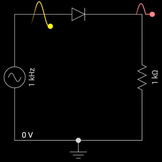
24 During Positive half cycle Anode is at ground potential. Cathode sees variable positive input voltage from o to +V m. For complete positive half cycle diode becomes reverse biased and hence V out = 0V. The circuit and the corresponding output waveform is as shown below During negative half cycle Anode is at ground potential. Cathode sees variable negative input voltage from o to -V m. For complete negative half cycle diode becomes forward biased and hence the output is given as V out = -V m + V k. The circuit and the corresponding output waveform is as shown below Hence applying K.V.L to the loop we have If V in = 10V p p and V K = 0.7V then 24
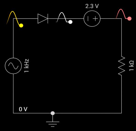
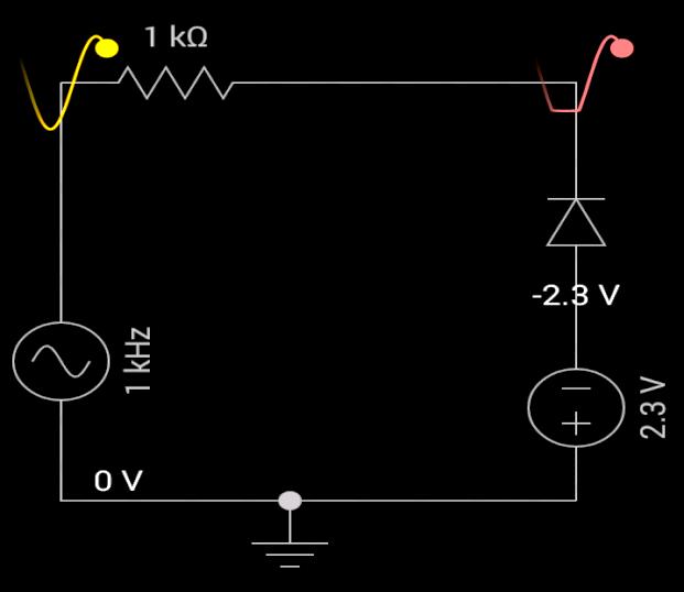
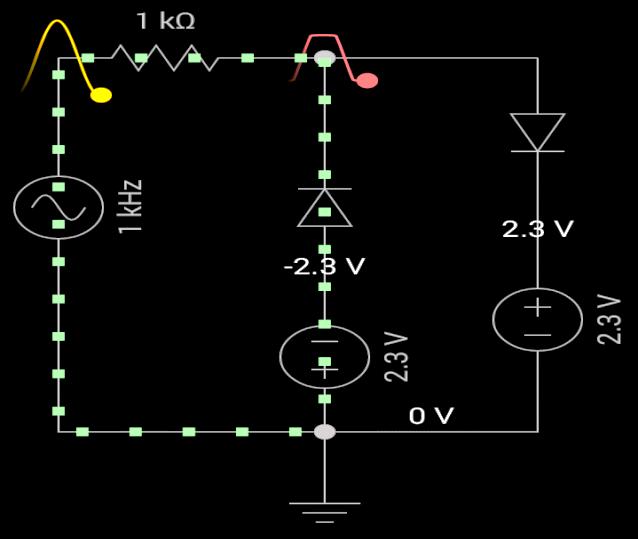
25 2) To pass negative peak above some level say (V R + V k ) During Positive half cycle Anode is at ground potential. Cathode sees variable positive input voltage from V R to V m + V R. For complete positive half cycle diode becomes reverse biased and hence V out = 0V. The circuit and the corresponding output waveform is as shown below During negative half cycle Anode is at ground potential. Cathode sees variable negative input voltage from V R to -V m + V R. When the diode is reverse biased and V o = 0V When the diode is forward biased. The circuit and the corresponding output waveform is as shown below 25
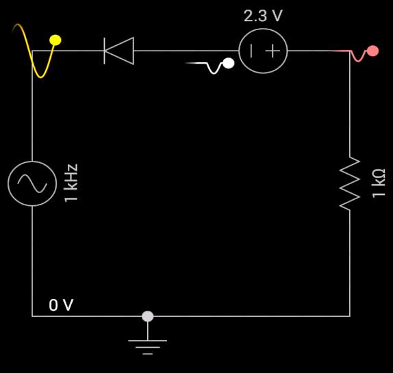
26 Hence applying K.V.L to the loop we have If V in = 10V p p, V K = 0.7V and V R = 2.3V then 3) To pass +ve peak above V K level During Positive half cycle Cathode is at ground potential. Anode sees variable positive input voltage from 0 to +V m. For complete positive half cycle diode becomes forward biased. The circuit and the corresponding output waveform is as shown below If V in = 10V p p, V K = 0.7V 26
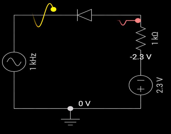
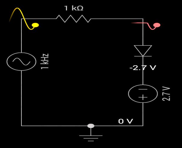
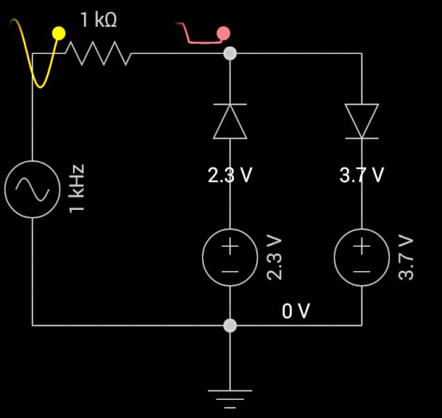
27 During negative half cycle Cathode is at ground potential. Anode sees variable positive input voltage from 0 to -V m. For complete negative half cycle diode becomes reverse biased and hence V out = 0V. The circuit and the corresponding output waveform is as shown below 4) To pass positive peak above some level (V R + V k ) During Positive half cycle Cathode is at ground potential. Anode sees variable positive input voltage from -V R to +V m V R When the diode is reverse biased and V o = 0V When the diode is forward biased. The circuit and the corresponding output waveform is as shown below 27
28 Hence applying K.V.L to the loop we have If V in = 10V p p, V K = 0.7V and V R = 2.3V then During negative half cycle Cathode is at ground potential. Anode sees variable positive input voltage from V R to V m V R For complete negative half cycle diode becomes reverse biased and hence V out = 0V. The circuit and the corresponding output waveform is as shown below Write the output wave form for the following circuit A) Series Clippers 1) 28

29 2) 3) 4) 29

30 5) 6) 7) 30

31 8) 9) 10) 31
 32")
32 11) 12) 13) 32

 2) 33")
33 14) B) Shunt Clippers 1) 2) 33

34 3) 4) 5) 34

35 6) 7) 8) 35
36 9) 10) 36


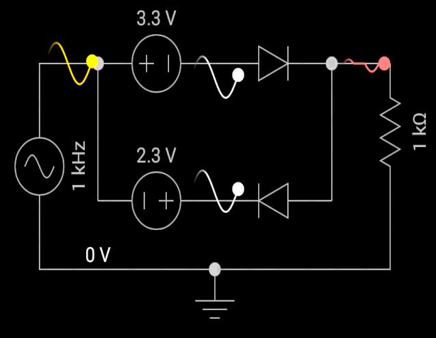
37 1) Sketch the output waveform V o to the time scale Solution Case: 1 for Diodes D1 and D2 are off therefore V o = V i. Case: 2 When Diode D1 conducts and diode D2 is open circuited, Which is as shown in the figure below Applying K.V.L to loops we have 37


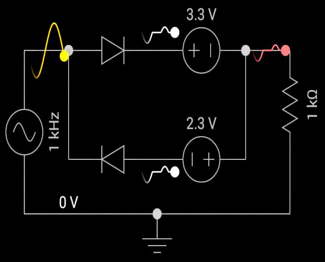
38 Case: 3 When Diodes D1 and D2 are off therefore V o = V i. Case: 4 When Diode D2 conducts and hence Hence the input and output waveform along with transfer characteristics is as shown 2) The input voltage V i to the two level clipper circuit as shown in the figure caries linearly from 0 150V. Sketch the output voltage to time scale. Assume the diodes are ideal. 38


39 Solution: Case: 1 for Diode D1 and D2 are off. The circuit is as sown in figure, Hence Case: 2 for 25V Diodes D1 is off and D2 is on. The circuit is as shown below Applying K.V.L to the loop we have Substituting (1) in and (2) we have [ ] 39


40 Thus for 25V, From equation (3) we have At, At, Case: 3 for 100V Both the diodes becomes on. The circuit is as shown below Apply K.V.L to the above circuit Hence the input and output waveform along with transfer characteristics is as shown 40
41 Clamping circuit Clampers are networks or circuits that changes the input signal to a different DC level but the peak to peak swing of applied signal will remain the same. It adds a DC voltage to the A.C signal hence it is also called as DC restorer DC inserter circuits. The capacitor diode and resistance are the three basic elements of a clamper circuit The clamper circuit relies on a change in the capacitors time constant current path with changing input voltage. The magnitude of R and C are chosen so that T = RC is large enough that the voltage across the capacitor does not discharge significantly during the diodes non conduction state Design: If f = 1KHz T = 1ms Let C = 1μF 1. Positive peak clamped at reference level Capacitor charges only when diode conducts in above circuit diode gets conducted during positive half cycle. When the input voltage is +Ve (V i > 0) the diode is ON and capacitor charges to peak value of input signal as shown in figure 41
42 Apply KV to 1 st loop We know that, Applying K.V.L to 2 nd loop When the input voltage is ve (V i < 0) the diode is OFF as shown in figure Applying KVL Input /output waveform is as shown below 42
43 2) Positive peak clamped at +ve reference (+2V) When diode ON and capacitor starts charging at a very low time constant which is as shown in the figure. Applying KVL to the circuit shown in figure Applying KVL to the second loop Hence 43
44 When the input voltage is ve (V i < 0) the diode is OFF as shown in figure Applying KVL to the circuit shown in figure Input /output waveform is as shown below 3) Positive peak clamped at ve reference level say (-2V) 44
45 When diode ON and capacitor starts charging at a very low time constant Which is as shown in the figure. Applying KVL to the circuit shown in figure Applying KVL to the second loop Hence When the input voltage is ve (V i < 0) the diode is OFF as shown in figure Applying KVL to the circuit shown in figure 45
46 Input /output waveform is as shown below 4) Negative peak clamped level Diode starts conducting during negative half cycle. During this capacitor starts charging to the peak value of the input voltage which is as shown in the figure Apply KV to 1 st loop 46
47 Applying K.V.L to 2 nd loop When the input voltage is +ve (V i > 0) the diode is OFF as shown in figure Applying KVL to the circuit shown in figure Input /output waveform is as shown below 5) Negative peak clamped to +ve reference level (say +2v) 47
48 When input voltage is ve ( shown in figure ) the diode is ON applying KVL to the circuit as Apply KV to 1 st loop Applying KVL to second loop Hence When input is +ve ( >0V) the diode is off applying KVL to circuit in figure Applying KVL to the circuit shown in figure 48
49 Input /output waveform is as shown 6) Negative peak clamped at ve reference level (-2V) When the input voltage is negative (V in < 0) the diode is ON which is as shown in the figure Apply KV to 1 st loop 49
50 Applying KVL to second loop Hence When input is +ve ( >0V) the diode is off applying KVL to circuit in figure Applying KVL to the circuit shown in figure Input /output waveform is as shown 50
51 1) Determine V o for the network as shown in the figure below (ideal diode) Solution Case1: During the interval Diode is ON capacitor charges to peak value of the input signal which is ass shown in the figure Applying K.V.L to the loop1 Applying K.V.L to the loop2 Case2: During the interval Applying K.V.L to the loop 51
52 Case2: During the interval Applying K.V.L to the loop1 Applying K.V.L to the loop2 Input /output waveform is as shown *******END******* 52
Analog Electronic Circuits
 Analog Electronic Circuits Chapter 1: Semiconductor Diodes Objectives: To become familiar with the working principles of semiconductor diode To become familiar with the design and analysis of diode circuits
Chapter 2. Diodes & Applications
 Chapter 2 Diodes & Applications The Diode A diode is made from a small piece of semiconductor material, usually silicon, in which half is doped as a p region and half is doped as an n region with a pn
Clippers limiter circuits Vi > V Vi < V
 Semiconductor Diode Clipper and Clamper Circuits Clippers Clipper circuits, also called limiter circuits, are used to eliminate portion of a signal that are above or below a specified level clip value.
Term Roadmap : Materials Types 1. INSULATORS
 Term Roadmap : Introduction to Signal Processing Differentiating and Integrating Circuits (OpAmps) Clipping and Clamping Circuits(Diodes) Design of analog filters Sinusoidal Oscillators Multivibrators
Basic Electronic Devices and Circuits EE 111 Electrical Engineering Majmaah University 2 nd Semester 1432/1433 H. Chapter 2. Diodes and Applications
 Basic Electronic Devices and Circuits EE 111 Electrical Engineering Majmaah University 2 nd Semester 1432/1433 H Chapter 2 Diodes and Applications 1 Diodes A diode is a semiconductor device with a single
Chapter 1: Diode circuits
 Analog Electronics Circuits Nagamani A N Lecturer, PESIT, Bangalore 85 Email nagamani@pes.edu Chapter 1: Diode circuits Objective To understand the diode operation and its equivalent circuits To understand
Lecture -1: p-n Junction Diode
 Lecture -1: p-n Junction Diode Diode: A pure silicon crystal or germanium crystal is known as an intrinsic semiconductor. There are not enough free electrons and holes in an intrinsic semi-conductor to
Diode Characteristics and Applications
 Diode Characteristics and Applications Topics covered in this presentation: Diode Characteristics Diode Clamp Protecting Against Back-EMF Half-Wave Rectifier The Zener Diode 1 of 18 Diode Characteristics
EC T34 ELECTRONIC DEVICES AND CIRCUITS
 RAJIV GANDHI COLLEGE OF ENGINEERING AND TECHNOLOGY PONDY-CUDDALORE MAIN ROAD, KIRUMAMPAKKAM-PUDUCHERRY DEPARTMENT OF ECE EC T34 ELECTRONIC DEVICES AND CIRCUITS II YEAR Mr.L.ARUNJEEVA., AP/ECE 1 PN JUNCTION
Applications of Diode
 Applications of Diode Diode Approximation: (Large signal operations): 1. Ideal Diode: When diode is forward biased, resistance offered is zero, When it is reverse biased resistance offered is infinity.
UNIT 4 BIASING AND STABILIZATION
 UNIT 4 BIASING AND STABILIZATION TRANSISTOR BIASING: To operate the transistor in the desired region, we have to apply external dec voltages of correct polarity and magnitude to the two junctions of the
Lec (03) Diodes and Applications
 Diodes and Applications") Lec (03) Diodes and Applications Diode Models 1 Diodes and Applications Diode Operation V-I Characteristics of a Diode Diode Models Half-Wave and Full-Wave Rectifiers Power Supply Filters and Regulators
Lec (03) Diodes and Applications Diode Models 1 Diodes and Applications Diode Operation V-I Characteristics of a Diode Diode Models Half-Wave and Full-Wave Rectifiers Power Supply Filters and Regulators
2) The larger the ripple voltage, the better the filter. 2) 3) Clamping circuits use capacitors and diodes to add a dc level to a waveform.
 The larger the ripple voltage, the better the filter. 2) 3) Clamping circuits use capacitors and diodes to add a dc level to a waveform.") TRUE/FALSE. Write 'T' if the statement is true and 'F' if the statement is false. 1) A diode conducts current when forward-biased and blocks current when reverse-biased. 1) 2) The larger the ripple voltage,
TRUE/FALSE. Write 'T' if the statement is true and 'F' if the statement is false. 1) A diode conducts current when forward-biased and blocks current when reverse-biased. 1) 2) The larger the ripple voltage,
Table of Contents. iii
 Table of Contents Subject Page Experiment 1: Diode Characteristics... 1 Experiment 2: Rectifier Circuits... 7 Experiment 3: Clipping and Clamping Circuits 17 Experiment 4: The Zener Diode 25 Experiment
After performing this experiment, you should be able to:
 Objectives: After performing this experiment, you should be able to: Demonstrate the strengths and weaknesses of the two basic rectifier circuits. Draw the output waveforms for the two basic rectifier
KOM2751 Analog Electronics :: Dr. Muharrem Mercimek :: YTU - Control and Automation Dept. 1 1 (CONT D) DIODES
 DIODES") KOM2751 Analog Electronics :: Dr. Muharrem Mercimek :: YTU - Control and Automation Dept. 1 1 (CONT D) DIODES Most of the content is from the textbook: Electronic devices and circuit theory, Robert L.
KOM2751 Analog Electronics :: Dr. Muharrem Mercimek :: YTU - Control and Automation Dept. 1 1 (CONT D) DIODES Most of the content is from the textbook: Electronic devices and circuit theory, Robert L.
A device which removes the peak of a waveform is known as a Clipper. Voltage clipping diagram
 DIODE CLIPPER A device which removes the peak of a waveform is known as a Clipper Voltage clipping diagram Clipping circuit Clipping circuit is a wave-shaping circuit, and is used to either remove or clip
3. Diode, Rectifiers, and Power Supplies
 3. Diode, Rectifiers, and Power Supplies Semiconductor diodes are active devices which are extremely important for various electrical and electronic circuits. Diodes are active non-linear circuit elements
3.4. Reverse Breakdown Region Zener Diodes In the breakdown region Very steep i-v curve Almost constant voltage drop Used for voltage regulator
 3.4. Reverse Breakdown Region Zener Diodes In the breakdown region Very steep i-v curve Almost constant voltage drop Used for voltage regulator Voltage regulator Provide a constant dc output voltage If
semiconductor p-n junction Potential difference across the depletion region is called the built-in potential barrier, or built-in voltage:
 Chapter four The Equilibrium pn Junction The Electric field will create a force that will stop the diffusion of carriers reaches thermal equilibrium condition Potential difference across the depletion
Part I Lectures 1-7 Diode Circuit Applications
 Part Lectures -7 iode Circuit Applications The PN Junction iode Electrical and Electronic Engineering epartment Lecture One - Page of 7 Second Year, Electronics, 9 - The PN Junction iode Basic Construction:
UNIVERSITY OF NORTH CAROLINA AT CHARLOTTE. Department of Electrical and Computer Engineering
 UNIVERSITY OF NORTH CAROLINA AT CHARLOTTE Department of Electrical and Computer Engineering Experiment No. 2 - Semiconductor Diodes Overview: In this lab session students will investigate I-V characteristics
Diodes and Applications
 Diodes and Applications Diodes and Applications 2 1 Diode Operation 2 2 Voltage-Current (V-I) Characteristics 2 3 Diode Models 2 4 Half-Wave Rectifiers 2 5 Full-Wave Rectifiers 2 6 Power Supply Filters
RECTIFIERS AND POWER SUPPLIES
 UNIT V RECTIFIERS AND POWER SUPPLIES Half-wave, full-wave and bridge rectifiers with resistive load. Analysis for Vdc and ripple voltage with C,CL, L-C and C-L-C filters. Voltage multipliers Zenerdiode
3.4. Operation in the Reverse Breakdown
 3.4. peration in the Reverse Breakdown Under certain circumstances, diodes may be intentionally used in the reverse breakdown region These are referred to as Zener Diode or Breakdown Diode Voltage regulator
Diode Limiters or Clipper Circuits
 Diode Limiters or Clipper Circuits Circuits which are used to clip off portions of signal voltages above or below certain levels are called limiters or clippers. Types of Clippers Positive Clipper Negative
Summer 2015 Examination. 1) The answers should be examined by key words and not as word-to-word as given in the model answer scheme.
 The answers should be examined by key words and not as word-to-word as given in the model answer scheme.") Summer 2015 Examination Subject Code: 17215 Model Answer Important Instructions to examiners: 1) The answers should be examined by key words and not as word-to-word as given in the model answer scheme.
Summer 2015 Examination Subject Code: 17215 Model Answer Important Instructions to examiners: 1) The answers should be examined by key words and not as word-to-word as given in the model answer scheme.
Electronic I Lecture 3 Diode Rectifiers. By Asst. Prof Dr. Jassim K. Hmood
 Electronic I Lecture 3 Diode Rectifiers By Asst. Prof Dr. Jassim K. Hmood Diode Approximations 1- The Ideal Model When forward biased, act as a closed (on) switch When reverse biased, act as open (off)
ENG2210 Electronic Circuits. Chapter 3 Diodes
 ENG2210 Electronic Circuits Mokhtar A. Aboelaze York University Chapter 3 Diodes Objectives Learn the characteristics of ideal diode and how to analyze and design circuits containing multiple diodes Learn
The Discussion of this exercise covers the following points:
 Exercise 1 Power Diode Single-Phase Rectifiers EXERCISE OBJECTIVE When you have completed this exercise, you will know what a diode is, and how it operates. You will be familiar with two types of circuits
Circuit operation Let s look at the operation of this single diode rectifier when connected across an alternating voltage source v s.
 Diode Rectifier Circuits One of the important applications of a semiconductor diode is in rectification of AC signals to DC. Diodes are very commonly used for obtaining DC voltage supplies from the readily
Chapter 1: Semiconductor Diodes
 Chapter 1: Semiconductor Diodes Diodes The diode is a 2-terminal device. A diode ideally conducts in only one direction. 2 Diode Characteristics Conduction Region Non-Conduction Region The voltage across
Federal Urdu University of Arts, Science & Technology Islamabad Pakistan SECOND SEMESTER ELECTRONICS - I
 SECOND SEMESTER ELECTRONICS - I BASIC ELECTRICAL & ELECTRONICS LAB DEPARTMENT OF ELECTRICAL ENGINEERING Prepared By: Checked By: Approved By: Engr. Yousaf Hameed Engr. M.Nasim Khan Dr.Noman Jafri Lecturer
EDC Lecture Notes UNIT-1
 P-N Junction Diode EDC Lecture Notes Diode: A pure silicon crystal or germanium crystal is known as an intrinsic semiconductor. There are not enough free electrons and holes in an intrinsic semi-conductor
Electronics 1 Lab (CME 2410) Part I - Diode Clipper
 Part I - Diode Clipper") Electronics 1 Lab (CME 2410) School of Informatics & Computing German Jordanian University Laboratory Experiment (3) Prelab: 1. Simulate the procedure describe in Part I, Section 5d (Negative Polarized
Electronics 1 Lab (CME 2410) School of Informatics & Computing German Jordanian University Laboratory Experiment (3) Prelab: 1. Simulate the procedure describe in Part I, Section 5d (Negative Polarized
1 Diodes. 1.1 Diode Models Ideal Diode. ELEN 236 Diodes
 ELEN 236 Diodes 1 Diodes 1.1 Diode Models 1.1.1 Ideal Diode Current through diode is zero for any voltage less than zero i.e. reverse biased case Current through diode is not limited by diode if voltage
Oscillators. An oscillator may be described as a source of alternating voltage. It is different than amplifier.
 Oscillators An oscillator may be described as a source of alternating voltage. It is different than amplifier. An amplifier delivers an output signal whose waveform corresponds to the input signal but
Electron Devices and Circuits (EC 8353)
") Electron Devices and Circuits (EC 8353) Prepared by Ms.S.KARKUZHALI, A.P/EEE Diodes The diode is a 2-terminal device. A diode ideally conducts in only one direction. Diode Characteristics Conduction Region
Electron Devices and Circuits (EC 8353) Prepared by Ms.S.KARKUZHALI, A.P/EEE Diodes The diode is a 2-terminal device. A diode ideally conducts in only one direction. Diode Characteristics Conduction Region
Lecture (03) Diodes and Diode Applications I
 Diodes and Diode Applications I") Lecture (03) Diodes and Diode Applications I By: Dr. Ahmed ElShafee ١ Agenda VOLTAGE CURRENT CHARACTERISTIC OF A DIODE Forward bias Reverse Bias V I Characteristic for Forward Bias V I Characteristic for
Lecture (03) Diodes and Diode Applications I By: Dr. Ahmed ElShafee ١ Agenda VOLTAGE CURRENT CHARACTERISTIC OF A DIODE Forward bias Reverse Bias V I Characteristic for Forward Bias V I Characteristic for
Diodes (non-linear devices)
") C H A P T E R 4 Diodes (non-linear devices) Ideal Diode Figure 4.2 The two modes of operation of ideal diodes and the use of an external circuit to limit (a) the forward current and (b) the reverse voltage.
C H A P T E R 4 Diodes (non-linear devices) Ideal Diode Figure 4.2 The two modes of operation of ideal diodes and the use of an external circuit to limit (a) the forward current and (b) the reverse voltage.
Diode Bridges. Book page
 Diode Bridges Book page 450-454 Rectification The process of converting an ac supply into dc is called rectification The device that carries this out is called a rectifier Half wave rectifier only half
Chapter #4: Diodes. from Microelectronic Circuits Text by Sedra and Smith Oxford Publishing
 Chapter #4: Diodes from Microelectronic Circuits Text by Sedra and Smith Oxford Publishing Introduction IN THIS CHAPTER WE WILL LEARN the characteristics of the ideal diode and how to analyze and design
Shankersinh Vaghela Bapu Institute of Technology INDEX
 Shankersinh Vaghela Bapu Institute of Technology Diploma EE Semester III 3330905: ELECTRONIC COMPONENTS AND CIRCUITS INDEX Sr. No. Title Page Date Sign Grade 1 Obtain I-V characteristic of Diode. 2 To
EXPERIMENT 2.2 NON-LINEAR OP-AMP CIRCUITS
 2.16 EXPERIMENT 2.2 NONLINEAR OPAMP CIRCUITS 2.2.1 OBJECTIVE a. To study the operation of 741 opamp as comparator. b. To study the operation of active diode circuits (precisions circuits) using opamps,
Intrinsic Semiconductor
 Semiconductors Crystalline solid materials whose resistivities are values between those of conductors and insulators. Good electrical characteristics and feasible fabrication technology are some reasons
IENGINEERS- CONSULTANTS QUESTION BANK SERIES ELECTRONICS ENGINEERING 1 YEAR UPTU
 ELECTRONICS ENGINEERING Unit 1 Objectives Q.1 The breakdown mechanism in a lightly doped p-n junction under reverse biased condition is called. (A) avalanche breakdown. (B) zener breakdown. (C) breakdown
SUMMER 13 EXAMINATION Subject Code: Model Answer Page No: / N
 Important Instructions to examiners: 1) The answers should be examined by key words and not as word-to-word as given in the model answer scheme. 2) The model answer and the answer written by candidate
EXPERIMENT 3 Half-Wave and Full-Wave Rectification
 Name & Surname: ID: Date: EXPERIMENT 3 Half-Wave and Full-Wave Rectification Objective To calculate, compare, draw, and measure the DC output voltages of half-wave and full-wave rectifier circuits. Tools
About the Tutorial. Audience. Prerequisites. Copyright & Disclaimer. Linear Integrated Circuits Applications
 About the Tutorial Linear Integrated Circuits are solid state analog devices that can operate over a continuous range of input signals. Theoretically, they are characterized by an infinite number of operating
EXPERIMENT 5 : DIODES AND RECTIFICATION
 EXPERIMENT 5 : DIODES AND RECTIFICATION Component List Resistors, one of each o 2 1010W o 1 1k o 1 10k 4 1N4004 (Imax = 1A, PIV = 400V) Diodes Center tap transformer (35.6Vpp, 12.6 VRMS) 100 F Electrolytic
Electronic Circuits I - Tutorial 03 Diode Applications I
 Electronic Circuits I - Tutorial 03 Diode Applications I -1 / 13 - T & F # Question 1 A diode can conduct current in two directions with equal ease. F 2 When reverse-biased, a diode ideally appears as
EXPERIMENT 4 LIMITER AND CLAMPER CIRCUITS
 EXPERIMENT 4 LIMITER AND CLAMPER CIRCUITS 1. OBJECTIVES 1.1 To demonstrate the operation of a diode limiter. 1.2 To demonstrate the operation of a diode clamper. 2. INTRODUCTION PART A: Limiter Circuit
EXPERIMENTS USING SEMICONDUCTOR DIODES
 EXPERIMENT 9 EXPERIMENTS USING SEMICONDUCTOR DIODES Semiconductor Diodes Structure 91 Introduction Objectives 92 Basics of Semiconductors Revisited 93 A p-n Junction Operation of a p-n Junction A Forward
CHAPTER 2. Diode Applications
 CHAPTER 2 Diode Applications 1 Objectives Explain and analyze the operation of both half and full wave rectifiers Explain and analyze filters and regulators and their characteristics Explain and analyze
EXPERIMENT 5 : THE DIODE
 EXPERIMENT 5 : THE DIODE Component List Resistors, one of each o 1 10 10W o 1 1k o 1 10k 4 1N4004 (Imax = 1A, PIV = 400V) Diodes Center tap transformer (35.6Vpp, 12.6 VRMS) 100 F Electrolytic Capacitor
EC6202- ELECTRONIC DEVICES AND CIRCUITS UNIT TEST-1 EXPECTED QUESTIONS
 EC6202- ELECTRONIC DEVICES AND CIRCUITS UNIT TEST-1 EXPECTED QUESTIONS 1. List the PN diode parameters. 1. Bulk Resistance. 2. Static Resistance/Junction Resistance (or) DC Forward Resistance 3. Dynamic
The shape of the waveform will be the same, but its level is shifted either upward or downward. The values of the resistor R and capacitor C affect
 Diode as Clamper A clamping circuit is used to place either the positive or negative peak of a signal at a desired level. The dc component is simply added or subtracted to/from the input signal. The clamper
2 MARKS EE2203 ELECTRONIC DEVICES AND CIRCUITS UNIT 1
 2 MARKS EE2203 ELECTRONIC DEVICES AND CIRCUITS UNIT 1 1. Define PN junction. When a p type semiconductor is joined to a N type semiconductor the contact surface is called PN junction. 2. What is an ideal
Chapter Two "Bipolar Transistor Circuits"
 Chapter Two "Bipolar Transistor Circuits" 1.TRANSISTOR CONSTRUCTION:- The transistor is a three-layer semiconductor device consisting of either two n- and one p-type layers of material or two p- and one
EE/COE 152: Basic Electronics. Lecture 3. A.S Agbemenu. https://sites.google.com/site/agbemenu/courses/ee-coe-152
 EE/COE 152: Basic Electronics Lecture 3 A.S Agbemenu https://sites.google.com/site/agbemenu/courses/ee-coe-152 Books: Microelcetronic Circuit Design (Jaeger/Blalock) Microelectronic Circuits (Sedra/Smith)
State the application of negative feedback and positive feedback (one in each case)
") (ISO/IEC - 700-005 Certified) Subject Code: 073 Model wer Page No: / N Important Instructions to examiners: ) The answers should be examined by key words and not as word-to-word as given in the model answer
(ISO/IEC - 700-005 Certified) Subject Code: 073 Model wer Page No: / N Important Instructions to examiners: ) The answers should be examined by key words and not as word-to-word as given in the model answer
PN Junction Diode Table of Contents. What Are Diodes Made Out Of?
 PN Junction iode Table of Contents What are diodes made out of?slide 3 N-type materialslide 4 P-type materialslide 5 The pn junctionslides 6-7 The biased pn junctionslides 8-9 Properties of diodesslides
Lecture (04) Diode applications, cont.
 Diode applications, cont.") Lecture (04) Diode applications, cont. By: Dr. Ahmed ElShafee Agenda Full wave rectifier, cont.,.. Filters Voltage Regulators Diode limiters Diode Clampers ١ ٢ Bridge Full Wave Rectifier Operation uses
Lecture (04) Diode applications, cont. By: Dr. Ahmed ElShafee Agenda Full wave rectifier, cont.,.. Filters Voltage Regulators Diode limiters Diode Clampers ١ ٢ Bridge Full Wave Rectifier Operation uses
Shankersinh Vaghela Bapu Institute of Technology
 Shankersinh Vaghela Bapu Institute of Technology B.E. Semester III (EC) 131101: Basic Electronics INDEX Sr. No. Title Page Date Sign Grade 1 [A] To Study the V-I characteristic of PN junction diode. [B]
DIGITAL ELECTRONICS WAVE SHAPING AND PULSE CIRCUITS. September 2012
 AM 5-403 DIGITAL ELECTRONICS WAVE SHAPING AND PULSE CIRCUITS September 2012 DISTRIBUTION RESTRICTION: Approved for public release. Distribution is unlimited. DEPARTMENT OF THE ARMY MILITARY AUXILIARY RADIO
Electronics I. Midterm #1
 The University of Toledo s6ms_elct7.fm - Electronics I Midterm # Problems Points. 4 2. 5 3. 6 Total 5 Was the exam fair? yes no The University of Toledo s6ms_elct7.fm - 2 Problem 4 points For full credit,
FET Channel. - simplified representation of three terminal device called a field effect transistor (FET)
") FET Channel - simplified representation of three terminal device called a field effect transistor (FET) - overall horizontal shape - current levels off as voltage increases - two regions of operation 1.
FET Channel - simplified representation of three terminal device called a field effect transistor (FET) - overall horizontal shape - current levels off as voltage increases - two regions of operation 1.
Exercise 12. Semiconductors EXERCISE OBJECTIVE DISCUSSION OUTLINE DISCUSSION. Introduction to semiconductors. The diode
 Exercise 12 Semiconductors EXERCISE OBJECTIVE When you have completed this exercise, you will be familiar with the operation of a diode. You will learn how to use a diode to rectify ac voltage to produce
Experiments in Analog Electronics
 Ministry of Higher Education and Scientific Research University of Technology Department of Electrical Engineering Analog Electronics Laboratory Experiments in Analog Electronics By Firas Mohammed Ali
EE70 - Intro. Electronics
 EE70 - Intro. Electronics Course website: ~/classes/ee70/fall05 Today s class agenda (November 28, 2005) review Serial/parallel resonant circuits Diode Field Effect Transistor (FET) f 0 = Qs = Qs = 1 2π
EXPERIMENT 5 : THE DIODE
 EXPERIMENT 5 : THE DIODE Component List Resistors, one of each o 1 10 10W o 1 1k o 1 10k 4 1N4004 (I max = 1A, PIV = 400V) Diodes Center tap transformer (35.6V pp, 12.6 V RMS ) 100 F Electrolytic Capacitor
Ching-Yuan Yang. (symbol) Called breakdown diode or Zener diode, it can be used as voltage regulator. Breakdown voltage V ZK
 Called breakdown diode or Zener diode, it can be used as voltage regulator. Breakdown voltage V ZK") Diodes Read Chapter 3, Section 3.4-3.6, 3.9 Sedra/Smith s Microelectronic Circuits Ching-Yuan Yang National Chung Hsing University Department of Electrical Engineering Zener diode Operate in the reverse
Diodes Read Chapter 3, Section 3.4-3.6, 3.9 Sedra/Smith s Microelectronic Circuits Ching-Yuan Yang National Chung Hsing University Department of Electrical Engineering Zener diode Operate in the reverse
 FINALTERM EXAMINATION Fall 2009 PHY301- Circuit Theory (Session - 2) Time: 120 min Marks: 70 Question No: 1 ( Marks: 1 ) - Please choose one Charge of 2c and 5c will attract each other repel each other
Electronic Devices. Floyd. Chapter 2. Ninth Edition. Electronic Devices, 9th edition Thomas L. Floyd
 Electronic Devices Ninth Edition Floyd Chapter 2 Agenda Diode Circuits and Applications Half-wave Rectifier Full-wave Rectifier Power Supply Filter Power Supply Regulator Diode Limiting Circuits Diode
Diodes & Rectifiers Nafees Ahamad
 Diodes & Rectifiers Nafees Ahamad Asstt. Prof., EECE Deptt, DIT University, Dehradun Website: www.eedofdit.weebly.com 1 Diodes Electronic devices created by bringing together a p-type and n-type region
F.Y. Diploma : Sem. II [DE/EJ/IE/IS/EE/MU/ET/EN/EX] Basic Electronics
![F.Y. Diploma : Sem. II [DE/EJ/IE/IS/EE/MU/ET/EN/EX] Basic Electronics](/thumbs/95/124107511.jpg "F.Y. Diploma : Sem. II [DE/EJ/IE/IS/EE/MU/ET/EN/EX] Basic Electronics") F.Y. Diploma : Sem. II [DE/EJ/IE/IS/EE/MU/ET/EN/EX] Basic Electronics Time: 3 Hrs.] Prelim Question Paper Solution [Marks : 70 Q.1 Attempt any FIE of the following : [10] Q.1(a) Draw the symbols for (i)
F.Y. Diploma : Sem. II [DE/EJ/IE/IS/EE/MU/ET/EN/EX] Basic Electronics Time: 3 Hrs.] Prelim Question Paper Solution [Marks : 70 Q.1 Attempt any FIE of the following : [10] Q.1(a) Draw the symbols for (i)
Analog Electronics circuits
 ANALOG ELECTRONIC CIRCUITS code: IA marks:25 exam marks:100 UNIT 1: Diode Circuits: Diode Resistance, Diode equivalent circuits, Transition and diffusion capacitance, Reverse recovery time, Load line analysis,
Part II. Devices Diode, BJT, MOSFETs
 Part II Devices Diode, BJT, MOSFETs 49 4 Semiconductor Semiconductor The number of charge carriers available to conduct current 1 is between that of conductors and that of insulators. Semiconductor is
55:041 Electronic Circuits
 55:041 Electronic Circuits Chapter 1 & 2 A. Kruger Diode Review, Page-1 Semiconductors licon () atoms have 4 electrons in valence band and form strong covalent bonds with surrounding atoms. Section 1.1.2
SCR- SILICON CONTROLLED RECTIFIER
 SCR- SILICON CONTROLLED RECTIFIER Definition: When a pn junction is added to a junction transistor, the resulting three pn junction device is called a silicon controlled rectifier. SCR can change alternating
Electro - Principles I
 The PN Junction Diode Introduction to the PN Junction Diode Note: In this chapter we consider conventional current flow. Page 11-1 The schematic symbol for the pn junction diode the shown in Figure 1.
1) A silicon diode measures a low value of resistance with the meter leads in both positions. The trouble, if any, is
 A silicon diode measures a low value of resistance with the meter leads in both positions. The trouble, if any, is") 1) A silicon diode measures a low value of resistance with the meter leads in both positions. The trouble, if any, is A [ ]) the diode is open. B [ ]) the diode is shorted to ground. C [v]) the diode is
1) A silicon diode measures a low value of resistance with the meter leads in both positions. The trouble, if any, is A [ ]) the diode is open. B [ ]) the diode is shorted to ground. C [v]) the diode is
Ideal Diode Summary. p-n Junction. Consequently, characteristics curve of the ideal diode is given by. Ideal diode state = OF F, if V D < 0
 Course Contents ELE230 Electronics I http://www.ee.hacettepe.edu.tr/ usezen/ele230/ Dr. Umut Sezen & Dr. Dinçer Gökcen Department of Electrical and Electronic Engineering Hacettepe University and Diode
Homework Assignment 02
 Question 1 (2 points each unless noted otherwise) 1. Is the following circuit an STC circuit? Homework Assignment 02 (a) Yes (b) No (c) Need additional information Answer: There is one reactive element
 http://www.electronics-tutorials.ws/power/triac.html Triac Tutorial and Basic Principles In the previous tutorial we looked at the construction and operation of the Silicon Controlled Rectifier more commonly
FINALTERM EXAMINATION. Spring PHY301- Circuit Theory
 Date 14/2/2013 Eini FINALTERM EXAMINATION Spring 2010 PHY301- Circuit Theory Time: 90 min Marks: 60 Question No: 1 If we connect 3 capacitors in parallel, the combined effect of all these capacitors will
Chapter 8. Field Effect Transistor
 Chapter 8. Field Effect Transistor Field Effect Transistor: The field effect transistor is a semiconductor device, which depends for its operation on the control of current by an electric field. There
Diodes CHAPTER Rectifier Circuits. Introduction. 4.6 Limiting and Clamping Circuits. 4.2 Terminal Characteristics of Junction Diodes 173
 CHAPTER 4 Diodes Introduction 4.1 4.5 Rectifier Circuits 165 The Ideal Diode 166 4.2 Terminal Characteristics of Junction Diodes 173 4.3 Modeling the Diode Forward Characteristic 179 4.4 Operation in the
AE103 ELECTRONIC DEVICES & CIRCUITS DEC 2014
 Q.2 a. State and explain the Reciprocity Theorem and Thevenins Theorem. a. Reciprocity Theorem: If we consider two loops A and B of network N and if an ideal voltage source E in loop A produces current
Mechatronics Chapter 3-1 Semiconductor devices Diode
 MEMS1082 Mechatronics Chapter 3-1 Semiconductor devices Diode Semiconductor: Si Semiconductor N-type and P-type Semiconductors There are two types of impurities: N-type - In N-type doping, phosphorus or
DOWNLOAD PDF POWER ELECTRONICS DEVICES DRIVERS AND APPLICATIONS
 Chapter 1 : Power Electronics Devices, Drivers, Applications, and Passive theinnatdunvilla.com - Google D Download Power Electronics: Devices, Drivers and Applications By B.W. Williams - Provides a wide
Diode conducts when V anode > V cathode. Positive current flow. Diodes (and transistors) are non-linear device: V IR!
 are non-linear device: V IR!") Diodes: What do we use diodes for? Lecture 5: Diodes and Transistors protect circuits by limiting the voltage (clipping and clamping) turn AC into DC (voltage rectifier) voltage multipliers (e.g. double
Diodes: What do we use diodes for? Lecture 5: Diodes and Transistors protect circuits by limiting the voltage (clipping and clamping) turn AC into DC (voltage rectifier) voltage multipliers (e.g. double
Lecture (04) PN Diode applications II
 PN Diode applications II") Lecture (04) PN Diode applications II By: Dr. Ahmed ElShafee ١ Agenda Full wave rectifier, cont.,.. Filters Voltage Regulators ٢ RMS The RMS value of a set of values (or a continuous time waveform) is
Lecture (04) PN Diode applications II By: Dr. Ahmed ElShafee ١ Agenda Full wave rectifier, cont.,.. Filters Voltage Regulators ٢ RMS The RMS value of a set of values (or a continuous time waveform) is
Figure 1 Diode schematic symbol (left) and physical representation (right)
 and physical representation (right)") Page 1/7 Revision 1 20-Jul-10 OBJECTIVES To reinforce the concepts behind diode circuit analysis Verification of diode theory and operation To understand certain diode applications, such as rectification
Page 1/7 Revision 1 20-Jul-10 OBJECTIVES To reinforce the concepts behind diode circuit analysis Verification of diode theory and operation To understand certain diode applications, such as rectification
EXPERIMENT 5 : THE DIODE
 EXPERIMENT 5 : THE DIODE Equipment List Dual Channel Oscilloscope R, 330, 1k, 10k resistors P, Tri-Power Supply V, 2x Multimeters D, 4x 1N4004: I max = 1A, PIV = 400V Silicon Diode P 2 35.6V pp (12.6 V
Ch5 Diodes and Diodes Circuits
 Circuits and Analog Electronics Ch5 Diodes and Diodes Circuits 5.1 The Physical Principles of Semiconductor 5.2 Diodes 5.3 Diode Circuits 5.4 Zener Diode References: Floyd-Ch2; Gao-Ch6; 5.1 The Physical
LABORATORY 8 DIODE CIRCUITS
 LABORATORY 8 DIODE CIRCUITS A solid state diode consists of a junction of either dissimilar semiconductors (pn junction diode) or a metal and a semiconductor (Schottky barrier diode). Regardless of the
BASIC ELECTRONICS ENGINEERING
 BASIC ELECTRONICS ENGINEERING Objective Questions UNIT 1: DIODES AND CIRCUITS 1 2 3 4 5 6 7 8 9 10 11 12 The process by which impurities are added to a pure semiconductor is A. Diffusing B. Drift C. Doping
Examples to Power Supply
 Examples to Power Supply Example-1: A center-tapped full-wave rectifier connected to a transformer whose each secondary coil has a r.m.s. voltage of 1 V. Assume the internal resistances of the diode and
EE 110 Introduction to Engineering & Laboratory Experience Saeid Rahimi, Ph.D. Lab 6 Diodes: Half-Wave and Full-Wave Rectifiers Converting AC to DC
 EE 110 Introduction to Engineering & Laboratory Experience Saeid Rahimi, Ph.D. Lab 6 Diodes: Half-Wave and Full-Wave Rectifiers Converting C to DC The process of converting a sinusoidal C voltage to a