Chapter 2. Diodes & Applications
|
|
|
- Blaze Pope
- 6 years ago
- Views:
Transcription

1 Chapter 2 Diodes & Applications

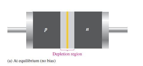
2 The Diode A diode is made from a small piece of semiconductor material, usually silicon, in which half is doped as a p region and half is doped as an n region with a pn junction and depletion region in between.
3 Diode Packages

4 Forward Bias Forward bias is the condition that allows current through the pn junction.

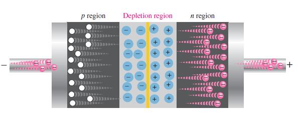
5 Requirements Forward Bias Negative side of VBIAS is connected to the n region of the diode and the positive side is connected to the p region. VBIAS >>> Barrier Potential
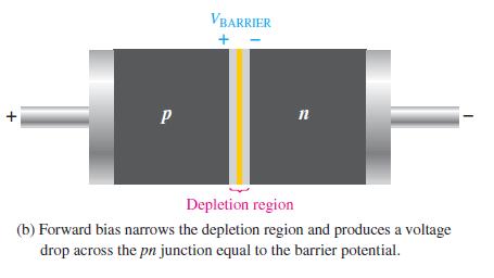
6 Effect of Forward Bias on the Depletion Region As more electrons flow into the depletion region, the number of positive ions is reduced. As more holes effectively flow into the depletion region on the other side of the pn junction, the number of negative ions is reduced. This reduction in positive and negative ions during forward bias causes the depletion region to narrow
7 -cont.
8 Barrier Potential When forward bias is applied, the free electrons are provided with enough energy from the bias-voltage source to overcome the barrier potential and cross the depletion region. The energy that the electrons require in order to pass through the depletion region is equal to the barrier potential. This energy loss results in a voltage drop across the pn junction equal to the barrier potential (0.7 V)

9 Reverse Bias Reverse bias is the condition that essentially prevents current through the diode.
10 -continued
11 Reverse Current The extremely small current that exists in reverse bias after the transition current dies out is caused by the minority carriers in the n and p regions that are produced by thermally generated electron-hole pairs.
12 V-I Characteristic of a Diode
13 V-I Characteristic of a Diode Point A corresponds to a zero-bias condition. Point B corresponds to where the forward voltage is less than the barrier potential of 0.7 V. Point C corresponds to where the forward voltage approximately equals the barrier potential.
14 V-I Characteristic for Reverse Bias
15 The Complete V-I Characteristic Curve
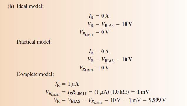
16 Diode Approximations The Ideal Diode Model
17 Diode Approximations The Ideal Diode Model
18 Diode Approximations Since the barrier potential and the forward dynamic resistance are neglected, the diode is assumed to have a zero voltage across it when forward-biased V F = 0 V Forward Current Reverse Current Neglected

19 Diode Approximation Practical Diode Model
20 Diode Approximation Practical Diode Model
21 Diode Approximation Practical Diode Model Applying KVL

22 Diode Approximation Complete Diode Model
23 Diode Approximation Complete Diode Model
24 Diode Approximation Complete Diode Model Formulas

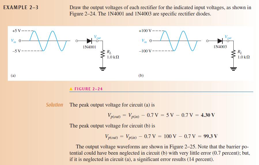
25 Example 2-1
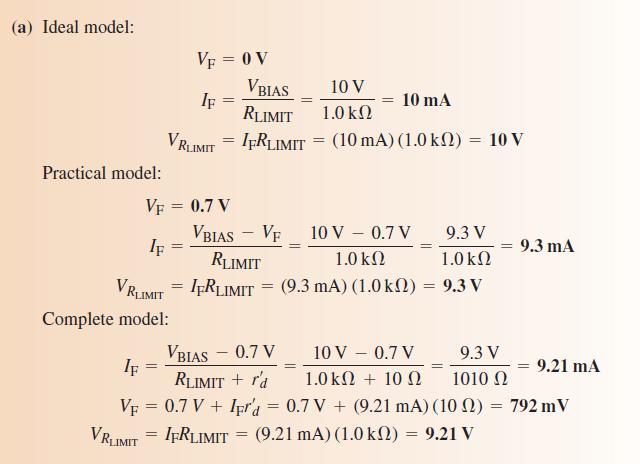
26 Solution
27 Solution
28 Half-wave Rectifiers Because of their ability to conduct current in one direction and block current in the other direction, diodes are used in circuits called rectifiers that convert ac voltage into dc voltage. Rectifiers are found in all dc power supplies that operate from an ac voltage source.
29 Half-wave Rectifiers
30 Half-wave Rectifiers The rectifier converts the ac input voltage to a pulsating dc voltage. The rectifier converts the ac input voltage to a pulsating dc voltage. The regulator is a circuit that maintains a constant dc voltage for variations in the input line voltage or in the load.
31 Half-Wave Rectifier Operation

32 Half-wave Rectifier Average Value of the Half-Wave Output Voltage Example 2-2
33 Effect of Potential Barrier
34

35 Transformer Coupling It allows the source voltage to be stepped down as needed. The ac source is electrically isolated from the rectifier, thus preventing a shock hazard in the secondary circuit.
36 Transformer Coupling Turns Ratio = N sec / N pri Turns Ratio > 1 Step Up Turns Ratio < 1 Step Down Secondary Voltage of Transformer
 current through the load during the entire 360 o of the input")
37 Full-wave Rectifiers A full-wave rectifier allows unidirectional (one-way) current through the load during the entire 360 o of the input cycle.

38 Example 2-5 Full-wave Rectifier
39 Center-Tapped Full-Wave Rectifier Operation
40 Operation
41 Effect of the Turns Ratio on the Output Voltage
42 Effect of the Turns Ratio on the Output Voltage
43 Bridge Full-wave Rectification
44 Bridge Full-wave Rectification
45 Peak Inverse Voltage For rectifier applications, peak inverse voltage (PIV) or peak reverse voltage (PRV) is the maximum value of reverse voltage which occurs at the peak of the input cycle when the diode is reverse-biased.
46 Power Supply Filters & Regulators A power supply filter ideally eliminates the fluctuations in the output voltage of a half-wave or full-wave rectifier and produces a constantlevel dc voltage. A voltage regulator prevents changes in the filtered dc voltage due to variations in input voltage or load.

47 Power Supply Filters & Regulators The small amount of fluctuation in the filter output voltage is called Ripple.
48 Capacitor-Input Filter
49 Capacitor-Input Filter
50 Capacitor-Input Filter

51 Capacitor-Input Filter
52 Ripple Voltage

53 Example 2-8
54 Solution
55 Voltage Regulators
56 Percent Regulation The line regulation specifies how much change occurs in the output voltage for a given change in the input voltage. It is typically defined as a ratio of a change in output voltage for a corresponding change in the input voltage expressed as a percentage.
57 Percent Regulation The load regulation specifies how much change occurs in the output voltage over a certain range of load current values, usually from minimum current (no load, NL) to maximum current (full load, FL).

58 Example 2-9
59 Diode Limiters & Clampers Diode circuits, called limiters or clippers, are sometimes used to clip off portions of signal voltages above or below certain levels. Another type of diode circuit, called a clamper, is used to add or restore a dc level to an electrical signal.
60 Diode Limiters
61 Diode Limiters
62 Biased Limiters
63 Diode Clampers A Clamper adds a dc level to an ac voltage. Operation During the negative half cycle of the input signal, the diode conducts and acts like a short circuit. The output voltage V o 0 volts. The capacitor is charged to the peak value of input voltage V m. and it behaves like a battery. During the positive half of the input signal, the diode does not conduct and acts as an open circuit. Hence the output voltage V o V m + V m This gives a positively clamped voltage.
64 Diode Clampers If the RC time constant is 100 times the period, the clamping action is excellent. An RC time constant of ten times the period will have a small amount of distortion at the ground level due to the charging current.

65 The Diode Datasheet
Basic Electronic Devices and Circuits EE 111 Electrical Engineering Majmaah University 2 nd Semester 1432/1433 H. Chapter 2. Diodes and Applications
 Basic Electronic Devices and Circuits EE 111 Electrical Engineering Majmaah University 2 nd Semester 1432/1433 H Chapter 2 Diodes and Applications 1 Diodes A diode is a semiconductor device with a single
Diodes and Applications
 Diodes and Applications Diodes and Applications 2 1 Diode Operation 2 2 Voltage-Current (V-I) Characteristics 2 3 Diode Models 2 4 Half-Wave Rectifiers 2 5 Full-Wave Rectifiers 2 6 Power Supply Filters
CHAPTER 1 DIODE CIRCUITS. Semiconductor act differently to DC and AC currents
 CHAPTER 1 DIODE CIRCUITS Resistance levels Semiconductor act differently to DC and AC currents There are three types of resistances 1. DC or static resistance The application of DC voltage to a circuit
Lecture (03) Diodes and Diode Applications I
 Diodes and Diode Applications I") Lecture (03) Diodes and Diode Applications I By: Dr. Ahmed ElShafee ١ Agenda VOLTAGE CURRENT CHARACTERISTIC OF A DIODE Forward bias Reverse Bias V I Characteristic for Forward Bias V I Characteristic for
Lecture (03) Diodes and Diode Applications I By: Dr. Ahmed ElShafee ١ Agenda VOLTAGE CURRENT CHARACTERISTIC OF A DIODE Forward bias Reverse Bias V I Characteristic for Forward Bias V I Characteristic for
Electronic Devices. Floyd. Chapter 2. Ninth Edition. Electronic Devices, 9th edition Thomas L. Floyd
 Electronic Devices Ninth Edition Floyd Chapter 2 Agenda Diode Circuits and Applications Half-wave Rectifier Full-wave Rectifier Power Supply Filter Power Supply Regulator Diode Limiting Circuits Diode
Lecture (04) Diode applications, cont.
 Diode applications, cont.") Lecture (04) Diode applications, cont. By: Dr. Ahmed ElShafee Agenda Full wave rectifier, cont.,.. Filters Voltage Regulators Diode limiters Diode Clampers ١ ٢ Bridge Full Wave Rectifier Operation uses
Lecture (04) Diode applications, cont. By: Dr. Ahmed ElShafee Agenda Full wave rectifier, cont.,.. Filters Voltage Regulators Diode limiters Diode Clampers ١ ٢ Bridge Full Wave Rectifier Operation uses
Lecture (04) PN Diode applications II
 PN Diode applications II") Lecture (04) PN Diode applications II By: Dr. Ahmed ElShafee ١ Agenda Full wave rectifier, cont.,.. Filters Voltage Regulators ٢ RMS The RMS value of a set of values (or a continuous time waveform) is
Lecture (04) PN Diode applications II By: Dr. Ahmed ElShafee ١ Agenda Full wave rectifier, cont.,.. Filters Voltage Regulators ٢ RMS The RMS value of a set of values (or a continuous time waveform) is
2) The larger the ripple voltage, the better the filter. 2) 3) Clamping circuits use capacitors and diodes to add a dc level to a waveform.
 The larger the ripple voltage, the better the filter. 2) 3) Clamping circuits use capacitors and diodes to add a dc level to a waveform.") TRUE/FALSE. Write 'T' if the statement is true and 'F' if the statement is false. 1) A diode conducts current when forward-biased and blocks current when reverse-biased. 1) 2) The larger the ripple voltage,
TRUE/FALSE. Write 'T' if the statement is true and 'F' if the statement is false. 1) A diode conducts current when forward-biased and blocks current when reverse-biased. 1) 2) The larger the ripple voltage,
Lecture (03) Diode applications
 Diode applications") Lecture (03) Diode applications By: Dr. Ahmed ElShafee ١ Agenda The Basic DC Power Supply Half wave rectifier Full wave rectifier Filters Voltage Regulators ٢ The Basic DC Power Supply All active electronic
Lecture (03) Diode applications By: Dr. Ahmed ElShafee ١ Agenda The Basic DC Power Supply Half wave rectifier Full wave rectifier Filters Voltage Regulators ٢ The Basic DC Power Supply All active electronic
CHAPTER 2. Diode Applications
 CHAPTER 2 Diode Applications 1 Objectives Explain and analyze the operation of both half and full wave rectifiers Explain and analyze filters and regulators and their characteristics Explain and analyze
Lecture 3 Diodes & Applications :Outline
 Lecture 3 Diodes & Applications :Outline Introduction Diode biasing Diode model Testing a diode Diode application: Rectifiers Diode application: Voltage multipliers Diode application: Optoelectronics 1
Electronic Circuits I - Tutorial 03 Diode Applications I
 Electronic Circuits I - Tutorial 03 Diode Applications I -1 / 13 - T & F # Question 1 A diode can conduct current in two directions with equal ease. F 2 When reverse-biased, a diode ideally appears as
Diode Applications 1
 Diode Applications 1 Explain and analyze the operation of both half and full wave rectifiers Explain and analyze filters and regulators and their characteristics Explain and analyze the operation of diode
RECTIFIERS POWER SUPPLY AND VOLTAGE REGULATION. Rectifier. Basic DC Power Supply. Filter. Regulator
 RECTIFIERS POWER SUPPLY AND OLTAGE REGULATION Prepared by Engr. JP Timola Reference: Electronic Devices by Thomas L. Floyd Because of their ability to conduct current in one direction and block current
Analog Electronic Circuits
 Analog Electronic Circuits Chapter 1: Semiconductor Diodes Objectives: To become familiar with the working principles of semiconductor diode To become familiar with the design and analysis of diode circuits
2 MARKS EE2203 ELECTRONIC DEVICES AND CIRCUITS UNIT 1
 2 MARKS EE2203 ELECTRONIC DEVICES AND CIRCUITS UNIT 1 1. Define PN junction. When a p type semiconductor is joined to a N type semiconductor the contact surface is called PN junction. 2. What is an ideal
Electronic Circuits. Diode Applications. Dr. Manar Mohaisen Office: F208 Department of EECE
 Electronic Circuits Diode Applications Dr. Manar Mohaisen Office: F208 Email: manar.subhi@kut.ac.kr Department of EECE Review of the Precedent Lecture Doping It is a controlled addition of impurities to
Diode Limiters or Clipper Circuits
 Diode Limiters or Clipper Circuits Circuits which are used to clip off portions of signal voltages above or below certain levels are called limiters or clippers. Types of Clippers Positive Clipper Negative
Clippers limiter circuits Vi > V Vi < V
 Semiconductor Diode Clipper and Clamper Circuits Clippers Clipper circuits, also called limiter circuits, are used to eliminate portion of a signal that are above or below a specified level clip value.
Examples to Power Supply
 Examples to Power Supply Example-1: A center-tapped full-wave rectifier connected to a transformer whose each secondary coil has a r.m.s. voltage of 1 V. Assume the internal resistances of the diode and
IENGINEERS- CONSULTANTS QUESTION BANK SERIES ELECTRONICS ENGINEERING 1 YEAR UPTU
 ELECTRONICS ENGINEERING Unit 1 Objectives Q.1 The breakdown mechanism in a lightly doped p-n junction under reverse biased condition is called. (A) avalanche breakdown. (B) zener breakdown. (C) breakdown
Shankersinh Vaghela Bapu Institute of Technology INDEX
 Shankersinh Vaghela Bapu Institute of Technology Diploma EE Semester III 3330905: ELECTRONIC COMPONENTS AND CIRCUITS INDEX Sr. No. Title Page Date Sign Grade 1 Obtain I-V characteristic of Diode. 2 To
Term Roadmap : Materials Types 1. INSULATORS
 Term Roadmap : Introduction to Signal Processing Differentiating and Integrating Circuits (OpAmps) Clipping and Clamping Circuits(Diodes) Design of analog filters Sinusoidal Oscillators Multivibrators
Chapter 1 Introduction to Electronics
 Chapter 1 Introduction to Electronics Section 1-1 Atomic Structure 1. An atom with an atomic number of 6 has 6 electrons and 6 protons.. The third shell of an atom can have n = (3) = 18 electrons. Section
Diode Bridges. Book page
 Diode Bridges Book page 450-454 Rectification The process of converting an ac supply into dc is called rectification The device that carries this out is called a rectifier Half wave rectifier only half
Lecture -1: p-n Junction Diode
 Lecture -1: p-n Junction Diode Diode: A pure silicon crystal or germanium crystal is known as an intrinsic semiconductor. There are not enough free electrons and holes in an intrinsic semi-conductor to
Diodes (non-linear devices)
") C H A P T E R 4 Diodes (non-linear devices) Ideal Diode Figure 4.2 The two modes of operation of ideal diodes and the use of an external circuit to limit (a) the forward current and (b) the reverse voltage.
C H A P T E R 4 Diodes (non-linear devices) Ideal Diode Figure 4.2 The two modes of operation of ideal diodes and the use of an external circuit to limit (a) the forward current and (b) the reverse voltage.
1) A silicon diode measures a low value of resistance with the meter leads in both positions. The trouble, if any, is
 A silicon diode measures a low value of resistance with the meter leads in both positions. The trouble, if any, is") 1) A silicon diode measures a low value of resistance with the meter leads in both positions. The trouble, if any, is A [ ]) the diode is open. B [ ]) the diode is shorted to ground. C [v]) the diode is
1) A silicon diode measures a low value of resistance with the meter leads in both positions. The trouble, if any, is A [ ]) the diode is open. B [ ]) the diode is shorted to ground. C [v]) the diode is
SUMMER 13 EXAMINATION Subject Code: Model Answer Page No: / N
 Important Instructions to examiners: 1) The answers should be examined by key words and not as word-to-word as given in the model answer scheme. 2) The model answer and the answer written by candidate
Analog Electronics. Lecture 3. Muhammad Amir Yousaf
 Analog Electronics Lecture 3 Discrete Semiconductor Devices Rectifier (Diodes) Light Emitting Diodes Zener Diodes Photo Diodes Transistors Bipolar Junction Transistors (BJTs) MOSFETs Diodes A diode is
55:041 Electronic Circuits
 55:041 Electronic Circuits Chapter 1 & 2 A. Kruger Diode Review, Page-1 Semiconductors licon () atoms have 4 electrons in valence band and form strong covalent bonds with surrounding atoms. Section 1.1.2
(A) im (B) im (C)0.5 im (D) im.
 im (B) im (C)0.5 im (D) im.") Dr. Mahalingam College of Engineering and Technology, Pollachi. (An Autonomous Institution affiliated to Anna University) Regulation 2014 Fourth Semester Electrical and Electronics Engineering 141EE0404
Dr. Mahalingam College of Engineering and Technology, Pollachi. (An Autonomous Institution affiliated to Anna University) Regulation 2014 Fourth Semester Electrical and Electronics Engineering 141EE0404
Electronic Circuits I. Instructor: Dr. Alaa Mahmoud
 Electronic Circuits I Instructor: Dr. Alaa Mahmoud alaa_y_emam@hotmail.com Chapter 27 Diode and diode application Outline: Semiconductor Materials The P-N Junction Diode Biasing P-N Junction Volt-Ampere
VTU NOTES QUESTION PAPERS NEWS RESULTS FORUMS TESTING OF HALF WAVE, FULL WAVE AND BRIDGE RECTIFIERS WITH AND WITHOUT CAPACITOR
 TESTING OF HALF WAVE, FULL WAVE AND BRIDGE RECTIFIERS WITH AND WITHOUT CAPACITOR Aim: To determine the ripple factor, efficiency and regulation of the half wave, full wave and bridge rectifier circuits
CHAPTER 5: REGULATED DC POWER SUPPLY
 CHAPTER 5: REGULATED DC POWER SUPPLY Dr. Wan Mahani Hafizah binti Wan Mahmud Topics in Chapter 5 5.0Introduction 5.1Rectifier 5.2Filter 5.3oltage Regulator 5.4Switching Regulator 2 Power Supply Block Diagram
Applications of Diode
 Applications of Diode Diode Approximation: (Large signal operations): 1. Ideal Diode: When diode is forward biased, resistance offered is zero, When it is reverse biased resistance offered is infinity.
Physics 160 Lecture 5. R. Johnson April 13, 2015
 Physics 160 Lecture 5 R. Johnson April 13, 2015 Half Wave Diode Rectifiers Full Wave April 13, 2015 Physics 160 2 Note that there is no ground connection on this side of the rectifier! Output Smoothing
BASIC ELECTRONICS ENGINEERING
 BASIC ELECTRONICS ENGINEERING Objective Questions UNIT 1: DIODES AND CIRCUITS 1 2 3 4 5 6 7 8 9 10 11 12 The process by which impurities are added to a pure semiconductor is A. Diffusing B. Drift C. Doping
A device which removes the peak of a waveform is known as a Clipper. Voltage clipping diagram
 DIODE CLIPPER A device which removes the peak of a waveform is known as a Clipper Voltage clipping diagram Clipping circuit Clipping circuit is a wave-shaping circuit, and is used to either remove or clip
Shankersinh Vaghela Bapu Institute of Technology
 Shankersinh Vaghela Bapu Institute of Technology B.E. Semester III (EC) 131101: Basic Electronics INDEX Sr. No. Title Page Date Sign Grade 1 [A] To Study the V-I characteristic of PN junction diode. [B]
MAHARASHTRA STATE BOARD OF TECHNICAL EDUCATION (Autonomous) (ISO/IEC Certified) Subject Code: Model Answer Page No: 1/
 (ISO/IEC Certified) Subject Code: Model Answer Page No: 1/") MAHARASHTRA STATE BOARD OF TECHNICAL EDUCATION (Autonomous) (ISO/IEC 27001 2005 Certified) SUMMER 13 EXAMINATION Subject Code: 12025 Model Answer Page No: 1/ Important Instructions to examiners: 1) The
MAHARASHTRA STATE BOARD OF TECHNICAL EDUCATION (Autonomous) (ISO/IEC 27001 2005 Certified) SUMMER 13 EXAMINATION Subject Code: 12025 Model Answer Page No: 1/ Important Instructions to examiners: 1) The
Table of Contents. iii
 Table of Contents Subject Page Experiment 1: Diode Characteristics... 1 Experiment 2: Rectifier Circuits... 7 Experiment 3: Clipping and Clamping Circuits 17 Experiment 4: The Zener Diode 25 Experiment
Mechatronics Chapter 3-1 Semiconductor devices Diode
 MEMS1082 Mechatronics Chapter 3-1 Semiconductor devices Diode Semiconductor: Si Semiconductor N-type and P-type Semiconductors There are two types of impurities: N-type - In N-type doping, phosphorus or
 FINALTERM EXAMINATION Fall 2009 PHY301- Circuit Theory (Session - 2) Time: 120 min Marks: 70 Question No: 1 ( Marks: 1 ) - Please choose one Charge of 2c and 5c will attract each other repel each other
3.4. Operation in the Reverse Breakdown
 3.4. peration in the Reverse Breakdown Under certain circumstances, diodes may be intentionally used in the reverse breakdown region These are referred to as Zener Diode or Breakdown Diode Voltage regulator
EXPERIMENT 5 : DIODES AND RECTIFICATION
 EXPERIMENT 5 : DIODES AND RECTIFICATION Component List Resistors, one of each o 2 1010W o 1 1k o 1 10k 4 1N4004 (Imax = 1A, PIV = 400V) Diodes Center tap transformer (35.6Vpp, 12.6 VRMS) 100 F Electrolytic
Scheme I Sample. : Second : Basic. Electronics : 70. Marks. Time: 3 Hrs. 2] b) State any. e) State any. Figure Definition.
![Scheme I Sample. : Second : Basic. Electronics : 70. Marks. Time: 3 Hrs. 2] b) State any. e) State any. Figure Definition.](/thumbs/96/128002629.jpg "Scheme I Sample. : Second : Basic. Electronics : 70. Marks. Time: 3 Hrs. 2] b) State any. e) State any. Figure Definition.") Program Name Program Code Semester Course Title Scheme I Sample Question Paper : Diploma in Electronics Program Group : DE/EJ/IE/IS/ET/EN/EX : Second : Basic Electronics : 70 22216 Time: 3 Hrs. Instructions:
Program Name Program Code Semester Course Title Scheme I Sample Question Paper : Diploma in Electronics Program Group : DE/EJ/IE/IS/ET/EN/EX : Second : Basic Electronics : 70 22216 Time: 3 Hrs. Instructions:
Objective Type Questions 1. Why pure semiconductors are insulators at 0 o K? 2. What is effect of temperature on barrier voltage? 3.
 Objective Type Questions 1. Why pure semiconductors are insulators at 0 o K? 2. What is effect of temperature on barrier voltage? 3. What is difference between electron and hole? 4. Why electrons have
55:041 Electronic Circuits
 55:041 Electronic Circuits Chapter 1 & 2 A. Kruger Diode Review, Page-1 Semiconductors licon () atoms have 4 electrons in valence band and form strong covalent bonds with surrounding atoms. Section 1.1.2
EXPERIMENTS USING SEMICONDUCTOR DIODES
 EXPERIMENT 9 EXPERIMENTS USING SEMICONDUCTOR DIODES Semiconductor Diodes Structure 91 Introduction Objectives 92 Basics of Semiconductors Revisited 93 A p-n Junction Operation of a p-n Junction A Forward
R. W. Erickson. Department of Electrical, Computer, and Energy Engineering University of Colorado, Boulder
 R. W. Erickson Department of Electrical, Computer, and Energy Engineering University of Colorado, Boulder pn junction! Junction diode consisting of! p-doped silicon! n-doped silicon! A p-n junction where
Diode Characteristics and Applications
 Diode Characteristics and Applications Topics covered in this presentation: Diode Characteristics Diode Clamp Protecting Against Back-EMF Half-Wave Rectifier The Zener Diode 1 of 18 Diode Characteristics
Practical Manual. Deptt.of Electronics &Communication Engg. (ECE)
") Practical Manual LAB: BASICS OF ELECTRONICS 1 ST SEM.(CSE/CV) Deptt.of Electronics &Communication Engg. (ECE) RAO PAHALD SINGH GROUP OF INSTITUTIONS BALANA(MOHINDER GARH)12302 Prepared By. Mr.SANDEEP KUMAR
Practical Manual LAB: BASICS OF ELECTRONICS 1 ST SEM.(CSE/CV) Deptt.of Electronics &Communication Engg. (ECE) RAO PAHALD SINGH GROUP OF INSTITUTIONS BALANA(MOHINDER GARH)12302 Prepared By. Mr.SANDEEP KUMAR
1 Diodes. 1.1 Diode Models Ideal Diode. ELEN 236 Diodes
 ELEN 236 Diodes 1 Diodes 1.1 Diode Models 1.1.1 Ideal Diode Current through diode is zero for any voltage less than zero i.e. reverse biased case Current through diode is not limited by diode if voltage
Summer 2015 Examination. 1) The answers should be examined by key words and not as word-to-word as given in the model answer scheme.
 The answers should be examined by key words and not as word-to-word as given in the model answer scheme.") Summer 2015 Examination Subject Code: 17215 Model Answer Important Instructions to examiners: 1) The answers should be examined by key words and not as word-to-word as given in the model answer scheme.
Summer 2015 Examination Subject Code: 17215 Model Answer Important Instructions to examiners: 1) The answers should be examined by key words and not as word-to-word as given in the model answer scheme.
3.4. Reverse Breakdown Region Zener Diodes In the breakdown region Very steep i-v curve Almost constant voltage drop Used for voltage regulator
 3.4. Reverse Breakdown Region Zener Diodes In the breakdown region Very steep i-v curve Almost constant voltage drop Used for voltage regulator Voltage regulator Provide a constant dc output voltage If
Basic Electronics Important questions
 Basic Electronics Important questions B.E-2/4 Mech- B Faculty: P.Lakshmi Prasanna Note: Read the questions in the following order i. Assignment questions ii. Class test iii. Expected questions iv. Tutorials
Electronic I Lecture 3 Diode Rectifiers. By Asst. Prof Dr. Jassim K. Hmood
 Electronic I Lecture 3 Diode Rectifiers By Asst. Prof Dr. Jassim K. Hmood Diode Approximations 1- The Ideal Model When forward biased, act as a closed (on) switch When reverse biased, act as open (off)
Part I Lectures 1-7 Diode Circuit Applications
 Part Lectures -7 iode Circuit Applications The PN Junction iode Electrical and Electronic Engineering epartment Lecture One - Page of 7 Second Year, Electronics, 9 - The PN Junction iode Basic Construction:
EXPERIMENT 5 : THE DIODE
 EXPERIMENT 5 : THE DIODE Component List Resistors, one of each o 1 10 10W o 1 1k o 1 10k 4 1N4004 (Imax = 1A, PIV = 400V) Diodes Center tap transformer (35.6Vpp, 12.6 VRMS) 100 F Electrolytic Capacitor
FINALTERM EXAMINATION. Spring PHY301- Circuit Theory
 Date 14/2/2013 Eini FINALTERM EXAMINATION Spring 2010 PHY301- Circuit Theory Time: 90 min Marks: 60 Question No: 1 If we connect 3 capacitors in parallel, the combined effect of all these capacitors will
CHAPTER 8 The PN Junction Diode
 CHAPTER 8 The PN Junction Diode Consider the process by which the potential barrier of a PN junction is lowered when a forward bias voltage is applied, so holes and electrons can flow across the junction
OBJECTIVE TYPE QUESTIONS FOR PRACTICAL EXAMINATION Subject : Electronics-I ( EC 112)
") OBJECTIVE TYPE QUESTIONS FOR PRACTICAL EXAMINATION Subject : Electronics-I ( EC 112) 1. Which mathematical notation specifies the condition of periodicity for a continuous time signal? a. x(t) = x( t +T)
OBJECTIVE TYPE QUESTIONS FOR PRACTICAL EXAMINATION Subject : Electronics-I ( EC 112) 1. Which mathematical notation specifies the condition of periodicity for a continuous time signal? a. x(t) = x( t +T)
EXPERIMENT 4 LIMITER AND CLAMPER CIRCUITS
 EXPERIMENT 4 LIMITER AND CLAMPER CIRCUITS 1. OBJECTIVES 1.1 To demonstrate the operation of a diode limiter. 1.2 To demonstrate the operation of a diode clamper. 2. INTRODUCTION PART A: Limiter Circuit
Downloaded from
 SOLID AND SEMICONDUCTOR DEVICES (EASY AND SCORING TOPIC) 1. Distinction of metals, semiconductor and insulator on the basis of Energy band of Solids. 2. Types of Semiconductor. 3. PN Junction formation
SUMMER 14 EXAMINATION Model Answer. Subject Code: Page No: 1/
 SUMMER 14 EXAMINATION Model Answer Subject Code: 17215 Page No: 1/ Important Instructions to examiners: 1) The answers should be examined by key words and not as word-to-word as given in the model answer
SCR- SILICON CONTROLLED RECTIFIER
 SCR- SILICON CONTROLLED RECTIFIER Definition: When a pn junction is added to a junction transistor, the resulting three pn junction device is called a silicon controlled rectifier. SCR can change alternating
ชาว ศวกรรมคอมพ วเตอร คณะว ศวกรรมศาสตร มหาว ทยาล ยเทคโนโลย ราชมงคลพระนคร
 EN2042102 วงจรไฟฟ าและอ เล กทรอน กส Circuits and Electronics บทท 6 ไดโอด Diode สาขาว ชาว ศวกรรมคอมพ วเตอร คณะว ศวกรรมศาสตร มหาว ทยาล ยเทคโนโลย ราชมงคลพระนคร Objectives Explain and analyze the operation
EXPERIMENT 7: DIODE CHARACTERISTICS AND CIRCUITS 10/24/10
 DIODE CHARACTERISTICS AND CIRCUITS EXPERIMENT 7: DIODE CHARACTERISTICS AND CIRCUITS 10/24/10 In this experiment we will measure the I vs V characteristics of Si, Ge, and Zener p-n junction diodes, and
THERMIONIC AND GASEOUS STATE DIODES
 THERMIONIC AND GASEOUS STATE DIODES Thermionic and gaseous state (vacuum tube) diodes Thermionic diodes are thermionic-valve devices (also known as vacuum tubes, tubes, or valves), which are arrangements
Lecture 2 p-n junction Diode characteristics. By Asst. Prof Dr. Jassim K. Hmood
 Electronic I Lecture 2 p-n junction Diode characteristics By Asst. Prof Dr. Jassim K. Hmood THE p-n JUNCTION DIODE The pn junction diode is formed by fabrication of a p-type semiconductor region in intimate
Sheet 2 Diodes. ECE335: Electronic Engineering Fall Ain Shams University Faculty of Engineering. Problem (1) Draw the
 Draw the") Ain Shams University Faculty of Engineering ECE335: Electronic Engineering Fall 2014 Sheet 2 Diodes Problem (1) Draw the i) Charge density distribution, ii) Electric field distribution iii) Potential distribution,
Ain Shams University Faculty of Engineering ECE335: Electronic Engineering Fall 2014 Sheet 2 Diodes Problem (1) Draw the i) Charge density distribution, ii) Electric field distribution iii) Potential distribution,
Module 04.(B1) Electronic Fundamentals
 Electronic Fundamentals") 1.1a. Semiconductors - Diodes. Module 04.(B1) Electronic Fundamentals Question Number. 1. What gives the colour of an LED?. Option A. The active element. Option B. The plastic it is encased in. Option
1.1a. Semiconductors - Diodes. Module 04.(B1) Electronic Fundamentals Question Number. 1. What gives the colour of an LED?. Option A. The active element. Option B. The plastic it is encased in. Option
EC6202- ELECTRONIC DEVICES AND CIRCUITS UNIT TEST-1 EXPECTED QUESTIONS
 EC6202- ELECTRONIC DEVICES AND CIRCUITS UNIT TEST-1 EXPECTED QUESTIONS 1. List the PN diode parameters. 1. Bulk Resistance. 2. Static Resistance/Junction Resistance (or) DC Forward Resistance 3. Dynamic
Lesson 5. Electronics: Semiconductors Doping p-n Junction Diode Half Wave and Full Wave Rectification Introduction to Transistors-
 Lesson 5 Electronics: Semiconductors Doping p-n Junction Diode Half Wave and Full Wave Rectification Introduction to Transistors- Types and Connections Semiconductors Semiconductors If there are many free
CENTURION UNIVERSITY OF TECHNOLOGY AND MANAGEMENT SCHOOL OF ENGINEERING & TECHNOLOGYDEPARTMENT OF ELECTRONICS & COMMUNICATION ENGINEERING
 CENTURION UNIVERSITY OF TECHNOLOGY AND MANAGEMENT SCHOOL OF ENGINEERING & TECHNOLOGYDEPARTMENT OF ELECTRONICS & COMMUNICATION ENGINEERING ELECTRONIC DEVICES Section: ECE SEM: II PART-A 1. a) In a N-type
F.Y. Diploma : Sem. II [DE/EJ/IE/IS/EE/MU/ET/EN/EX] Basic Electronics
![F.Y. Diploma : Sem. II [DE/EJ/IE/IS/EE/MU/ET/EN/EX] Basic Electronics](/thumbs/95/124107511.jpg "F.Y. Diploma : Sem. II [DE/EJ/IE/IS/EE/MU/ET/EN/EX] Basic Electronics") F.Y. Diploma : Sem. II [DE/EJ/IE/IS/EE/MU/ET/EN/EX] Basic Electronics Time: 3 Hrs.] Prelim Question Paper Solution [Marks : 70 Q.1 Attempt any FIE of the following : [10] Q.1(a) Draw the symbols for (i)
F.Y. Diploma : Sem. II [DE/EJ/IE/IS/EE/MU/ET/EN/EX] Basic Electronics Time: 3 Hrs.] Prelim Question Paper Solution [Marks : 70 Q.1 Attempt any FIE of the following : [10] Q.1(a) Draw the symbols for (i)
The shape of the waveform will be the same, but its level is shifted either upward or downward. The values of the resistor R and capacitor C affect
 Diode as Clamper A clamping circuit is used to place either the positive or negative peak of a signal at a desired level. The dc component is simply added or subtracted to/from the input signal. The clamper
EXPERIMENT 5 : THE DIODE
 EXPERIMENT 5 : THE DIODE Component List Resistors, one of each o 1 10 10W o 1 1k o 1 10k 4 1N4004 (I max = 1A, PIV = 400V) Diodes Center tap transformer (35.6V pp, 12.6 V RMS ) 100 F Electrolytic Capacitor
IENGINEERS- CONSULTANTS LECTURE NOTES SERIES ELECTRONICS ENGINEERING 1 YEAR UPTU. Lecture-4
 2 P-n Lecture-4 20 Introduction: If a junction is formed between a p-type and a n-type semiconductor this combination is known as p-n junction diode and has the properties of a rectifier 21 Formation of
Wish you all Very Happy New Year
 Wish you all Very Happy New Year Course: Basic Electronics (EC21101) Course Instructors: Prof. Goutam Saha (Sec. 2), Prof. Shailendra K. Varshney (Sec. 1), Prof. Sudip Nag (Sec. 3 ), Prof. Debashish Sen
EE351 Laboratory Exercise 1 Diode Circuits
 revised July 19, 2009 The purpose of this laboratory exercise is to gain experience and understanding working with diodes. Focus on taking good data so that the plots and calculations you will do later
GUJARAT TECHNOLOGICAL UNIVERSITY BE - SEMESTER III EXAMINATION SUMMER 2013
 Seat No.: Enrolment No. GUJARAT TECHNOLOGICAL UNIVERSITY BE - SEMESTER III EXAMINATION SUMMER 2013 Subject Code: 131101 Date: 31-05-2013 Subject Name: Basic Electronics Time: 02.30 pm - 05.00 pm Total
Chapter 2 PN junction and diodes
 Chapter 2 PN junction and diodes ELEC-H402/CH2: PN junction and diodes 1 PN junction and diodes PN junction What happens in a PN junction Currents through the PN junction Properties of the depletion region
Intrinsic Semiconductor
 Semiconductors Crystalline solid materials whose resistivities are values between those of conductors and insulators. Good electrical characteristics and feasible fabrication technology are some reasons
EE70 - Intro. Electronics
 EE70 - Intro. Electronics Course website: ~/classes/ee70/fall05 Today s class agenda (November 28, 2005) review Serial/parallel resonant circuits Diode Field Effect Transistor (FET) f 0 = Qs = Qs = 1 2π
CHAPTER 8 The PN Junction Diode
 CHAPTER 8 The PN Junction Diode Consider the process by which the potential barrier of a PN junction is lowered when a forward bias voltage is applied, so holes and electrons can flow across the junction
Chapter 1: Semiconductor Diodes
 Chapter 1: Semiconductor Diodes Diodes The diode is a 2-terminal device. A diode ideally conducts in only one direction. 2 Diode Characteristics Conduction Region Non-Conduction Region The voltage across
EE/COE 152: Basic Electronics. Lecture 3. A.S Agbemenu. https://sites.google.com/site/agbemenu/courses/ee-coe-152
 EE/COE 152: Basic Electronics Lecture 3 A.S Agbemenu https://sites.google.com/site/agbemenu/courses/ee-coe-152 Books: Microelcetronic Circuit Design (Jaeger/Blalock) Microelectronic Circuits (Sedra/Smith)
WINTER 14 EXAMINATION. Model Answer. Subject Code: ) The answers should be examined by key words and not as word-to-word as given in the
 The answers should be examined by key words and not as word-to-word as given in the") Subject Code: 17215 WINTER 14 EXAMINATION Model Answer Important Instructions to examiners: 1) The answers should be examined by key words and not as word-to-word as given in the model answer scheme. 2)
Subject Code: 17215 WINTER 14 EXAMINATION Model Answer Important Instructions to examiners: 1) The answers should be examined by key words and not as word-to-word as given in the model answer scheme. 2)
جامعة اإلسكندرية كلية الهندسة قسم الهندسة الكهربية أبريل ٢٠١٥
 Alexandria University Faculty of Engineering Electrical Engineering Department April 2015 1a EE 132 Electronic Devices and Circuits First Year Time allowed: 1½ hours جامعة اإلسكندرية كلية الهندسة قسم الهندسة
ELECTRONIC DEVICES AND CIRCUITS 2 Mark Questions Solved UNIT 1
 ELECTRONIC DEVICES AND CIRCUITS 2 Mark Questions Solved UNIT 1 1. What is an ideal diode? An ideal diode is one which offers zero resistance when forward biased and infinite resistance when reverse biased.
Electron Devices and Circuits (EC 8353)
") Electron Devices and Circuits (EC 8353) Prepared by Ms.S.KARKUZHALI, A.P/EEE Diodes The diode is a 2-terminal device. A diode ideally conducts in only one direction. Diode Characteristics Conduction Region
Electron Devices and Circuits (EC 8353) Prepared by Ms.S.KARKUZHALI, A.P/EEE Diodes The diode is a 2-terminal device. A diode ideally conducts in only one direction. Diode Characteristics Conduction Region
FET Channel. - simplified representation of three terminal device called a field effect transistor (FET)
") FET Channel - simplified representation of three terminal device called a field effect transistor (FET) - overall horizontal shape - current levels off as voltage increases - two regions of operation 1.
FET Channel - simplified representation of three terminal device called a field effect transistor (FET) - overall horizontal shape - current levels off as voltage increases - two regions of operation 1.
UNIT 3: FIELD EFFECT TRANSISTORS
 FIELD EFFECT TRANSISTOR: UNIT 3: FIELD EFFECT TRANSISTORS The field effect transistor is a semiconductor device, which depends for its operation on the control of current by an electric field. There are
Class XII - Physics Semiconductor Electronics. Chapter-wise Problems
 lass X - Physics Semiconductor Electronics Materials, Device and Simple ircuit hapter-wise Problems Multiple hoice Question :- 14.1 The conductivity of a semiconductor increases with increase in temperature
Electronics I. Midterm #1
 EECS:3400 Electronics I s5ms_elct7.fm - Section Electronics I Midterm # Problems Points. 4 2. 5 3. 6 Total 5 Was the exam fair? yes no EECS:3400 Electronics I s5ms_elct7.fm - 2 Problem 4 points For full
Lec (03) Diodes and Applications
 Diodes and Applications") Lec (03) Diodes and Applications Diode Models 1 Diodes and Applications Diode Operation V-I Characteristics of a Diode Diode Models Half-Wave and Full-Wave Rectifiers Power Supply Filters and Regulators
Lec (03) Diodes and Applications Diode Models 1 Diodes and Applications Diode Operation V-I Characteristics of a Diode Diode Models Half-Wave and Full-Wave Rectifiers Power Supply Filters and Regulators
Basic Electronics SYLLABUS BASIC ELECTRONICS. Subject Code : 15ELN15/25 IA Marks : 20. Hrs/Week : 04 Exam Hrs. : 03. Total Hrs. : 50 Exam Marks : 80
 SYLLABUS BASIC ELECTRONICS Subject Code : /25 IA Marks : 20 Hrs/Week : 04 Exam Hrs. : 03 Total Hrs. : 50 Exam Marks : 80 Course objectives: The course objective is to make students of all the branches
Lecture 7:PN Junction. Structure, Depletion region, Different bias Conditions, IV characteristics, Examples
 Lecture 7:PN Junction Structure, Depletion region, Different bias Conditions, IV characteristics, Examples PN Junction The diode (pn junction) is formed by dopping a piece of intrinsic silicon, such that