SCR- SILICON CONTROLLED RECTIFIER
|
|
|
- Alexander Strickland
- 6 years ago
- Views:
Transcription
1 SCR- SILICON CONTROLLED RECTIFIER Definition: When a pn junction is added to a junction transistor, the resulting three pn junction device is called a silicon controlled rectifier. SCR can change alternating current into direct current and at the same time can control the amount of power fed to the load. Thus SCR combines the features of a rectifier and a transistor. 1. Invented in 1957, an SCR can be used as a controlled switch to perform various functions 2. Such as rectification, inversion and regulation of power flow. 3. Handle currents upto several thousand amperes and voltages upto more than 1 kv. 4. a unidirectional power switch and is being extensively used in switching d.c. and a.c., rectifying a.c. to give controlled d.c. output, converting d.c. into a.c. 5. A silicon *controlled rectifier is a semiconductor **device that acts as a true electronic switch. Symbol and equivalent circuit Construction 1. It is essentially an ordinary rectifier (pn) and a junction transistor (npn) combined in one unit to form pnpn device. Three terminals are taken; one from the outer p-type material called anode A, 2. Second from the outer n-type material called cathode K and the third from the base of transistor section and is called gate G. 3. In the normal operating conditions of SCR, anode is held at high positive potential w.r.t. cathode and gate at small positive potential w.r.t. cathode. 4. The gate, anode and cathode of SCR correspond to the grid, plate and cathode of thyratron. 5. For this reason, SCR is sometimes called thyristor

2 Equivalent Circuit of SCR Working When gate is open 1. Load is connected in series with anode. 2. The anode is always kept at positive potential w.r.t. cathode. 3. The working of SCR can be studied under the following two heads 1. No voltage applied to the gate. 2. Junction J 2 is reverse biased while junctions J 1 and J 3 are forward biased. 3. Junctions J 1 and J 3 is just as in a npn transistor with base open 4. No current flows through the load R L and the SCR is cut off. 5. If the applied voltage is gradually increased, a stage is reached when reverse biased junction J 2 breaks down.
3 6. The SCR now conducts heavily and is said to be in the ON state. 7. The applied voltage at which SCR conducts heavily without gate voltage is called Breakover voltage. When gate is positive w.r.t. cathode 1. The SCR can be made to conduct heavily at smaller applied voltage by applying a small positive potential to the gate. 2. Now junction J 3 is forward biased and junction J 2 is reverse biased. 3. The electrons from n-type material start mov-ing across junction J 3 towards left whereas holes from p-type towards the right. 4. The electrons from junction J 3 are attracted across junction J 2 and gate current starts flowing. As soon as the gate current flows, anode current increases. 5. The increased anode current in turn makes more electrons available at junction J This process continues and in an extremely small time, junction J 2 breaks down and the SCR starts conducting heavily. 7. Once SCR starts conducting, the gate (the reason for this name is obvious) loses all
4 control. Even if gate voltage is removed, the anode current does not decrease at all. 8. The only way to stop conduction (i.e. bring SCR in off condition) is to reduce the applied voltage to zero. Conclusion notes: a. An SCR has two states i.e. either it does not conduct or it conducts heavily. There is no state in between. Therefore, SCR behaves like a switch. b. There are two ways to turn on the SCR. The first method is to keep the gate open and make the supply voltage equal to the breakover voltage. The second method is to operate SCR with supply voltage less than breakover voltage and then turn it on by means of a small voltage ( typically 1.5 V, 30 ma) applied to the gate. c. Applying small positive voltage to the gate is the normal way to close an SCR because the breakover voltage is usually much greater than supply voltage. d. To open the SCR (i.e. to make it non-conducting ), reduce the supply voltage to zero. Important Terms Breakover voltage It is the minimum forward voltage, gate being open, at which SCR starts conducting heavily i.e. turned on Peak reverse voltage (PRV) It is the maximum reverse voltage (cathode positive w.r.t. anode) that can be applied to an SCR without conducting in the reverse direction. Holding current It is the maximum anode current, gate being open, at which SCR is turned off from ON conditions. Forward current rating It is the maximum anode current that an SCR is capable of passing without destruction. Circuit fusing (I 2 t) rating It is the product of square of forward surge current and the time of duration of the surge i.e.,circuit fusing rating = I 2 t V-I Characteristics of SCR
5 It is the curve between anode-cathode voltage (V) and anode current (I) Of an SCR at constant gate voltage. i)forward characteristics 1. When anode is positive w.r.t. cathode, the curve between V and I is called the forward characteristic. 2. In Fig. OABC is the forward characteristic of SCR at I G = If the supply voltage is increased from zero, a point is reached (point A) when the SCR starts conduct-ing. 4. the voltage across SCR suddenly drops as shown by dotted curve AB and most of supply voltage appears across the load resistance R L. 5. If proper gate current is made to flow, SCR can close at much smaller supply voltage. (ii) Reverse characteristics. 1. When anode is negative w.r.t. cathode, the curve between V and I is known as reverse characteristic. 2. The reverse voltage does come across SCR when it is operated with a.c. supply. 3. If the reverse voltage is gradually increased, at first the anode current remains small (i.e. leakage current) and at some reverse voltage, avalanche breakdown occurs and the SCR starts con-ducting heavily in the reverse direction as shown by the curve DE. 4. This maximum reverse voltage at which SCR starts conducting heavily is known as reverse breakdown voltage. Applications of SCR 1. static contactor 2. Power control. 3. Speed control of d.c. shunt motor. 4. Overlight detector 5. SCR as a Switch 1. SCR turn-on methods. the gate voltage V G is increased upto a minimum value to initiate triggering. This minimum value of gate voltage at which SCR is turned ON is called gate triggering voltage V GT. The resulting gate current is called gate triggering current I GT. Thus to turn on an SCR all that we have to do is to apply positive gate voltage equal to VGT or pass a gate current equal to IGT. (i) D.C. gate trigger circuit.
6 1. When the switch is closed, the gate receives sufficient positive voltage (= V GT ) to turn the SCR on. 2. The resistance R 1 connected in the circuit provides noise suppression and improves the turn-on time. 3. The higher the gate-triggered current, the shorter the turn-on time A.C. trigger circuit. 1. An SCR can also be turned on with positive cycle of a.c. gate current. 2. Fig. (ii) shows During the positive half-cycle of the gate current, at some point I G I GT, the device is turned on. SCR turn-off methods. The SCR turn-off poses more problems than SCR turn-on. It is because once the device is ON, the gate loses all control. There are many methods of SCR turn-off. i) Anode current interruption. When the anode current is reduced below a minimum value called holding current, the SCR turns off. The simple way to turn off the SCR is to open the line switch S (ii) Forced commutation The method of discharging a capacitor in parallel with an SCR to turn off the SCR is called forced commutation. SCR Half-Wave Rectifier 1. One important application of an SCR is the controlled half-wave rectification. 2. Fig (i) shows the circuit of an SCR half-wave rectifier. 3. The a.c. supply to be rectified is supplied through the transformer. 4. The load resistance R L is connected in series with the anode. 5. A variable resistance r is inserted in the gate circuit to control the gate current.

7 1. The a.c. supply to be converted into d.c. supply is applied to the primary of the transformer. Suppose the peak reverse voltage appearing across secondary is less than the reverse breakdown voltage of the SCR. 2. This condition ensures that SCR will not break down during negative half-cycles of a.c. supply. 3. During the negative half-cycles of a.c. voltage appearing across secondary, 4. The SCR does not conduct regardless of the gate voltage. 5. It is because in this condition, anode is negative w.r.t. cathode and also PRV is less than the reverse breakdown voltage. 6. The SCR will conduct during the positive half-cycles provided proper gate current is made to flow. 7. The greater the gate current, the lesser the supply voltage at which SCR is turned ON. 8. The gate current can be changed by the variable resistance r. 9. Suppose that gate current is adjusted to such a value that SCR closes at a positive voltage V 1 which is less than the peak voltage V m. 10. SCR will start conducting when secondary a.c. voltage becomes V 1 in the positive halfcycle. 11. Beyond this, the SCR will continue to conduct till voltage becomes zero at which point it is turned OFF. 12. Again at the start of the next positive half-cycle, SCR will start conducting when secondary voltage becomes V Firing angle is α i.e. at this angle in the positive half-cycle, SCR starts conduction. The conduction angle is φ (= 180 α ). 14. It is worthwhile to distinguish between an ordinary half-wave rectifier and SCR halfwave rectifier.
8 15. Whereas an ordinary half-wave rectifier will conduct full positive half-cycle, an SCR half-wave rectifier can be made to conduct full or part of a positive half-cycle by proper adjustment of gate current. 16. Therefore, an SCR can control power fed to the load and hence the name controlled rectifier. Unijunction Transistor (UJT) It is a three-terminal semiconductor switching device. This device has a unique characteristic that when it is triggered, the emitter current increases regeneratively until it is limited by emitter power supply Construction 1. consists of an n-type silicon bar with an electrical connection on each end. The leads to these connections are called base leads base-one B1 and base two B2 Structure and symbol 1.The emitter is heavily doped having many holes. 2.The n region, is lightly doped. For this reason, the resistance between the base terminals is very high ( 5 to 10 kω) when emitter lead is open.
9 Equivalent Circuit of a UJT 1. R B2 is the resistance of silicon bar between B 2 and the point at which the emitter junction lies. 2. R B1 is the resistance of the bar between B 1 and emitter junction. This resistance is shown variable because its value depends upon the bias voltage across the pn junction. (i) With no voltage applied to the UJT, the inter-base resistance is given by R BB = R B1 + R B2 The value of RBB generally lies between 4 kω and 10 kω. (ii) If a voltage V BB is applied between the bases with emitter open, the voltage will divide up across R B1 and R B2. The ratio V 1 /V BB is called intrinsic stand-off ratio and is represented by Greek letter η. The value of η usually lies between 0.51 and 0.82.
10 Voltage across R B1 = η V BB The voltage η V BB appearing across R B1 reverse biases the diode. Therefore, the emitter current is zero. (iii) positive voltage is applied to the emitter, the diode will become forward biased when input voltage exceeds η VBB by VD, the forward voltage drop across the silicon diode i.e. Where V P = η VBB + VD V P = peak point voltage forward voltage drop across silicon diode VD = (j 0.7 V). Operation 1. When the diode D starts conducting, holes are injected from p-type material to the n- type bar. These holes are swept down towards the terminal B This decreases the resistance between emitter and B 1 (indicated by variable resistance symbol for R B1 ) and hence the internal drop from emitter to B The emitter current now increases regeneratively until it is limited by the emitter power supply The device has normally B 2 positive w.r.t. B If voltage V BB is applied between B 2 and B 1 with emitter open a voltage gradient is established along the n-type bar. 5. Since the emitter is located nearer to B 2, more than **half of V BB appears between the emitter and B The voltage V 1 between emitter and B 1 establishes a reverse bias on the pn junction and the emitter current is cut off. 7. A small leakage current flows from B 2 to emitter due to minority carriers. 8. If a positive voltage is applied at the emitter the pn junction will remain reverse
11 biased so long as the input voltage is less than V If the input voltage to the emitter exceeds V 1, the pn junction becomes *forward biased. 10. Under these conditions, holes are injected from p-type material into the n-type bar. These holes are repelled by positive B 2 terminal and they are attracted towards B 1 terminal of the bar. 11. This accumulation of holes in the emitter to B 1 region results in the decrease of resistance in this section of the bar. 12. The result is that internal voltage drop from emitter to B 1 is decreased and hence the emitter current I E increases. 13. As more holes are injected, a condition of saturation will eventually be reached. 14. At this point, the emitter current is limited by emitter power supply only. The device is now in the ON state. 15. If a negative pulse is applied to the emitter, the pn junction is reverse biased and the emitter current is cut off. The device is then said to be in the OFF state Characteristics of UJT 1. Initially, in the cut-off region, as V E increases from zero, slight leakage current flows from terminal B 2 to the emitter. This current is due to the minority carriers in the reverse biased diode. 2. Above a certain value of V E, forward I E begins to flow, increasing until the peak voltage V P and current I P are reached at point P 3. After the peak point P, an attempt to increase in V E suddenly increase in emitter current I E with a corresponding decrease in V E. 4. a negative resistance portion with increase ini E, V E decreases has a reliable quality.
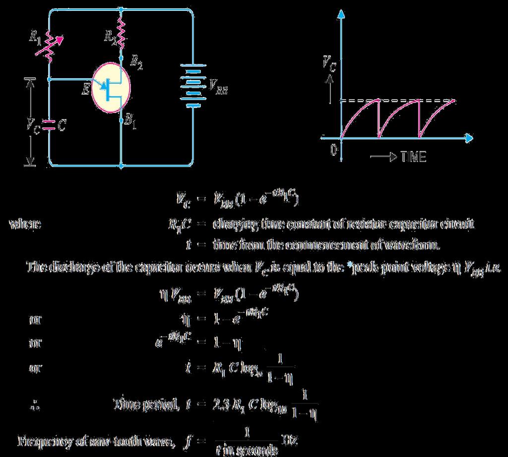
12 5. The negative portion of the curve lasts until the valley point V is reached with valley-point volt-age V V and valley-point current I V. 6. After the valley point, the device is driven to saturation Advantages of UJT (i) It is a low cost device. (ii) It has excellent characteristics. (iii) It is a low-power absorbing device under normal operating conditions Due to above reasons, this device is being used in a variety of applications. A few include oscillators, trigger circuits, saw-tooth generators, bistable network. Applications of UJT i) UJT relaxation oscillator (ii) Overvoltage detector UJT relaxation oscillator- UJT relaxation oscillator where the discharging of a capacitor through UJT can develop a saw-tooth output. 1. When battery V BB is turned on, the capacitor C charges through resistor R During the charging period, the voltage across the capacitor rises in an exponential manner until it reaches the peak - point voltage. 3. At this instant of time, the UJT switches to its low resistance conducting mode and the capacitor is discharged between E and B As the capacitor voltage flys back to zero, the emitter ceases to conduct and the UJT is switched off. 5. The next cycle then begins, allowing the capacitor C to charge again. 6. The frequency of the output saw-tooth wave can be varied by changing the value of R 1 since this controls the time constant R 1 C of the capacitor charging circuit. 7. The time period and hence the frequency of the saw-tooth wave can be calculated as follows. Assuming that the capacitor is initially uncharged, the voltage V C across the capacitor prior to break-down is given by :
13
Unijunction Transistor. T.Y.B.Sc - Eletronics POWER ELETRONICS
 Unijunction Transistor T.Y.B.Sc - Eletronics POWER ELETRONICS Unijunction Transistor Symbol and Construction The Unijunction Transistor is solid state three terminal device that can be used in gate pulse,
BREAKDOWN DEVICES. Learning Objectives
 C H A P T E R64 Learning Objectives What are Breakdown Devices? Unijunction Transistor UJT Relaxation Oscillator Programmable UJT(PUT) Silicon Controlled Rectifier Comparison between Transistors and Thyristors
Basic Electronics Prof. T.S. Natarajan Department of Physics Indian Institute of Technology, Madras
 Basic Electronics Prof. T.S. Natarajan Department of Physics Indian Institute of Technology, Madras Lecture 39 Silicon Controlled Rectifier (SCR) (Construction, characteristics (Dc & Ac), Applications,
UNIT II JFET, MOSFET, SCR & UJT
 UNIT II JFET, MOSFET, SCR & UJT JFET JFET as an Amplifier and its Output Characteristics JFET Applications MOSFET Working Principles, SCR Equivalent Circuit and V-I Characteristics. SCR as a Half wave
IFB270 Advanced Electronic Circuits
 IFB270 Advanced Electronic Circuits Chapter 11: Thyristors Prof. Manar Mohaisen Department of EEC Engineering Review of the Precedent Lecture To introduce several concepts on capacitance in amplifiers
Battery Charger Circuit Using SCR
 Battery Charger Circuit Using SCR Introduction to SCR: SCR is abbreviation for Silicon Controlled Rectifier. SCR has three pins anode, cathode and gate as shown in the below figure. It is made up of there
Oscillators. Hartley, Colpitts, UJT relaxation. ECE/MEA Engg College S.R.K. 9/13/2007 Authored by: Ramesh.K
 Oscillators Hartley, Colpitts, UJT relaxation. S.R.K 9//007 Authored by: Ramesh.K This documents contains a brief note about the principle of sinusoidal oscillator and some general oscillator circuits
Basic Electronics Learning by doing Prof. T.S. Natarajan Department of Physics Indian Institute of Technology, Madras
 Basic Electronics Learning by doing Prof. T.S. Natarajan Department of Physics Indian Institute of Technology, Madras Lecture 38 Unit junction Transistor (UJT) (Characteristics, UJT Relaxation oscillator,
Unijunction Transistor (Volt-Ampere Characteristics)
") Page 1 of 5 Unijunction Transistor (Volt-Ampere Characteristics) Aim :- To draw the volt-ampere characteristics of the unijunction transistor and to find the UJT pameters. Apparatus :- UJT, two variable
Page 1 of 5 Unijunction Transistor (Volt-Ampere Characteristics) Aim :- To draw the volt-ampere characteristics of the unijunction transistor and to find the UJT pameters. Apparatus :- UJT, two variable
 http://www.electronics-tutorials.ws/power/triac.html Triac Tutorial and Basic Principles In the previous tutorial we looked at the construction and operation of the Silicon Controlled Rectifier more commonly
LECTURE NOTES ELECTRONIC CIRCUITS II SYLLABUS
 FATIMA MICHAEL COLLEGE OF ENGINEERING & TECHNOLOGY Madurai Sivagangai Main Road Madurai - 625 020. [An ISO 9001:2008 Certified Institution] LECTURE NOTES EC6401 ELECTRONIC CIRCUITS - II SEMESTER: IV /
UNIT I POWER SEMI-CONDUCTOR DEVICES
 UNIT I POWER SEMI-CONDUCTOR DEVICES SUBJECT CODE SUBJECT NAME STAFF NAME : EE6503 : Power Electronics : Ms.M.Uma Maheswari 1 SEMICONDUCTOR DEVICES POWER DIODE POWER TRANSISTORS POWER BJT POWER MOSFET IGBT
Diodes and Applications
 Diodes and Applications Diodes and Applications 2 1 Diode Operation 2 2 Voltage-Current (V-I) Characteristics 2 3 Diode Models 2 4 Half-Wave Rectifiers 2 5 Full-Wave Rectifiers 2 6 Power Supply Filters
Teccor brand Thyristors AN1001
 A1001 Introduction The Thyristor family of semiconductors consists of several very useful devices. The most widely used of this family are silicon controlled rectifiers (SCRs), Triacs, SIDACs, and DIACs.
Power Semiconductor Devices
 TRADEMARK OF INNOVATION Power Semiconductor Devices Introduction This technical article is dedicated to the review of the following power electronics devices which act as solid-state switches in the circuits.
AE53/AC53/AT53/AE103 ELECT. DEVICES & CIRCUITS DEC 2015
 Q.2 a. By using Norton s theorem, find the current in the load resistor R L for the circuit shown in Fig.1. (8) Fig.1 IETE 1 b. Explain Z parameters and also draw an equivalent circuit of the Z parameter
The silicon controlled rectifier (SCR)
") The silicon controlled rectifier (SCR) Shockley diodes are curious devices, but rather limited in application. Their usefulness may be expanded, however, by equipping them with another means of latching.
The silicon controlled rectifier (SCR) Shockley diodes are curious devices, but rather limited in application. Their usefulness may be expanded, however, by equipping them with another means of latching.
REV NO EXPERIMENT NO 1 AIM: To study the PN junction diode characteristics under Forward & Reverse bias conditions. APPARATUS REQUIRED:
 KARNAL INSTITUTE OF TECHNOLOGY & MANAGEMENT KUNJPURA, KARNAL LAB MANUAL OF ------- SUBJECT CODE DATE OF ISSUE: SEMESTER: BRANCH: REV NO EXPERIMENT NO 1 AIM: To study the PN junction diode characteristics
e base generators Tim 1
 Time base generators 1 LINEAR TIME BASE GENERATORS Circuits thatprovide An Output Waveform Which Exhibits Linear Variation Of Voltage or current With Time. Linear variation of Voltage :Voltage time base
CHADALAWADA RAMANAMMA ENGINEERING COLLEGE (AUTONOMOUS) Chadalawada Nagar, Renigunta Road, Tirupati
 Chadalawada Nagar, Renigunta Road, Tirupati") ELECTRONIC DEVICES AND CIRCUITS LABORATORY MANUAL Subject Code : 17CA04305 Regulations : R17 Class : III Semester (ECE) CHADALAWADA RAMANAMMA ENGINEERING COLLEGE (AUTONOMOUS) Chadalawada Nagar, Renigunta
ELECTRONIC DEVICES AND CIRCUITS LABORATORY MANUAL Subject Code : 17CA04305 Regulations : R17 Class : III Semester (ECE) CHADALAWADA RAMANAMMA ENGINEERING COLLEGE (AUTONOMOUS) Chadalawada Nagar, Renigunta
AN1001. Fundamental Characteristics of Thyristors. Introduction. Basic Operation of a Triac. Basic Operation of an SCR. Basic Operation of a Diac
 A1001 Fundamental Characteristics of Thyristors 14 Introduction The thyristor family of semiconductors consists of several very useful devices. The most widely used of this family are silicon controlled
Solid State Devices- Part- II. Module- IV
 Solid State Devices- Part- II Module- IV MOS Capacitor Two terminal MOS device MOS = Metal- Oxide- Semiconductor MOS capacitor - the heart of the MOSFET The MOS capacitor is used to induce charge at the
UNIT VIII-SPECIAL PURPOSE ELECTRONIC DEVICES. 1. Explain tunnel Diode operation with the help of energy band diagrams.
 UNIT III-SPECIAL PURPOSE ELECTRONIC DEICES 1. Explain tunnel Diode operation with the help of energy band diagrams. TUNNEL DIODE: A tunnel diode or Esaki diode is a type of semiconductor diode which is
Gechstudentszone.wordpress.com
 Unit 1: Transistor, UJT s, and Thyristors In the Diode tutorials we saw that simple diodes are made up from two pieces of semiconductor material, either silicon or germanium to form a simple PN-junction
UNIT 3: FIELD EFFECT TRANSISTORS
 FIELD EFFECT TRANSISTOR: UNIT 3: FIELD EFFECT TRANSISTORS The field effect transistor is a semiconductor device, which depends for its operation on the control of current by an electric field. There are
Chapter 2. Diodes & Applications
 Chapter 2 Diodes & Applications The Diode A diode is made from a small piece of semiconductor material, usually silicon, in which half is doped as a p region and half is doped as an n region with a pn
Prof. Steven S. Saliterman Introductory Medical Device Prototyping
 Introductory Medical Device Prototyping Department of Biomedical Engineering, University of Minnesota http://saliterman.umn.edu/ Solid state power switching: Silicon controlled rectifiers (SCR or Thyristor).
CHAPTER 1 DIODE CIRCUITS. Semiconductor act differently to DC and AC currents
 CHAPTER 1 DIODE CIRCUITS Resistance levels Semiconductor act differently to DC and AC currents There are three types of resistances 1. DC or static resistance The application of DC voltage to a circuit
Diode Limiters or Clipper Circuits
 Diode Limiters or Clipper Circuits Circuits which are used to clip off portions of signal voltages above or below certain levels are called limiters or clippers. Types of Clippers Positive Clipper Negative
Analog Electronic Circuits
 Analog Electronic Circuits Chapter 1: Semiconductor Diodes Objectives: To become familiar with the working principles of semiconductor diode To become familiar with the design and analysis of diode circuits
MAHALAKSHMI ENGINEERING COLLEGE TIRUCHIRAPALLI UNIT V BLOCKING OSCILLATORS AND TIME BASE GENERATORS
 MAHALAKSHMI ENGINEERING COLLEGE TIRUCHIRAPALLI-621213. UNIT V BLOCKING OSCILLATORS AND TIME BASE GENERATORS PART A (2 Marks) 1. What is blocking oscillator? The circuit which uses a regenerative feedback,
SYED AMMAL ENGINEERING COLLEGE
 SYED AMMAL ENGINEERING COLLEGE (Approved by the AICTE, New Delhi, Govt. of Tamilnadu and Affiliated to Anna University, Chennai) Established in 1998 - An ISO 9001:2008 Certified Institution Dr. E.M.Abdullah
CENTURION UNIVERSITY OF TECHNOLOGY AND MANAGEMENT SCHOOL OF ENGINEERING & TECHNOLOGYDEPARTMENT OF ELECTRONICS & COMMUNICATION ENGINEERING
 CENTURION UNIVERSITY OF TECHNOLOGY AND MANAGEMENT SCHOOL OF ENGINEERING & TECHNOLOGYDEPARTMENT OF ELECTRONICS & COMMUNICATION ENGINEERING ELECTRONIC DEVICES Section: ECE SEM: II PART-A 1. a) In a N-type
Reg. No. : Question Paper Code : B.E./B.Tech. DEGREE EXAMINATION, NOVEMBER/DECEMBER Second Semester
 WK 5 Reg. No. : Question Paper Code : 27184 B.E./B.Tech. DEGREE EXAMINATION, NOVEMBER/DECEMBER 2015. Time : Three hours Second Semester Electronics and Communication Engineering EC 6201 ELECTRONIC DEVICES
QUESTION BANK EC6201 ELECTRONIC DEVICES UNIT I SEMICONDUCTOR DIODE PART A. It has two types. 1. Intrinsic semiconductor 2. Extrinsic semiconductor.
 FATIMA MICHAEL COLLEGE OF ENGINEERING & TECHNOLOGY Senkottai Village, Madurai Sivagangai Main Road, Madurai - 625 020. [An ISO 9001:2008 Certified Institution] QUESTION BANK EC6201 ELECTRONIC DEVICES SEMESTER:
Questions on JFET: 1) Which of the following component is a unipolar device?
 Which of the following component is a unipolar device?") Questions on JFET: 1) Which of the following component is a unipolar device? a) BJT b) FET c) DJT d) EFT 2) Current Conduction in FET takes place due e) Majority charge carriers only f) Minority charge
Questions on JFET: 1) Which of the following component is a unipolar device? a) BJT b) FET c) DJT d) EFT 2) Current Conduction in FET takes place due e) Majority charge carriers only f) Minority charge
Dr.Arkan A.Hussein Power Electronics Fourth Class. Commutation of Thyristor-Based Circuits Part-I
 Commutation of Thyristor-Based Circuits Part-I ١ This lesson provides the reader the following: (i) (ii) (iii) (iv) Requirements to be satisfied for the successful turn-off of a SCR The turn-off groups
EDC Lecture Notes UNIT-1
 P-N Junction Diode EDC Lecture Notes Diode: A pure silicon crystal or germanium crystal is known as an intrinsic semiconductor. There are not enough free electrons and holes in an intrinsic semi-conductor
OBJECTIVE TYPE QUESTIONS
 OBJECTIVE TYPE QUESTIONS Q.1 The breakdown mechanism in a lightly doped p-n junction under reverse biased condition is called (A) avalanche breakdown. (B) zener breakdown. (C) breakdown by tunnelling.
UNIT - V POWER DEVICES AND DISPLAY DEVICES
 ISSN (ONLINE) : 2395-695X ISSN (PRINT) : 2395-695X Available online at www.ijarbest.com International Journal of Advanced Research in Biology, Ecology, Science and Technology (IJARBEST) Vol. 1, Issue 9,
IT-T32- Electronic Devices and Circuits UNIT II - SPECIAL DEVICES
 IT-T32- Electronic Devices and Circuits UNIT II - SPECIAL DEVICES SILICON CONTROLLED RECTIFIER (SCR) Introduction The SCR stand for Silicon Control Rectifier, it is used in industries because it can handle
Power Electronics Power semiconductor devices. Dr. Firas Obeidat
 Power Electronics Power semiconductor devices Dr. Firas Obeidat 1 Table of contents 1 Introduction 2 Classifications of Power Switches 3 Power Diodes 4 Thyristors (SCRs) 5 The Triac 6 The Gate Turn-Off
Electronic Circuits I. Instructor: Dr. Alaa Mahmoud
 Electronic Circuits I Instructor: Dr. Alaa Mahmoud alaa_y_emam@hotmail.com Chapter 27 Diode and diode application Outline: Semiconductor Materials The P-N Junction Diode Biasing P-N Junction Volt-Ampere
Emitter base bias. Collector base bias Active Forward Reverse Saturation forward Forward Cut off Reverse Reverse Inverse Reverse Forward
 SEMICONDUCTOR PHYSICS-2 [Transistor, constructional characteristics, biasing of transistors, transistor configuration, transistor as an amplifier, transistor as a switch, transistor as an oscillator] Transistor
SIR PADAMPAT SINGHANIA UNIVERSITY
 SIR PADAMPAT SINGHANIA UNIVERSITY SCHOOL OF ENGINEERING BHATEWAR-3360 ELECTRONIC DEVICES AND CIRCUITS LABORATORY MANUAL DEPARTMENT OF ELECTRONICS & COMMUNICATION ENGINEERING [[ Objective: ) P-N JUNCTION
Lecture 3: Transistors
 Lecture 3: Transistors Now that we know about diodes, let s put two of them together, as follows: collector base emitter n p n moderately doped lightly doped, and very thin heavily doped At first glance,
Diode Characteristics and Applications
 Diode Characteristics and Applications Topics covered in this presentation: Diode Characteristics Diode Clamp Protecting Against Back-EMF Half-Wave Rectifier The Zener Diode 1 of 18 Diode Characteristics
 FINALTERM EXAMINATION Fall 2009 PHY301- Circuit Theory (Session - 2) Time: 120 min Marks: 70 Question No: 1 ( Marks: 1 ) - Please choose one Charge of 2c and 5c will attract each other repel each other
Pre-certification Electronics Questions. Answer the following with the MOST CORRECT answer.
 Electronics Questions Answer the following with the MOST CORRECT answer. 1. The cathode end terminal of a semiconductor diode can be identified by: a. the negative sign marked on the case b. a circular
Power semiconductors. José M. Cámara V 1.0
 Power semiconductors José M. Cámara V 1.0 Introduction Here we are going to study semiconductor devices used in power electronics. They work under medium and high currents and voltages. Some of them only
Transistor Characteristics
 Transistor Characteristics Topics covered in this presentation: Transistor Construction Transistor Operation Transistor Characteristics 1 of 15 The Transistor The transistor is a semiconductor device that
HOW DIODES WORK CONTENTS. Solder plated Part No. Lot No Cathode mark. Solder plated 0.
 www.joeknowselectronics.com Joe Knows, Inc. 1930 Village Center Circle #3-8830 Las Vegas, NV 89134 How Diodes Work Copyright 2013 Joe Knows Electronics HOW DIODES WORK Solder plated 0.4 1.6 There are several
2 Marks - Question Bank. Unit 1- INTRODUCTION
 Two marks 1. What is power electronics? EE6503 POWER ELECTRONICS 2 Marks - Question Bank Unit 1- INTRODUCTION Power electronics is a subject that concerns the applications electronics principles into situations
Switching and Semiconductor Switches
 1 Switching and Semiconductor Switches 1.1 POWER FLOW CONTROL BY SWITCHES The flow of electrical energy between a fixed voltage supply and a load is often controlled by interposing a controller, as shown
Lecture 2 p-n junction Diode characteristics. By Asst. Prof Dr. Jassim K. Hmood
 Electronic I Lecture 2 p-n junction Diode characteristics By Asst. Prof Dr. Jassim K. Hmood THE p-n JUNCTION DIODE The pn junction diode is formed by fabrication of a p-type semiconductor region in intimate
Module 04.(B1) Electronic Fundamentals
 Electronic Fundamentals") 1.1a. Semiconductors - Diodes. Module 04.(B1) Electronic Fundamentals Question Number. 1. What gives the colour of an LED?. Option A. The active element. Option B. The plastic it is encased in. Option
1.1a. Semiconductors - Diodes. Module 04.(B1) Electronic Fundamentals Question Number. 1. What gives the colour of an LED?. Option A. The active element. Option B. The plastic it is encased in. Option
Objective Type Questions 1. Why pure semiconductors are insulators at 0 o K? 2. What is effect of temperature on barrier voltage? 3.
 Objective Type Questions 1. Why pure semiconductors are insulators at 0 o K? 2. What is effect of temperature on barrier voltage? 3. What is difference between electron and hole? 4. Why electrons have
HEATHKIT ELECTRONIC KEYER HD-10
 HEATHKIT ELECTRONIC KEYER HD-10 CIRCUIT DESCRIPTION SCHEMATIC DIAGRAM The letter-number designations on the Schematic Diagram are used to identify resistors, capacitors and diodes. Each designation is
As you can see, by varying the turn-on point, the amount of power getting to the bulb is adjustable, and hence the light output can be controlled.
 Digital Light Dimming Circuit Some light dimmer history Light dimming is based on adjusting the voltage which gets to the lamp. Light dimming has been possible for many decades by using adjustable power
UNIT IV POWER DEVICES
 UNIT IV POWER DEVICES UNI-JUNCTION TRANSISTOR The UJT as the name implies, is characterized by a single pn junction. It exhibits negative resistance characteristic that makes it useful in oscillator circuits.
Silicon Controlled Rectifier
 Page 1 of 5 Silicon Controlled Rectifier Aim :- To draw and study the forward and reverse volt ampere characteristics of the Silicon Controlled Rectifier. Apparatus :- Silicon Controlled Rectifier, voltmeter,
SUMMER 13 EXAMINATION Subject Code: Model Answer Page No: / N
 Important Instructions to examiners: 1) The answers should be examined by key words and not as word-to-word as given in the model answer scheme. 2) The model answer and the answer written by candidate
Q1 A) Attempt any six: i) Draw the neat symbol of N-channel and P-channel FET
 Attempt any six: i) Draw the neat symbol of N-channel and P-channel FET") Subject Code:17319 Model Answer Page1 of 27 Important Instructions to examiners: 1) The answers should be examined by key words and not as word-to-word as given in the model answer scheme. 2) The model
Subject Code:17319 Model Answer Page1 of 27 Important Instructions to examiners: 1) The answers should be examined by key words and not as word-to-word as given in the model answer scheme. 2) The model
Chapter 3 Bipolar Junction Transistors (BJT)
") Chapter 3 Bipolar Junction Transistors (BJT) Transistors In analog circuits, transistors are used in amplifiers and linear regulated power supplies. In digital circuits they function as electrical switches,
Chapter 3 Bipolar Junction Transistors (BJT) Transistors In analog circuits, transistors are used in amplifiers and linear regulated power supplies. In digital circuits they function as electrical switches,
Learn about the use, operation and limitations of thyristors, particularly triacs, in power control
 Exotic Triacs: The Gate to Power Control Learn about the use, operation and limitations of thyristors, particularly triacs, in power control D. Mohan Kumar Modern power control systems use electronic devices
Electrical Engineering EE / EEE. Postal Correspondence Course. Power Electronics. GATE, IES & PSUs
 Power Electronics-EE GATE, IES, PSU 1 SAMPLE STUDY MATERIAL Electrical Engineering EE / EEE Postal Correspondence Course Power Electronics GATE, IES & PSUs Power Electronics-EE GATE, IES, PSU 2 C O N T
Physics 281 EXPERIMENT 7 I-V Curves of Non linear Device
 Physics 281 EXPERIMENT 7 I-V Curves of Non linear Device Print this page to start your lab report (1 copy) Bring a diskette to save your data. OBJECT: To study the method of obtaining the characteristics
Electronics I. Midterm #1
 The University of Toledo s6ms_elct7.fm - Electronics I Midterm # Problems Points. 4 2. 5 3. 6 Total 5 Was the exam fair? yes no The University of Toledo s6ms_elct7.fm - 2 Problem 4 points For full credit,
R a) Draw and explain VI characteristics of Si & Ge diode. (8M) b) Explain the operation of SCR & its characteristics (8M)
 Draw and explain VI characteristics of Si & Ge diode. (8M) b) Explain the operation of SCR & its characteristics (8M)") SET - 1 1. a) Define i) transient capacitance ii) Diffusion capacitance (4M) b) Explain Fermi level in intrinsic and extrinsic semiconductor (4M) c) Derive the expression for ripple factor of Half wave
SET - 1 1. a) Define i) transient capacitance ii) Diffusion capacitance (4M) b) Explain Fermi level in intrinsic and extrinsic semiconductor (4M) c) Derive the expression for ripple factor of Half wave
Lecture -1: p-n Junction Diode
 Lecture -1: p-n Junction Diode Diode: A pure silicon crystal or germanium crystal is known as an intrinsic semiconductor. There are not enough free electrons and holes in an intrinsic semi-conductor to
Field - Effect Transistor
 Page 1 of 6 Field - Effect Transistor Aim :- To draw and study the out put and transfer characteristics of the given FET and to determine its parameters. Apparatus :- FET, two variable power supplies,
Scheme Q.1 Attempt any SIX of following: 12-Total Marks a) Draw symbol NPN and PNP transistor. 2 M Ans: Symbol Of NPN and PNP BJT (1M each)
 Draw symbol NPN and PNP transistor. 2 M Ans: Symbol Of NPN and PNP BJT (1M each)") Q. No. WINTER 16 EXAMINATION (Subject Code: 17319) Model Answer Important Instructions to examiners: 1) The answers should be examined by key words and not as word-to-word as given in the model answer
Q. No. WINTER 16 EXAMINATION (Subject Code: 17319) Model Answer Important Instructions to examiners: 1) The answers should be examined by key words and not as word-to-word as given in the model answer
Subject Code: Model Answer Page No: / N
 Important Instructions to examiners: 1) The answers should be examined by key words and not as word-to-word as given in the model answer scheme. 2) The model answer and the answer written by candidate
Shankersinh Vaghela Bapu Institute of Technology INDEX
 Shankersinh Vaghela Bapu Institute of Technology Diploma EE Semester III 3330905: ELECTRONIC COMPONENTS AND CIRCUITS INDEX Sr. No. Title Page Date Sign Grade 1 Obtain I-V characteristic of Diode. 2 To
The Gate Turn-Off Thyristors (GTO) Part 2
 Part 2") The Gate Turn-Off Thyristors (GTO) Part 2 Static Characteristics On-state Characteristics: In the on-state the GTO operates in a similar manner to the thyristor. If the anode current remains above the
The Gate Turn-Off Thyristors (GTO) Part 2 Static Characteristics On-state Characteristics: In the on-state the GTO operates in a similar manner to the thyristor. If the anode current remains above the
Prepared by: Dr. Rishi Prakash, Dept of Electronics and Communication Engineering Page 1 of 5
 Microwave tunnel diode Some anomalous phenomena were observed in diode which do not follows the classical diode equation. This anomalous phenomena was explained by quantum tunnelling theory. The tunnelling
 SEMICONDUCTOR EECTRONICS MATERIAS, DEVICES AND SIMPE CIRCUITS Important Points: 1. In semiconductors Valence band is almost filled and the conduction band is almost empty. The energy gap is very small
Basic Electronics: Diodes and Transistors. October 14, 2005 ME 435
 Basic Electronics: Diodes and Transistors Eşref Eşkinat E October 14, 2005 ME 435 Electric lectricity ity to Electronic lectronics Electric circuits are connections of conductive wires and other devices
Lecture Switching Characteristics (Dynamic characteristics) Fig. 3.7 : Turn - on characteristics
 Fig. 3.7 : Turn - on characteristics") Lecture-14 3.4 Switching Characteristics (Dynamic characteristics) Thyristor Turn-ON Characteristics Fig. 3.7 : Turn - on characteristics When the SCR is turned on with the application of the gate signal,
Lecture-14 3.4 Switching Characteristics (Dynamic characteristics) Thyristor Turn-ON Characteristics Fig. 3.7 : Turn - on characteristics When the SCR is turned on with the application of the gate signal,
Examples to Power Supply
 Examples to Power Supply Example-1: A center-tapped full-wave rectifier connected to a transformer whose each secondary coil has a r.m.s. voltage of 1 V. Assume the internal resistances of the diode and
Lecture (04) PN Diode applications II
 PN Diode applications II") Lecture (04) PN Diode applications II By: Dr. Ahmed ElShafee ١ Agenda Full wave rectifier, cont.,.. Filters Voltage Regulators ٢ RMS The RMS value of a set of values (or a continuous time waveform) is
Lecture (04) PN Diode applications II By: Dr. Ahmed ElShafee ١ Agenda Full wave rectifier, cont.,.. Filters Voltage Regulators ٢ RMS The RMS value of a set of values (or a continuous time waveform) is
DEPARTMENT OF ECE BAPATLA ENGINEERING COLLEGE BAPATLA
 DEPARTMENT OF ECE BAPATLA ENGINEERING COLLEGE BAPATLA Electronic Devices (EC-251) Lab Manual Prepared by S.Pallaviram, Lecturer T. Srinivasa Rao, Lecturer N.Kusuma, Lab Assistant Department of ECE BEC
ECE 440 Lecture 29 : Introduction to the BJT-I Class Outline:
 ECE 440 Lecture 29 : Introduction to the BJT-I Class Outline: Narrow-Base Diode BJT Fundamentals BJT Amplification Things you should know when you leave Key Questions How does the narrow-base diode multiply
DOWNLOAD PDF POWER ELECTRONICS DEVICES DRIVERS AND APPLICATIONS
 Chapter 1 : Power Electronics Devices, Drivers, Applications, and Passive theinnatdunvilla.com - Google D Download Power Electronics: Devices, Drivers and Applications By B.W. Williams - Provides a wide
Operating Manual Ver.1.1
 UJT Characteristics Operating Manual Ver.1.1 An ISO 9001 : 2000 company 94-101, Electronic Complex Pardesipura, Indore- 452010, India Tel : 91-731- 2570301/02, 4211100 Fax: 91-731- 2555643 e mail : info@scientech.bz
 Electronic Devices 1. Current flowing in each of the following circuits A and respectively are: (Circuit 1) (Circuit 2) 1) 1A, 2A 2) 2A, 1A 3) 4A, 2A 4) 2A, 4A 2. Among the following one statement is not
Chapter 3 Power Electronics 6/13/2009. Electronic Circuit II Chap 3 Power Electronics Silicon Controlled Rectifier
 Electronic Circuit Chap 3 ower Electronics nstructor: jay umar adel athmandu Engineering College Course Homepage www.courses.esmartdesign.com Electronic Circuit 1 ntroduction Thyristor Family SCR Triac
EC T34 ELECTRONIC DEVICES AND CIRCUITS
 RAJIV GANDHI COLLEGE OF ENGINEERING AND TECHNOLOGY PONDY-CUDDALORE MAIN ROAD, KIRUMAMPAKKAM-PUDUCHERRY DEPARTMENT OF ECE EC T34 ELECTRONIC DEVICES AND CIRCUITS II YEAR Mr.L.ARUNJEEVA., AP/ECE 1 PN JUNCTION
Analog & Digital Electronics Course No: PH-218
 Analog & Digital Electronics Course No: PH-218 Lec-5: Bipolar Junction Transistor (BJT) Course nstructors: Dr. A. P. VAJPEY Department of Physics, ndian nstitute of Technology Guwahati, ndia 1 Bipolar
INSTITUTE OF AERONAUTICAL ENGINEERING (AUTONOMOUS) Dundigal, Hyderabad
 Dundigal, Hyderabad") INSTITUTE OF AERONAUTICAL ENGINEERING (AUTONOMOUS) Dundigal, Hyderabad - 500 043 CIVIL ENGINEERING ASSIGNMENT Name : Electrical and Electronics Engineering Code : A30203 Class : II B. Tech I Semester Branch
INSTITUTE OF AERONAUTICAL ENGINEERING (AUTONOMOUS) Dundigal, Hyderabad - 500 043 CIVIL ENGINEERING ASSIGNMENT Name : Electrical and Electronics Engineering Code : A30203 Class : II B. Tech I Semester Branch
Power Electronics. Lecture No - 8
 Power Electronics Prof. B.G. Fernandes Department of Electrical Engineeringg Indian Institute of Technology, Bombay Lecture No - 8 Hello, in my last class we discussed the operation of bipolar junctionn
2 MARKS EE2203 ELECTRONIC DEVICES AND CIRCUITS UNIT 1
 2 MARKS EE2203 ELECTRONIC DEVICES AND CIRCUITS UNIT 1 1. Define PN junction. When a p type semiconductor is joined to a N type semiconductor the contact surface is called PN junction. 2. What is an ideal
WINTER 14 EXAMINATION. Model Answer. 1) The answers should be examined by key words and not as word-to-word as given in the
 The answers should be examined by key words and not as word-to-word as given in the") WINTER 14 EXAMINATION Subject Code: 17213 Model Answer Important Instructions to examiners: 1) The answers should be examined by key words and not as word-to-word as given in the model answer scheme. 2)
WINTER 14 EXAMINATION Subject Code: 17213 Model Answer Important Instructions to examiners: 1) The answers should be examined by key words and not as word-to-word as given in the model answer scheme. 2)
UNIT 3 Transistors JFET
 UNIT 3 Transistors JFET Mosfet Definition of BJT A bipolar junction transistor is a three terminal semiconductor device consisting of two p-n junctions which is able to amplify or magnify a signal. It
Page 1. Date 15/02/2013
 Page 1 Date 15/02/2013 Final Term Examination Fall 2012 Phy301-Circuit Theory 1. State kirchhoff s current law (KCL) Marks: 2: Answer: (PAGE 42) KIRCHHOF S CURRENT LAW Sum of all the currents entering
(a) average output voltage (b) average output current (c) average and rms values of SCR current and (d) input power factor. [16]
![(a) average output voltage (b) average output current (c) average and rms values of SCR current and (d) input power factor. [16]](/thumbs/81/83006678.jpg "(a) average output voltage (b) average output current (c) average and rms values of SCR current and (d) input power factor. [16]") Code No: 07A50204 R07 Set No. 2 1. A single phase fully controlled bridge converter is operated from 230 v, 50 Hz source. The load consists of 10Ω and a large inductance so as to reach the load current
Code No: 07A50204 R07 Set No. 2 1. A single phase fully controlled bridge converter is operated from 230 v, 50 Hz source. The load consists of 10Ω and a large inductance so as to reach the load current
INSTITUTE OF AERONAUTICAL ENGINEERING Dundigal, Hyderabad
 Course Name Course Code Class Branch INSTITUTE OF AERONAUTICAL ENGINEERING Dundigal, Hyderabad -500 043 AERONAUTICAL ENGINEERING TUTORIAL QUESTION BANK : ELECTRICAL AND ELECTRONICS ENGINEERING : A40203
The shape of the waveform will be the same, but its level is shifted either upward or downward. The values of the resistor R and capacitor C affect
 Diode as Clamper A clamping circuit is used to place either the positive or negative peak of a signal at a desired level. The dc component is simply added or subtracted to/from the input signal. The clamper
Semiconductor analyser AS4002P User Manual
 Semiconductor analyser AS4002P User Manual Copyright Ormelabs (C) 2010 http://www.ormelabs.com 1 CONTENTS SECTION Page SECTION 1: Introduction... 3 SECTION 2: Features... 3 SECTION 3: Component analysis...
Physics 160 Lecture 5. R. Johnson April 13, 2015
 Physics 160 Lecture 5 R. Johnson April 13, 2015 Half Wave Diode Rectifiers Full Wave April 13, 2015 Physics 160 2 Note that there is no ground connection on this side of the rectifier! Output Smoothing