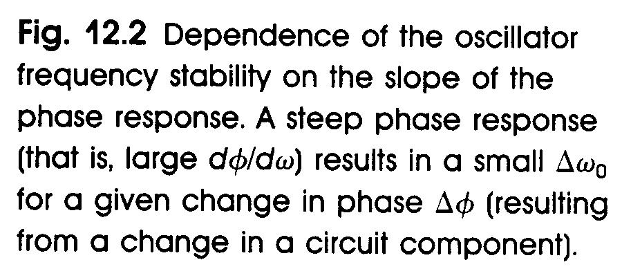
The steeper the phase shift as a function of frequency φ(ω) the more stable the frequency of oscillation
|
|
|
- Franklin Griffin
- 5 years ago
- Views:
Transcription
1 It should be noted that the frequency of oscillation ω o is determined by the phase characteristics of the feedback loop. the loop oscillates at the frequency for which the phase is zero The steeper the phase shift as a function of frequency φ(ω) the more stable the frequency of oscillation
2
3 Non-linear Amplitude Control Generally difficult to design circuits with Aβ = 1 as circuit parameters vary with temperature, time and component values If Aβ < 1 Oscillation ceases If Aβ > 1 Oscillations grow until circuit saturates Require mechanism to force Aβ = 1 this is accomplished by a nonlinear circuit for gain control Design circuit with Aβ > 1 as voltage of oscillation increases gain control mechanism kicks in and reduces gain to 1 Design circuit with right half plane poles. Gain control pulls the poles back to the imaginary axis Two approaches. The first approach uses a limiter circuit, oscillations are allowed to grow until the level reaches the limiter set value. Once the limiter comes into operation, the amplitude remains constant. The limiter should be designed to minimize nonlinear distortion The second method uses a resistive element in the feedback loop whose resistance can be controlled by the sinusoidal output amplitude. Diodes or JFETs (operating in triode region) are commonly used
4 A popular limiter circuit for amplitude control can be seen below:
5
6 Wien - Bridge Oscillator Opamp - RC Oscillators
7 The loop gain can be found by multplying the transfer function of the feedback path v a (s) / v o (s) by the amplifier gain L( s) = 1 + R R 2 1 Z p Z p + Z s L( jω) = R 1+ 2 R1 3+ j ωcr 1 ωcr The loop gain will be a real number (i.e. the phase will be zero) at one frequency given by ω ω ο ο CR = = 1 ω 1 CR ο CR To obtain sustained oscillations at this frequency the magnitude of the loop gain should be unity which can be achieved by setting R2 R 1 = 2
8 To ensure that oscillation starts, one chooses R 2 / R 1 slightly greater than 2 The amplitude of oscillation can be controlled using a non-linear limiter as seen below
9
10 Phase Shift Oscillator The basic structure of the phase shift oscillator is shown below. It consists of a negative gain amplifier (- k) with a three section (third - order) RC ladder network in the feedback
11 The circuit will oscillate at the frequency for which the phase shift of the RC network is 180 o. Only at this frequency will the phase shift around the loop be 0 o (360 o ). Three RC sections are required to produce a 180 o phase shift at a finite frequency The value of k is chosen to be slightly higher than the inverse of the magnitude of the RC network transfer function at the frequency of oscillation
12
13 Active Filter Tuned Oscillator
14
15 The opamp RC oscillator circuits are useful for operation in the 10 Hz - 1 MHz range due to limitations in passive component size (Low frequency) and opamp slew rate (high frequency) for higher frequencies, circuits that employ transistors together with LC tuned circuits or crystals are commonly used
16 LC and Crystal Oscillators Oscillators utilizing transistors and LC tuned circuits or crystals are useful for operation in the range from 100 khz to 500 MHz. They exhibit higher Q than RC types (more stable), however, LC oscillators are difficult to tune over wide ranges and crystal oscillators operate at a single frequency. The extremely stable response of crystal oscillators has made them very popular particularly for digital timing signals
17 t v = L ( L β L ) e τ τ = C R + + substituting v = β L at t = T gives + L 1 β L+ T 1 = τ ln 1 β 1 Similarly for the discharge cycle it can be shown L 1 β + L T 2 = τ ln 1 β If L = L and T = T +T Then T = τ ln 1 β β The square wave generator can be made to have variable frequency by adjusting C and/or R The waveform across C can be made almost triangular by using a small value for the parameter β
18 Phase Lock Loops (PLLs) Useful building block available from numerous vendors as a single IC. Contains a phase detector, low pass filter, amplifier and VCO. Combines digital and analog techniques Applications include tone decoding, demodulating AM and FM signals, frequency multiplication and synthesis and synchronization of signals from noisy sources
19 Phase Lock Loop Block Diagram
20 Phase detector compares two frequencies and generates an output which is a measure of their phase difference The phase error is filtered and amplified and causes the VCO frequency to deviate in the direction of f IN If conditions are right the VCO will quickly lock to f IN maintaining a fixed phase relationship with the input signal When locked the PLL control voltage is a DC signal which is a measure of the input frequency (Tone Decoding, FM Decoding) The VCO output is a locally generated signal and thus provides a clean replica of f IN which may itself be noisy If a modulo N counter is inserted between the VCO and phase detector the VCO will generate a multiple of the input frequency (high speed clocks, power line suppression)
21
22 Phase Detection Two types (Type I & Type II). Type I can be driven by analog or digital (square-wave) signal. Type II is driven by digital transitions (edges) Simplest Type I (digital) is an exclusive OR gate. Type I (linear) has similar output but uses a four quadrant analog multiplier instead of an XOR Type II phase detector is sensitive only to the relative timing edges of the input signal and the VCO output Type II detector is independent of duty cycle. Type I like 50% duty cycle Type I phase detectors always generate an output wave. This results in a small amount of residual ripple and periodic phase modulation (i.e. the VCO output is distorted with phase modulation sidebands) Type II phase detector sensitive to noise
23
24
25
26
27
28 VCO Many PLL s contain an internal VCO. External VCO ICs are also available Some VCOs offer multiple output waveforms such as sine, square and triangle waves (8038, 2206)
29 PLL Design PLLs can be treated as negative feedback amplifiers with one difference. In feedback amplifiers the quantity adjusted is the same quantity measured (commonly). In a phase lock loop we measure phase and adjust frequency. Since phase is an integral of frequency this introduces a 90 o phase shift To avoid oscillation we must insure that further phase shifts in the loop do not cause a 180 o phase at any frequency One solution is to eliminate any further phase shifting components by eliminating the low pass filter. This is referred to as a first order loop First order PLLs are useful, however, they do not allow the VCO to smooth out noise or fluctuations on the input signal A second order PLL has low-pass filtering within the feedback loop carefully designed to prevent instabilities Low-pass filtering provides flywheel memory action which maintains lock even when there are small noise and signal fluctuations Low-pass filtering increases capture time and reduces capture range
30 Second order loops are almost always used PLL design is based on selecting a loop filter and amp which passes the maximum signal frequency you are capturing and reduces the loop gain to less than 1 at 180 o phase shift The loop gain includes the gain of the phase detector, LP filter, amp and VCO VCO acts as integrator with 20 db / decade rolloff and -90 o phase shift K LOOP = K P K F K VCO
31 Generation of Triangle Waveforms The exponential waveform generated in the astable circuit can be changed to triangular by replacing the low-pass RC circuit with an integrator The integrator causes linear charging and discharging of the capacitor. Because the integrator is inverting it is necessary to use the non-inverting bistable circuit V V T L+ T C R V = V 1 = C R L TH TL TH TL 1 + V V T L = T C R V V 2 = C R L TH TL TH TL 2 If L = -L then symmetrical waveforms are obtained + -
32
33
34 Monostable Multivibrators In some applications the need arises for a pulse of known height and width generated in response to a trigger signal Because the width of the pulse is predictable its trailing edge can be used for timing purposes, such a pulse can be generated by a monostable multivibrator The monostable multivibrator has one stable state in which it can remain indefinitely. It also has a quasi-stable state in which it remains for a predetermined interval equal to the desired width of the output pulse Once the interval expires, the monostable returns to the stable state and remains there awaiting another triggering signal. The circuit is commonly called a one shot A monostable circuit is shown below which is an augmented form of the astable circuit
35
36 The duration T of the output pulse is determined by the exponential waveform at v B B ( ) = ( D1 ) v t L L V e t C R 1 3 by substituting β v ( T) = β L ( D1 ) L = L L V e B T C R 1 3 T = C R 1 3 VD1 L ln β L L For V << L This equation can be approximated by T D1 C R ln 1 β Note: The monostable should not be retriggered again until C 1 has been recharged to V D1 (Recovery period)
37 Integrated Circuit Timers Commercially available integrated circuit packages contain the bulk of the circuitry needed to implement monostable and astable multivibrators having precise characteristics. The most popular of such ICs is the 555 timer
38

39 vc = V CC 1 e t RC 2 vc = vth = VCC at t = T 3 T = CRln CR
40
41
42 The rise in v is given by C ( ) v = V V V e C C C C C T L t C R ( + R ) 2 1 v = V = V at t = T ; V = V 3 3 C T H C C H T L CC ( ) ln ( ) T = C R + R C R + R H A B A B A B The fall in v is given by v = V e C T H C t C R v = V 1 2 = V, V = V 3 3 at t = T T = C R ln 2 = 0. 69C R C T L C C T H C C L L B B ( ) T = T + T = C R + 2 R B H L A B
43 LC Tuned Oscillator Two commonly used configurations are the Colpitts and Hartley oscillators. The basic circuit structures without biasing can be seen below
44 Both circuits utilize a parallel LC circuit connected between the collector and base with a fraction of the tuned circuit voltage fed to the emitter The resistor R models the losses of the inductor, the load resistance of the oscillator and the output resistance of the transistor If the frequency of operation is sufficiently low that we can neglect the transistor capacitances, the frequency of oscillation is determined by the resonant frequency of the parallel tuned circuit (also known as a tank circuit) for the Colpitts oscillator ω ο = L C C C + C 1 2 For the Hartley oscillator ω ο = 1 ( + ) L L C 1 2 The ratio L 1 / L 2 or C 1 / C 2 determines the feedback factor and thus must be adjusted in conjunction with the transistor gain to ensure that oscillations will start
45 To determine the oscillation condition for the Colpitts oscillator we replace the transistor with its equivalent circuit To simplify the analysis we neglect the transistor capacitance C µ. Capacitance C π can be considered part of C 2. r π is neglected assuming that r π >> 1 / ω o C 2
46
47 A node equation at the transistor collector (c) yields sc v 2 ( 2 ) 1 + gmv + + sc 1+ s LC v = 0 R 2 π π 1 π since v π 0 (oscillations have started) it can be eliminated ( ) ( ) ( ) 2 / 1 2 m 3 2 s LC1C 2 + s LC R + s C + C + g + 1 R = 0 g m 2 1 ω LC2 [ j ω ( C C ) LC C ] ω 1 2 = 0 R R For oscillations to start both the real and imaginary parts must be zero. Setting the imaginary part to zero gives ω ο = L C C C + C 1 2 which is the resonant frequency of the tank circuit setting the real part to zero gives C2 C = g R 1 m
48 For sustained oscillation the magnitude of the gain from the base to collector (g m R) must be equal to the inverse of the voltage ratio provided by the capacitive divider vbe C v = ce 2 C1 for the oscillation to start the loop gain must be greater than unity which is equivalent to g R C C m > 2 1 As oscillations grow in amplitude, the transistor s non-linear characteristics reduce the loop gain to unity, thus sustaining oscillations An example of a complete Colpitts oscillator is shown on the next page
49
50 The radio frequency choke (RFC) provides a high reactance at ω o but a low DC resistance Unlike the opamp oscillators that incorporate special amplitude control circuitry, LC tuned oscillators utilize the non-linear i C - v BE characteristics of the BJT (or i D versus v GS for FETs) for amplitude control. As the oscillations grow the effective gain of the transistor is reduced below its small-signal value. Thus LC tuned oscillators are known as self-limiting oscillators Reliance on the non-linear characteristics of the BJT (or the FET) implies that the collector (Drain) current waveform will be nonlinearly distorted. Nevertheless, the output voltage swing will still be sinusoidal of high purity because of the filtering action of the LC tuned circuit
51 Crystal Oscillators A piezoelectric crystal, such as quartz, exhibits electromechanical - resonant characteristics that are very stable (with time and temperature) and highly selective (having very high Q factors) The circuit symbol of a crystal is shown below:
52
53 The resonant properties are characterized by a large inductance L (as high as hundreds of henrys), a very small series capacitance C S (as small as pf), a series resistance, r, representing a Q factor ωol / r that can be as high as a few hundred thousand and a parallel capacitance C P (a few picofarads) Capacitor C P represents the electrostatic capacitance between the two parallel plates of the crystal (C P >> C S ) Since the Q factor is so high we can neglect the resistance r and express the crystal impedance as Z ( s) = s C P 1 + s L s C which can be manipulated to the form S 2 s LCS Z ( s) = scp 2 ( C C ) s + P + S LCS CP we see that the crystal has two resonant frequencies
54 ω S = 1 ω L C P = 1 S S P L C C C + C series resonance parallel resonance S P for s = jω Z ( jω) = 1 j ω C P ω ω 2 2 ω s 2 2 ω P It can be seen that ω P > ω S, however, since C P >> C S the two resonant frequencies are very close We observe that the crystal reactance is inductive over the very narrow frequency band between ω S and ω P We may use the crystal to replace the inductor in the Colpitts oscillator
55 The resulting circuit will oscillate at the resonant frequency of the crystal inductance L with the series equivalent of C S and C C CP C + C 1 2 since C S is much smaller than the other capacitances it will dominate and ω ο = 1 = ω LCS S
CHAPTER 3: OSCILLATORS AND WAVEFORM-SHAPING CIRCUITS
 CHAPTER 3: OSCILLATORS AND WAVEFORM-SHAPING CIRCUITS In the design of electronic systems, the need frequently arises for signals having prescribed standard waveforms (e.g., sinusoidal, square, triangle,
OSCILLATORS AND WAVEFORM-SHAPING CIRCUITS
 OSILLATORS AND WAVEFORM-SHAPING IRUITS Signals having prescribed standard waveforms (e.g., sinusoidal, square, triangle, pulse, etc). To generate sinusoidal waveforms: o Positive feedback loop with non-linear
Applied Electronics II
 Applied Electronics II Chapter 4: Wave shaping and Waveform Generators School of Electrical and Computer Engineering Addis Ababa Institute of Technology Addis Ababa University Daniel D./Getachew T./Abel
Test Your Understanding
 074 Part 2 Analog Electronics EXEISE POBLEM Ex 5.3: For the switched-capacitor circuit in Figure 5.3b), the parameters are: = 30 pf, 2 = 5pF, and F = 2 pf. The clock frequency is 00 khz. Determine the
55:041 Electronic Circuits
 55:041 Electronic Circuits Oscillators Sections of Chapter 15 + Additional Material A. Kruger Oscillators 1 Stability Recall definition of loop gain: T(jω) = βa A f ( j) A( j) 1 T( j) If T(jω) = -1, then
Oscillators. An oscillator may be described as a source of alternating voltage. It is different than amplifier.
 Oscillators An oscillator may be described as a source of alternating voltage. It is different than amplifier. An amplifier delivers an output signal whose waveform corresponds to the input signal but
Expect to be successful, expect to be liked,
 Thought of the Day Expect to be successful, expect to be liked, expect to be popular everywhere you go. Oscillators 1 Oscillators D.C. Kulshreshtha Oscillators 2 Need of an Oscillator An oscillator circuit
21/10/58. M2-3 Signal Generators. Bill Hewlett and Dave Packard s 1 st product (1939) US patent No HP 200A s schematic
 US patent No HP 200A s schematic") M2-3 Signal Generators Bill Hewlett and Dave Packard s 1 st product (1939) US patent No.2267782 1 HP 200A s schematic 2 1 The basic structure of a sinusoidal oscillator. A positive feedback loop is formed
M2-3 Signal Generators Bill Hewlett and Dave Packard s 1 st product (1939) US patent No.2267782 1 HP 200A s schematic 2 1 The basic structure of a sinusoidal oscillator. A positive feedback loop is formed
EE301 ELECTRONIC CIRCUITS CHAPTER 2 : OSCILLATORS. Lecturer : Engr. Muhammad Muizz Bin Mohd Nawawi
 EE301 ELECTRONIC CIRCUITS CHAPTER 2 : OSCILLATORS Lecturer : Engr. Muhammad Muizz Bin Mohd Nawawi 2.1 INTRODUCTION An electronic circuit which is designed to generate a periodic waveform continuously at
Chapter 13 Oscillators and Data Converters
 Chapter 13 Oscillators and Data Converters 13.1 General Considerations 13.2 Ring Oscillators 13.3 LC Oscillators 13.4 Phase Shift Oscillator 13.5 Wien-Bridge Oscillator 13.6 Crystal Oscillators 13.7 Chapter
Summer 2015 Examination
 Summer 2015 Examination Subject Code: 17445 Model Answer Important Instructions to examiners: 1) The answers should be examined by key words and not as word-to-word as given in the model answer scheme.
Chapter.8: Oscillators
 Chapter.8: Oscillators Objectives: To understand The basic operation of an Oscillator the working of low frequency oscillators RC phase shift oscillator Wien bridge Oscillator the working of tuned oscillator
Figure 1: Closed Loop System
 SIGNAL GENERATORS 3. Introduction Signal sources have a variety of applications including checking stage gain, frequency response, and alignment in receivers and in a wide range of other electronics equipment.
Multivibrators. Department of Electrical & Electronics Engineering, Amrita School of Engineering
 Multivibrators Multivibrators Multivibrator is an electronic circuit that generates square, rectangular, pulse waveforms. Also called as nonlinear oscillators or function generators. Multivibrator is basically
EMT212 Analog Electronic II. Chapter 4. Oscillator
 EMT Analog Electronic II Chapter 4 Oscillator Objectives Describe the basic concept of an oscillator Discuss the basic principles of operation of an oscillator Analyze the operation of RC, LC and crystal
HIGH LOW Astable multivibrators HIGH LOW 1:1
 1. Multivibrators A multivibrator circuit oscillates between a HIGH state and a LOW state producing a continuous output. Astable multivibrators generally have an even 50% duty cycle, that is that 50% of
Transistor Digital Circuits
 Recapitulation Transistor Digital Circuits The transistor Operating principle and regions Utilization of the transistor Transfer characteristics, symbols Controlled switch model BJT digital circuits MOSFET
LINEAR IC APPLICATIONS
 1 B.Tech III Year I Semester (R09) Regular & Supplementary Examinations December/January 2013/14 1 (a) Why is R e in an emitter-coupled differential amplifier replaced by a constant current source? (b)
Signal Generators and Waveform-Shaping Circuits
 CHAPTER 18 Signal Generators and Waveform-Shaping Circuits Figure 18.1 The basic structure of a sinusoidal oscillator. A positive-feedback loop is formed by an amplifier and a frequency-selective network.
VALLIAMMAI ENGINEERING COLLEGE
 VALLIAMMAI ENGINEERING COLLEGE SRM Nagar, Kattankulathur 603 203. DEPARTMENT OF ELECTRONICS & COMMUNICATION ENGINEERING SUBJECT QUESTION BANK : EC6401 ELECTRONICS CIRCUITS-II SEM / YEAR: IV / II year B.E.
DHANALAKSHMI COLLEGE OF ENGINEERING DEPARTMENT OF ELECTRICAL AND ELECTRONICS ENGINEERING EC6202 ELECTRONIC DEVICES AND CIRCUITS
 DHANALAKSHMI COLLEGE OF ENGINEERING DEPARTMENT OF ELECTRICAL AND ELECTRONICS ENGINEERING EC6202 ELECTRONIC DEVICES AND CIRCUITS UNIT-I - PN DIODEAND ITSAPPLICATIONS 1. What is depletion region in PN junction?
MAHALAKSHMI ENGINEERING COLLEGE TIRUCHIRAPALLI
 MAHALAKSHMI ENGINEERING COLLEGE TIRUCHIRAPALLI-621213. QUESTION BANK DEPARTMENT: EEE SUBJECT CODE: EE2203 SEMESTER : III SUBJECT NAME: ELECTRONIC DEVICES &CIRCUITS UNIT 4-AMPLIFIERS AND OSCILLATORS PART
Electronic Circuits EE359A
 Electronic Circuits EE359A Bruce McNair B206 bmcnair@stevens.edu 201-216-5549 Lecture 16 404 Signal Generators and Waveform-shaping Circuits Ch 17 405 Input summing, output sampling voltage amplifier Series
Difference between BJTs and FETs. Junction Field Effect Transistors (JFET)
") Difference between BJTs and FETs Transistors can be categorized according to their structure, and two of the more commonly known transistor structures, are the BJT and FET. The comparison between BJTs
Difference between BJTs and FETs Transistors can be categorized according to their structure, and two of the more commonly known transistor structures, are the BJT and FET. The comparison between BJTs
Dev Bhoomi Institute Of Technology Department of Electronics and Communication Engineering PRACTICAL INSTRUCTION SHEET REV. NO. : REV.
 Dev Bhoomi Institute Of Technology Department of Electronics and Communication Engineering PRACTICAL INSTRUCTION SHEET LABORATORY MANUAL EXPERIMENT NO. ISSUE NO. : ISSUE DATE: July 200 REV. NO. : REV.
Oscillator Principles
 Oscillators Introduction Oscillators are circuits that generates a repetitive waveform of fixed amplitude and frequency without any external input signal. The function of an oscillator is to generate alternating
EC202- ELECTRONIC CIRCUITS II Unit- I -FEEEDBACK AMPLIFIER
 EC202- ELECTRONIC CIRCUITS II Unit- I -FEEEDBACK AMPLIFIER 1. What is feedback? What are the types of feedback? 2. Define positive feedback. What are its merits and demerits? 3. Define negative feedback.
OBJECTIVE TYPE QUESTIONS
 OBJECTIVE TYPE QUESTIONS Q.1 The breakdown mechanism in a lightly doped p-n junction under reverse biased condition is called (A) avalanche breakdown. (B) zener breakdown. (C) breakdown by tunnelling.
BHARATHIDASAN ENGINEERING COLLEGE
 BHARATHIDASAN ENGINEERING COLLEGE DEPARTMENT OF ELECTRONICS AND COMMUNICATION ENGINEERING EC6401 - ELECTRONIC CIRCUITS - II QUESTION BANK II- YEAR IV SEM ACDEMIC YEAR: 2016-2017 EVEN SEMESTER EC6401 ELECTRONIC
State the application of negative feedback and positive feedback (one in each case)
") (ISO/IEC - 700-005 Certified) Subject Code: 073 Model wer Page No: / N Important Instructions to examiners: ) The answers should be examined by key words and not as word-to-word as given in the model answer
(ISO/IEC - 700-005 Certified) Subject Code: 073 Model wer Page No: / N Important Instructions to examiners: ) The answers should be examined by key words and not as word-to-word as given in the model answer
GATE: Electronics MCQs (Practice Test 1 of 13)
") GATE: Electronics MCQs (Practice Test 1 of 13) 1. Removing bypass capacitor across the emitter leg resistor in a CE amplifier causes a. increase in current gain b. decrease in current gain c. increase
GATE: Electronics MCQs (Practice Test 1 of 13) 1. Removing bypass capacitor across the emitter leg resistor in a CE amplifier causes a. increase in current gain b. decrease in current gain c. increase
DEFINITION: Classification of oscillators Based on the frequency generated Oscillator type Frequency range
 DEFINITION: An oscillator is just an electronic circuit which converts dc energy into AC energy of required frequency. (Or) An oscillator is an electronic circuit which produces an ac output without any
Chapter 6. FM Circuits
 Chapter 6 FM Circuits Topics Covered 6-1: Frequency Modulators 6-2: Frequency Demodulators Objectives You should be able to: Explain the operation of an FM modulators and demodulators. Compare and contrast;
Table of Contents Lesson One Lesson Two Lesson Three Lesson Four Lesson Five PREVIEW COPY
 Oscillators Table of Contents Lesson One Lesson Two Lesson Three Introduction to Oscillators...3 Flip-Flops...19 Logic Clocks...37 Lesson Four Filters and Waveforms...53 Lesson Five Troubleshooting Oscillators...69
ASTABLE MULTIVIBRATOR
 555 TIMER ASTABLE MULTIIBRATOR MONOSTABLE MULTIIBRATOR 555 TIMER PHYSICS (LAB MANUAL) PHYSICS (LAB MANUAL) 555 TIMER Introduction The 555 timer is an integrated circuit (chip) implementing a variety of
Gechstudentszone.wordpress.com
 8.1 Operational Amplifier (Op-Amp) UNIT 8: Operational Amplifier An operational amplifier ("op-amp") is a DC-coupled high-gain electronic voltage amplifier with a differential input and, usually, a single-ended
SIDDHARTH GROUP OF INSTITUTIONS :: PUTTUR (AUTONOMOUS) Siddharth Nagar, Narayanavanam Road QUESTION BANK
 Siddharth Nagar, Narayanavanam Road QUESTION BANK") SIDDHARTH GROUP OF INSTITUTIONS :: PUTTUR (AUTONOMOUS) Siddharth Nagar, Narayanavanam Road 517583 QUESTION BANK Subject with Code : Electronic Circuit Analysis (16EC407) Year & Sem: II-B.Tech & II-Sem
SIDDHARTH GROUP OF INSTITUTIONS :: PUTTUR (AUTONOMOUS) Siddharth Nagar, Narayanavanam Road 517583 QUESTION BANK Subject with Code : Electronic Circuit Analysis (16EC407) Year & Sem: II-B.Tech & II-Sem
Positive Feedback and Oscillators
 Physics 3330 Experiment #5 Fall 2011 Positive Feedback and Oscillators Purpose In this experiment we will study how spontaneous oscillations may be caused by positive feedback. You will construct an active
UNIT 1 MULTI STAGE AMPLIFIES
 UNIT 1 MULTI STAGE AMPLIFIES 1. a) Derive the equation for the overall voltage gain of a multistage amplifier in terms of the individual voltage gains. b) what are the multi-stage amplifiers? 2. Describe
Question Paper Code: 21398
 Reg. No. : Question Paper Code: 21398 B.E./B.Tech. DEGREE EXAMINATION, MAY/JUNE 2013 Fourth Semester Electrical and Electronics Engineering EE2254 LINEAR INTEGRATED CIRCUITS AND APPLICATIONS (Regulation
NOORUL ISLAM COLLEGE OF ENGG, KUMARACOIL. DEPARTMENT OF ELECTRONICS AND COMMUNICATION ENGG. SUBJECT CODE: EC 1251 SUBJECT NAME: ELECTRONIC CIRCUITS-II
 NOORUL ISLAM COLLEGE OF ENGG, KUMARACOIL. DEPARTMENT OF ELECTRONICS AND COMMUNICATION ENGG. SUBJECT CODE: EC 1251 SUBJECT NAME: ELECTRONIC CIRCUITS-II Prepared by, C.P.SREE BALA LEKSHMI (Lect/ECE) ELECTRONICS
ELC224 Final Review (12/10/2009) Name:
 Name:") ELC224 Final Review (12/10/2009) Name: Select the correct answer to the problems 1 through 20. 1. A common-emitter amplifier that uses direct coupling is an example of a dc amplifier. 2. The frequency
ELC224 Final Review (12/10/2009) Name: Select the correct answer to the problems 1 through 20. 1. A common-emitter amplifier that uses direct coupling is an example of a dc amplifier. 2. The frequency
Code: 9A Answer any FIVE questions All questions carry equal marks *****
 II B. Tech II Semester (R09) Regular & Supplementary Examinations, April/May 2012 ELECTRONIC CIRCUIT ANALYSIS (Common to EIE, E. Con. E & ECE) Time: 3 hours Max Marks: 70 Answer any FIVE questions All
Tuesday, March 29th, 9:15 11:30
 Oscillators, Phase Locked Loops Tuesday, March 29th, 9:15 11:30 Snorre Aunet (sa@ifi.uio.no) Nanoelectronics group Department of Informatics University of Oslo Last time and today, Tuesday 29th of March:
Let us consider the following block diagram of a feedback amplifier with input voltage feedback fraction,, be positive i.e. in phase.
 P a g e 2 Contents 1) Oscillators 3 Sinusoidal Oscillators Phase Shift Oscillators 4 Wien Bridge Oscillators 4 Square Wave Generator 5 Triangular Wave Generator Using Square Wave Generator 6 Using Comparator
Operating Manual Ver.1.1
 Colpitt s Oscillator Operating Manual Ver.1.1 An ISO 9001 : 2000 company 94-101, Electronic Complex Pardesipura, Indore- 452010, India Tel : 91-731- 2570301/02, 4211100 Fax: 91-731- 2555643 e mail : info@scientech.bz
GATE SOLVED PAPER - IN
 YEAR 202 ONE MARK Q. The i-v characteristics of the diode in the circuit given below are : v -. A v 0.7 V i 500 07 $ = * 0 A, v < 0.7 V The current in the circuit is (A) 0 ma (C) 6.67 ma (B) 9.3 ma (D)
EG572EX: ELECTRONIC CIRCUITS I 555 TIMERS
 EG572EX: ELECTRONIC CIRCUITS I 555 TIMERS Prepared By: Ajay Kumar Kadel, Kathmandu Engineering College 1) PIN DESCRIPTIONS Fig.1 555 timer Pin Configurations Pin 1 (Ground):- All voltages are measured
Radio Frequency Electronics
 Radio Frequency Electronics Tuned Amplifiers John Battiscombe Gunn Born in 1928 in Egypt (father was a famous Egyptologist), and was Educated in England Worked at IBM s Thomas J. Watson Research Center
Introductory Electronics for Scientists and Engineers
 Introductory Electronics for Scientists and Engineers Second Edition ROBERT E. SIMPSON University of New Hampshire Allyn and Bacon, Inc. Boston London Sydney Toronto Contents Preface xiü 1 Direct Current
Feedback and Oscillator Circuits
 Chapter 14 Chapter 14 Feedback and Oscillator Circuits Feedback Concepts The effects of negative feedback on an amplifier: Disadvantage Lower gain Advantages Higher input impedance More stable gain Improved
Crystal Oscillators and Circuits
 Crystal Oscillators and Circuits It is often required to produce a signal whose frequency or pulse rate is very stable and exactly known. This is important in any application where anything to do with
An active filter offers the following advantages over a passive filter:
 ACTIVE FILTERS An electric filter is often a frequency-selective circuit that passes a specified band of frequencies and blocks or attenuates signals of frequencies outside this band. Filters may be classified
Government Polytechnic Muzaffarpur Name of the Lab: Applied Electronics Lab
 Government Polytechnic Muzaffarpur Name of the Lab: Applied Electronics Lab Subject Code: 1620408 Experiment-1 Aim: To obtain the characteristics of field effect transistor (FET). Theory: The Field Effect
MARIA COLLEGE OF ENGINEERING AND TECHNOLOGY, ATTOOR UNIT-1. Feedback Amplifiers
 MARIA COLLEGE OF ENGINEERING AND TECHNOLOGY, ATTOOR DEPARTMENT OF ELECTRONICS AND COMMUNICATION ENGINEERING ELECTRONIC CIRCUITS-II 2 MARKS QUESTIONS & ANSWERS UNIT-1 Feedback Amplifiers 1. What is meant
Communication Systems. Department of Electronics and Electrical Engineering
 COMM 704: Communication Lecture 6: Oscillators (Continued) Dr Mohamed Abd El Ghany Dr. Mohamed Abd El Ghany, Mohamed.abdel-ghany@guc.edu.eg Course Outline Introduction Multipliers Filters Oscillators Power
Capacitive Touch Sensing Tone Generator. Corey Cleveland and Eric Ponce
 Capacitive Touch Sensing Tone Generator Corey Cleveland and Eric Ponce Table of Contents Introduction Capacitive Sensing Overview Reference Oscillator Capacitive Grid Phase Detector Signal Transformer
PHYS225 Lecture 18. Electronic Circuits
 PHYS225 Lecture 18 Electronic Circuits Oscillators and Timers Oscillators & Timers Produce timing signals to initiate measurement Periodic or single pulse Periodic output at known (controlled) frequency
Lab 4 : Transistor Oscillators
 Objective: Lab 4 : Transistor Oscillators In this lab, you will learn how to design and implement a colpitts oscillator. In part II you will implement a RC phase shift oscillator Hardware Required : Pre
Speed Control of DC Motor Using Phase-Locked Loop
 Speed Control of DC Motor Using Phase-Locked Loop Authors Shaunak Vyas Darshit Shah Affiliations B.Tech. Electrical, Nirma University, Ahmedabad E-mail shaunak_vyas1@yahoo.co.in darshit_shah1@yahoo.co.in
Operational Amplifiers
 Operational Amplifiers Table of contents 1. Design 1.1. The Differential Amplifier 1.2. Level Shifter 1.3. Power Amplifier 2. Characteristics 3. The Opamp without NFB 4. Linear Amplifiers 4.1. The Non-Inverting
FREQUENTLY ASKED QUESTIONS
 FREQUENTLY ASKED QUESTIONS UNIT-1 SUBJECT : ELECTRONIC DEVICES AND CIRCUITS SUBJECT CODE : EC6202 BRANCH: EEE PART -A 1. What is meant by diffusion current in a semi conductor? (APR/MAY 2010, 2011, NOV/DEC
ELECTRONIC CIRCUITS LAB
 ELECTRONIC CIRCUITS LAB 1 2 STATE INSTITUTE OF TECHNICAL TEACHERS TRAINING AND RESEARCH GENERAL INSTRUCTIONS Rough record and Fair record are needed to record the experiments conducted in the laboratory.
6.776 High Speed Communication Circuits and Systems Lecture 14 Voltage Controlled Oscillators
 6.776 High Speed Communication Circuits and Systems Lecture 14 Voltage Controlled Oscillators Massachusetts Institute of Technology March 29, 2005 Copyright 2005 by Michael H. Perrott VCO Design for Narrowband
Communication Circuit Lab Manual
 German Jordanian University School of Electrical Engineering and IT Department of Electrical and Communication Engineering Communication Circuit Lab Manual Experiment 3 Crystal Oscillator Eng. Anas Alashqar
 11. What is fall time (tf) in transistor? The time required for the collector current to fall from 90% to 10% of its DEPARTMENT OF ECE EC 6401 Electronic Circuits II UNIT-IV WAVE SHAPING AND MULTIVIBRATOR
Question Bank EC6401 ELECTRONIC CIRCUITS - II
 FATIMA MICHAEL COLLEGE OF ENGINEERING & TECHNOLOGY Madurai Sivagangai Main Road Madurai - 625 020. [An ISO 9001:2008 Certified Institution] SEMESTER: IV / ECE Question Bank EC6401 ELECTRONIC CIRCUITS -
Scheme Q.1 Attempt any SIX of following: 12-Total Marks a) Draw symbol NPN and PNP transistor. 2 M Ans: Symbol Of NPN and PNP BJT (1M each)
 Draw symbol NPN and PNP transistor. 2 M Ans: Symbol Of NPN and PNP BJT (1M each)") Q. No. WINTER 16 EXAMINATION (Subject Code: 17319) Model Answer Important Instructions to examiners: 1) The answers should be examined by key words and not as word-to-word as given in the model answer
Q. No. WINTER 16 EXAMINATION (Subject Code: 17319) Model Answer Important Instructions to examiners: 1) The answers should be examined by key words and not as word-to-word as given in the model answer
Preface... Chapter 1. Nonlinear Two-terminal Devices... 1
 Preface........................................... xi Chapter 1. Nonlinear Two-terminal Devices.................... 1 1.1. Introduction..................................... 1 1.2. Example of a nonlinear
Transistor Design & Analysis (Inverter)
") Experiment No. 1: DIGITAL ELECTRONIC CIRCUIT Transistor Design & Analysis (Inverter) APPARATUS: Transistor Resistors Connecting Wires Bread Board Dc Power Supply THEORY: Digital electronics circuits operate
Experiment No. 1: DIGITAL ELECTRONIC CIRCUIT Transistor Design & Analysis (Inverter) APPARATUS: Transistor Resistors Connecting Wires Bread Board Dc Power Supply THEORY: Digital electronics circuits operate
UNIT III ANALOG MULTIPLIER AND PLL
 UNIT III ANALOG MULTIPLIER AND PLL PART A (2 MARKS) 1. What are the advantages of variable transconductance technique? [AUC MAY 2012] Good Accuracy Economical Simple to integrate Reduced error Higher bandwidth
55:041 Electronic Circuits The University of Iowa Fall Exam 3. Question 1 Unless stated otherwise, each question below is 1 point.
 Exam 3 Name: Score /65 Question 1 Unless stated otherwise, each question below is 1 point. 1. An engineer designs a class-ab amplifier to deliver 2 W (sinusoidal) signal power to an resistive load. Ignoring
11. Chapter: Amplitude stabilization of the harmonic oscillator
 Punčochář, Mohylová: TELO, Chapter 10 1 11. Chapter: Amplitude stabilization of the harmonic oscillator Time of study: 3 hours Goals: the student should be able to define basic principles of oscillator
The Hartley Oscillator
 The Hartley Oscillator One of the main disadvantages of the basic LC Oscillator circuit we looked at in the previous tutorial is that they have no means of controlling the amplitude of the oscillations
Concepts to be Reviewed
 Introductory Medical Device Prototyping Analog Circuits Part 3 Operational Amplifiers, http://saliterman.umn.edu/ Department of Biomedical Engineering, University of Minnesota Concepts to be Reviewed Operational
GOVERNMENT OF KARNATAKA KARNATAKA STATE PRE-UNIVERSITY EDUCATION EXAMINATION BOARD II YEAR PUC EXAMINATION MARCH-2013 SCHEME OF VALUATION
 GOVERNMENT OF KARNATAKA KARNATAKA STATE PRE-UNIVERSITY EDUCATION EXAMINATION BOARD II YEAR PUC EXAMINATION MARCH-03 SCHEME OF VALUATION Subject Code: 0 Subject: PART - A 0. What does the arrow mark indicate
UNIT 2. Q.1) Describe the functioning of standard signal generator. Ans. Electronic Measurements & Instrumentation
 Describe the functioning of standard signal generator. Ans. Electronic Measurements & Instrumentation") UNIT 2 Q.1) Describe the functioning of standard signal generator Ans. STANDARD SIGNAL GENERATOR A standard signal generator produces known and controllable voltages. It is used as power source for the
UNIT 2 Q.1) Describe the functioning of standard signal generator Ans. STANDARD SIGNAL GENERATOR A standard signal generator produces known and controllable voltages. It is used as power source for the
B.E. SEMESTER III (ELECTRICAL) SUBJECT CODE: X30902 Subject Name: Analog & Digital Electronics
 SUBJECT CODE: X30902 Subject Name: Analog & Digital Electronics") B.E. SEMESTER III (ELECTRICAL) SUBJECT CODE: X30902 Subject Name: Analog & Digital Electronics Sr. No. Date TITLE To From Marks Sign 1 To verify the application of op-amp as an Inverting Amplifier 2 To
B.E. SEMESTER III (ELECTRICAL) SUBJECT CODE: X30902 Subject Name: Analog & Digital Electronics Sr. No. Date TITLE To From Marks Sign 1 To verify the application of op-amp as an Inverting Amplifier 2 To
Homework Assignment 06
 Question 1 (2 points each unless noted otherwise) Homework Assignment 06 1. True or false: when transforming a circuit s diagram to a diagram of its small-signal model, we replace dc constant current sources
multiplier input Env. Det. LPF Y (Vertical) VCO X (Horizontal)
 VCO X (Horizontal)") Spectrum Analyzer Objective: The aim of this project is to realize a spectrum analyzer using analog circuits and a CRT oscilloscope. This interface circuit will enable to use oscilloscopes as spectrum
Spectrum Analyzer Objective: The aim of this project is to realize a spectrum analyzer using analog circuits and a CRT oscilloscope. This interface circuit will enable to use oscilloscopes as spectrum
Feedback Amplifier & Oscillators
 256 UNIT 5 Feedback Amplifier & Oscillators 5.1 Learning Objectives Study definations of positive /negative feedback. Study the camparions of positive and negative feedback. Study the block diagram and
Fig 1: The symbol for a comparator
 INTRODUCTION A comparator is a device that compares two voltages or currents and switches its output to indicate which is larger. They are commonly used in devices such as They are commonly used in devices
Current Mirrors. Basic BJT Current Mirror. Current mirrors are basic building blocks of analog design. Figure shows the basic NPN current mirror.
 Current Mirrors Basic BJT Current Mirror Current mirrors are basic building blocks of analog design. Figure shows the basic NPN current mirror. For its analysis, we assume identical transistors and neglect
(b) 25% (b) increases
 25% (b) increases") Homework Assignment 07 Question 1 (2 points each unless noted otherwise) 1. In the circuit 10 V, 10, and 5K. What current flows through? Answer: By op-amp action the voltage across is and the current through
Homework Assignment 07 Question 1 (2 points each unless noted otherwise) 1. In the circuit 10 V, 10, and 5K. What current flows through? Answer: By op-amp action the voltage across is and the current through
TUNED AMPLIFIERS. Tank circuits.
 Tank circuits. TUNED AMPLIFIERS Analysis of single tuned amplifier, Double tuned, stagger tuned amplifiers. Instability of tuned amplifiers, stabilization techniques, Narrow band neutralization using coil,
VALLIAMMAI ENGINEERING COLLEGE
 VALLIAMMAI ENGINEERING COLLEGE SRM Nagar, Kattankulathur 603 203 DEPARTMENT OF ELECTRONICS AND COMMUNICATION ENGINEERING QUESTION BANK IV SEMESTER EC6401 ELECTRONICS CIRCUITS-II Regulation 2013 Academic
Homework Assignment 06
 Homework Assignment 06 Question 1 (Short Takes) One point each unless otherwise indicated. 1. Consider the current mirror below, and neglect base currents. What is? Answer: 2. In the current mirrors below,
Subject Code: Model Answer Page No: / N
 Important Instructions to examiners: 1) The answers should be examined by key words and not as word-to-word as given in the model answer scheme. 2) The model answer and the answer written by candidate
LM13600 Dual Operational Transconductance Amplifiers with Linearizing Diodes and Buffers
 LM13600 Dual Operational Transconductance Amplifiers with Linearizing Diodes and Buffers General Description The LM13600 series consists of two current controlled transconductance amplifiers each with
Non-linear circuits and sensors
 ELEC3106, Electronics Non-linear circuits and sensors 1 ELEC3106 Electronics: lecture 10 summary Non-linear circuits and sensors Torsten Lehmann School of Electrical Engineering and Telecommunication The
Lab 4. Crystal Oscillator
 Lab 4. Crystal Oscillator Modeling the Piezo Electric Quartz Crystal Most oscillators employed for RF and microwave applications use a resonator to set the frequency of oscillation. It is desirable to
LESSON PLAN. SUBJECT: LINEAR IC S AND APPLICATION NO OF HOURS: 52 FACULTY NAME: Mr. Lokesh.L, Hema. B DEPT: ECE. Portions to be covered
 LESSON PLAN SUBJECT: LINEAR IC S AND APPLICATION SUB CODE: 15EC46 NO OF HOURS: 52 FACULTY NAME: Mr. Lokesh.L, Hema. B DEPT: ECE Class# Chapter title/reference literature Portions to be covered MODULE I
MODEL ANSWER SUMMER 17 EXAMINATION Subject Title: Linear Integrated Circuit Subject Code:
 MODEL ANSWER SUMMER 17 EXAMINATION Subject Title: Linear Integrated Circuit Subject Code: Important Instructions to examiners: 1) The answers should be examined by key words and not as word-to-word as
About the Tutorial. Audience. Prerequisites. Copyright & Disclaimer. Linear Integrated Circuits Applications
 About the Tutorial Linear Integrated Circuits are solid state analog devices that can operate over a continuous range of input signals. Theoretically, they are characterized by an infinite number of operating
I1 19u 5V R11 1MEG IDC Q7 Q2N3904 Q2N3904. Figure 3.1 A scaled down 741 op amp used in this lab
 Lab 3: 74 Op amp Purpose: The purpose of this laboratory is to become familiar with a two stage operational amplifier (op amp). Students will analyze the circuit manually and compare the results with SPICE.
For input: Peak to peak amplitude of the input = volts. Time period for 1 full cycle = sec
 Inverting amplifier: [Closed Loop Configuration] Design: A CL = V o /V in = - R f / R in ; Assume R in = ; Gain = ; Circuit Diagram: RF +10V F.G ~ + Rin 2 3 7 IC741 + 4 6 v0-10v CRO Model Graph Inverting
An Oscillator is a circuit which produces a periodic waveform at its output with only the dc supply voltage at the input. The output voltage can be
 An Oscillator is a circuit which produces a periodic waveform at its output with only the dc supply voltage at the input. The output voltage can be either sinusoidal or non sinusoidal depending upon the
Low frequency tuned amplifier. and oscillator using simulated. inductor*
 CHAPTER 5 Low frequency tuned amplifier and oscillator using simulated inductor* * Partial contents of this Chapter has been published in. D.Susan, S.Jayalalitha, Low frequency amplifier and oscillator
Understanding VCO Concepts
 Understanding VCO Concepts OSCILLATOR FUNDAMENTALS An oscillator circuit can be modeled as shown in Figure 1 as the combination of an amplifier with gain A (jω) and a feedback network β (jω), having frequency-dependent
CHAPTER 3 OSCILOSCOPE AND SIGNAL CONDITIONING
 CHAPTER 3 OSCILOSCOPE AND SIGNAL CONDITIONING OUTLINE Introduction to Signal Generator Oscillator Requirement for Oscillation Positive Feedback Amplifier Oscillator Radio Frequency Oscillator Introduction