Chapter 6. BJT Amplifiers
|
|
|
- Lee Parrish
- 6 years ago
- Views:
Transcription

1 Basic Electronic Devices and Circuits EE 111 Electrical Engineering Majmaah University 2 nd Semester 1432/1433 H Chapter 6 BJT Amplifiers 1
2 Introduction The things you learned about biasing a transistor in Chapter 5 are now applied in this chapter where BJT circuits are used as small-signal amplifiers. The term small-signal refers to the use of signals that take up a relatively small percentage of an amplifier s operational range. Additionally, you will learn how to reduce an amplifier to an equivalent dc and ac circuit for easier analysis. 2
3 AC Quantities AC quantities are indicated with a lowercase italic subscript; V rms: 1/ avg: 2/π rms values are assumed unless otherwise stated. The figure shows an example of a specific waveform for the collector-emitter voltage. Notice the DC component is V CE and the ac component is V ce. rms avg V CE 0 0 v ce V ce V ce V ce V ce t Resistance is also identified with a lowercase subscript when analyzed from an ac standpoint. 3

4 Linear Amplifier A linear amplifier produces a replica of the input signal at the output. +V CC I c V b I CQ V BQ R 1 R C V ce C 2 R s C 1 I b V CEQ I BQ V s R 2 R E R L For the amplifier shown, notice that the voltage waveform is inverted between the input and output but has the same shape. 4
5 AC Load Line V CC /(R C R L +R E ) I C I b I BQ I c Operation of the linear amplifier can be illustrated using an ac load line. The ac load line is different than the dc load line because a capacitor looks open to dc but effectively acts as a short to ac. Thus the collector resistor R C appears to be in parallel with the load resistor R L. I CQ Q 0 V CE V ce V CEQ ac ground ac short; Z C = 1/( j ω C ) 5


6 Solution: Projections on the graph of Figure 6 4 show the collector current I c varying from 6 ma to 4 ma for a peak-to-peak value of 6 4 = 2 ma and the collector-to-emitter voltage V ce varying from 1 V to 2 V for a peak-to-peak value of 2 1 = 1 V. 6
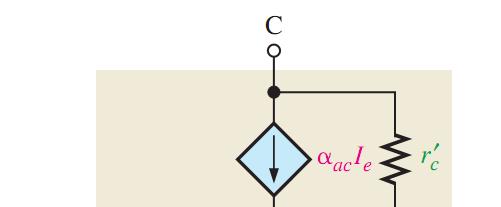
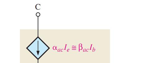
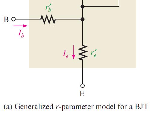
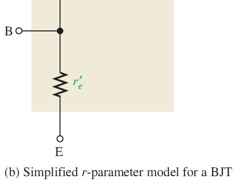
7 Transistor AC Model very large very small 7

8 8

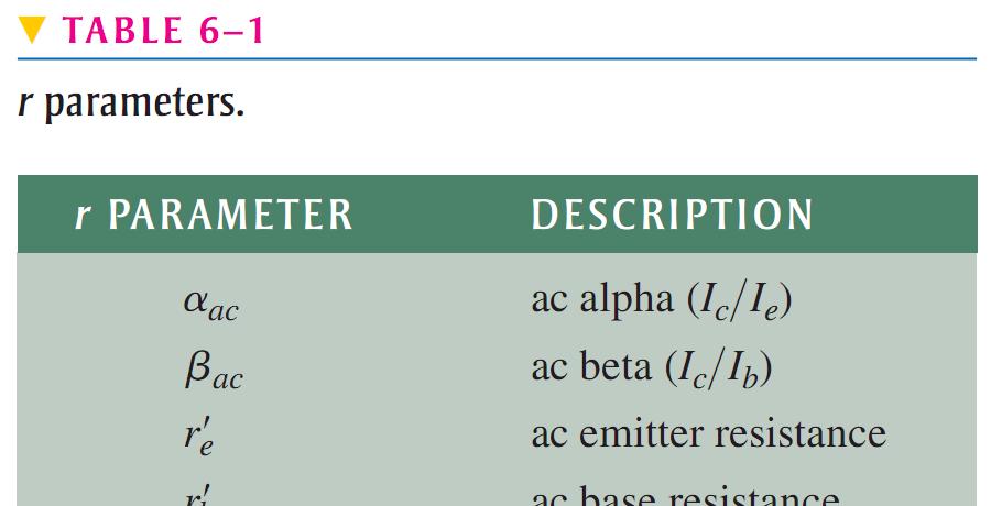
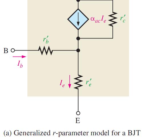
9 Transistor AC Model The five resistance parameters (r-parameters) can be used for detailed analysis of a BJT circuit. For most analysis work, the simplified r-parameters give good results. The simplified r-parameters are shown in relation to the transistor model. An important r-parameter is r e '. It appears as a small ac resistance between the base and emitter. ' r e 25 mv = I assuming an abrupt junction between the n and p regions, and an ambient temperature of 20 C E 9 B C E r e β ac I b B I b C r e E β ac I b
10 Quiz Q. The equation for finding the ac emitter resistance of a BJT is a. b. c. d. ' r e r ' e r ' e r ' e 25 mv = I B E B 25 mv = I E 0.7 V = I 0.7 V = I 10
11 I E = 25 mv / 8 Ω = ma 11

12 Comparison of β ac to β DC Curve of I C versus I B is nonlinear! slope slope 12
")
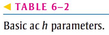

13 h (hybrid) parameters 13
, common-emitter input impedance (resistance), common-emitter")
14 Relationships of h Parameters and r Parameters forward current gain, common-base forward current gain, common-emitter voltage feedback ratio, common-emitter output admittance (conductance), common-emitter input impedance (resistance), common-emitter 14
Electronic Devices. Floyd. Chapter 6. Ninth Edition. Electronic Devices, 9th edition Thomas L. Floyd
 Electronic Devices Ninth Edition Floyd Chapter 6 Agenda BJT AC Analysis Linear Amplifier AC Load Line Transistor AC Model Common Emitter Amplifier Common Collector Amplifier Common Base Amplifier Special
DC Bias. Graphical Analysis. Script
 Course: B.Sc. Applied Physical Science (Computer Science) Year & Sem.: Ist Year, Sem - IInd Subject: Electronics Paper No.: V Paper Title: Analog Circuits Lecture No.: 3 Lecture Title: Analog Circuits
... Second Semester
 كنا نظنك اي عيل تركتنا... لكن طيفك مل يزل يغشانا مثل الندى يسقي النبات بقطره... قد ابت ليال يف ادلىج عطشاان ما زلت أذكر حني أدخل معمال... متسك هجازا للقياس تحاكه... فأ راك جتلس هادئا حيرانا تكتب وترمس
2. SINGLE STAGE BIPOLAR JUNCTION TRANSISTOR (BJT) AMPLIFIERS
 AMPLIFIERS") 2. SINGLE STAGE BIPOLAR JUNCTION TRANSISTOR (BJT) AMPLIFIERS I. Objectives and Contents The goal of this experiment is to become familiar with BJT as an amplifier and to evaluate the basic configurations
2. SINGLE STAGE BIPOLAR JUNCTION TRANSISTOR (BJT) AMPLIFIERS I. Objectives and Contents The goal of this experiment is to become familiar with BJT as an amplifier and to evaluate the basic configurations
By: Dr. Ahmed ElShafee
 Lecture (04) Transistor Bias Circuit 3 BJT Amplifiers 1 By: Dr. Ahmed ElShafee ١ Emitter Feedback Bias If an emitter resistor is added to the base bias circuit in Figure, the result is emitter feedback
5.25Chapter V Problem Set
 5.25Chapter V Problem Set P5.1 Analyze the circuits in Fig. P5.1 and determine the base, collector, and emitter currents of the BJTs as well as the voltages at the base, collector, and emitter terminals.
Electronic Circuits. Power Amplifiers. Manar Mohaisen Office: F208 Department of EECE
 Electronic Circuits Power Amplifiers Manar Mohaisen Office: F208 Email: manar.subhi@kut.ac.kr Department of EECE Review of the Precedent Lecture Explain the Amplifier Operation Explain the BJT AC Models
EE 3111 Lab 7.1. BJT Amplifiers
 EE 3111 Lab 7.1 BJT Amplifiers BJT Amplifier Device/circuit that alters the amplitude of a signal, while keeping input waveform shape BJT amplifiers run the BJT in active mode. Forward current gain is
EXPERIMENT 5 CURRENT AND VOLTAGE CHARACTERISTICS OF BJT
 EXPERIMENT 5 CURRENT AND VOLTAGE CHARACTERISTICS OF BJT 1. OBJECTIVES 1.1 To practice how to test NPN and PNP transistors using multimeter. 1.2 To demonstrate the relationship between collector current
Lecture (01) Transistor operating point & DC Load line
 Transistor operating point & DC Load line") Lecture (01) Transistor operating point & DC Load line By: Dr. Ahmed ElShafee ١ BJT Characteristic Collector Characteristic Curves B C E ٢ BJT modes of operation Conditions in Cutoff Conditions in Saturation
Lecture (01) Transistor operating point & DC Load line By: Dr. Ahmed ElShafee ١ BJT Characteristic Collector Characteristic Curves B C E ٢ BJT modes of operation Conditions in Cutoff Conditions in Saturation
EE105 Fall 2015 Microelectronic Devices and Circuits
 EE105 Fall 2015 Microelectronic Devices and Circuits Prof. Ming C. Wu wu@eecs.berkeley.edu 511 Sutardja Dai Hall (SDH) 11-1 Transistor Operating Mode in Amplifiers Transistors are biased in flat part of
Lecture (04) BJT Amplifiers 1
 BJT Amplifiers 1") Lecture (04) BJT Amplifiers 1 By: Dr. Ahmed ElShafee ١ The Linear Amplifier A linear amplifier provides amplification of a signal without any distortion so that the output signal A voltage divider biased
Lecture (04) BJT Amplifiers 1 By: Dr. Ahmed ElShafee ١ The Linear Amplifier A linear amplifier provides amplification of a signal without any distortion so that the output signal A voltage divider biased
The Bipolar Junction Transistor- Small Signal Characteristics
 The Bipolar Junction Transistor- Small Signal Characteristics Debapratim Ghosh deba21pratim@gmail.com Electronic Systems Group Department of Electrical Engineering Indian Institute of Technology Bombay
SIDDHARTH GROUP OF INSTITUTIONS :: PUTTUR (AUTONOMOUS) Siddharth Nagar, Narayanavanam Road QUESTION BANK
 Siddharth Nagar, Narayanavanam Road QUESTION BANK") SIDDHARTH GROUP OF INSTITUTIONS :: PUTTUR (AUTONOMOUS) Siddharth Nagar, Narayanavanam Road 517583 QUESTION BANK Subject with Code : Electronic Circuit Analysis (16EC407) Year & Sem: II-B.Tech & II-Sem
SIDDHARTH GROUP OF INSTITUTIONS :: PUTTUR (AUTONOMOUS) Siddharth Nagar, Narayanavanam Road 517583 QUESTION BANK Subject with Code : Electronic Circuit Analysis (16EC407) Year & Sem: II-B.Tech & II-Sem
ECE321 Electronics I Fall 2006
 ECE321 Electronics I Fall 2006 Professor James E. Morris Lecture 11 31 st October, 2006 Bipolar Junction Transistors (BJTs) 5.1 Device Structure & Physics 5.2 I-V Characteristics Convert 5.1 information
Homework Assignment 12
 Homework Assignment 12 Question 1 Shown the is Bode plot of the magnitude of the gain transfer function of a constant GBP amplifier. By how much will the amplifier delay a sine wave with the following
BJT Amplifier. Superposition principle (linear amplifier)
") BJT Amplifier Two types analysis DC analysis Applied DC voltage source AC analysis Time varying signal source Superposition principle (linear amplifier) The response of a linear amplifier circuit excited
BJT Amplifier Two types analysis DC analysis Applied DC voltage source AC analysis Time varying signal source Superposition principle (linear amplifier) The response of a linear amplifier circuit excited
BJT AC Analysis CHAPTER OBJECTIVES 5.1 INTRODUCTION 5.2 AMPLIFICATION IN THE AC DOMAIN
 BJT AC Analysis 5 CHAPTER OBJECTIVES Become familiar with the, hybrid, and hybrid p models for the BJT transistor. Learn to use the equivalent model to find the important ac parameters for an amplifier.
EXPERIMENT #3 TRANSISTOR BIASING
 EXPERIMENT #3 TRANSISTOR BIASING Bias (operating point) for a transistor is established by specifying the quiescent (D.C., no signal) values of collector-emitter voltage V CEQ and collector current I CQ.
BJT. Bipolar Junction Transistor BJT BJT 11/6/2018. Dr. Satish Chandra, Assistant Professor, P P N College, Kanpur 1
 BJT Bipolar Junction Transistor Satish Chandra Assistant Professor Department of Physics P P N College, Kanpur www.satish0402.weebly.com The Bipolar Junction Transistor is a semiconductor device which
EE105 Fall 2015 Microelectronic Devices and Circuits. Basic Single-Transistor Amplifier Configurations
 EE05 Fall 205 Microelectronic Devices and Circuits Prof. Ming C. Wu wu@eecs.berkeley.edu 5 Sutardja Dai Hall (SDH 2- MOSFET Basic Single-Transistor Amplifier Configurations BJT 2-2 Two-Port Model of Amplifiers
Microelectronics Circuit Analysis and Design
 Neamen Microelectronics Chapter 6-1 Microelectronics Circuit Analysis and Design Donald A. Neamen Chapter 6 Basic BJT Amplifiers Neamen Microelectronics Chapter 6-2 In this chapter, we will: Understand
Electronic Devices. Floyd. Chapter 7. Ninth Edition. Electronic Devices, 9th edition Thomas L. Floyd
 Electronic Devices Ninth Edition Floyd Chapter 7 Power Amplifiers A power amplifier is a large signal amplifier that produces a replica of the input signal on its output. In the case shown here, the output
Bipolar Junction Transistors
 Bipolar Junction Transistors Invented in 1948 at Bell Telephone laboratories Bipolar junction transistor (BJT) - one of the major three terminal devices Three terminal devices more useful than two terminal
Electronics EECE2412 Spring 2018 Exam #2
 Electronics EECE2412 Spring 2018 Exam #2 Prof. Charles A. DiMarzio Department of Electrical and Computer Engineering Northeastern University 29 March 2018 File:12262/exams/exam2 Name: General Rules: You
LABORATORY MODULE. Analog Electronics. Semester 2 (2005/2006)
") LABORATORY MODULE ENT 162 Analog Electronics Semester 2 (2005/2006) EXPERIMENT 5 : The Class A Common-Emitter Power Amplifier Name Matrix No. : : PUSAT PENGAJIAN KEJURUTERAAN MEKATRONIK KOLEJ UNIVERSITI
LABORATORY MODULE ENT 162 Analog Electronics Semester 2 (2005/2006) EXPERIMENT 5 : The Class A Common-Emitter Power Amplifier Name Matrix No. : : PUSAT PENGAJIAN KEJURUTERAAN MEKATRONIK KOLEJ UNIVERSITI
EXPERIMENT 10: SINGLE-TRANSISTOR AMPLIFIERS 11/11/10
 EXPERIMENT 10: SINGLE-TRANSISTOR AMPLIFIERS 11/11/10 In this experiment we will measure the characteristics of the standard common emitter amplifier. We will use the 2N3904 npn transistor. If you have
Microelectronic Circuits - Fifth Edition Sedra/Smith Copyright 2004 by Oxford University Press, Inc.
 Feedback 1 Figure 8.1 General structure of the feedback amplifier. This is a signal-flow diagram, and the quantities x represent either voltage or current signals. 2 Figure E8.1 3 Figure 8.2 Illustrating
Lab 3: BJT Digital Switch
 Lab 3: BJT Digital Switch Objectives The purpose of this lab is to acquaint you with the basic operation of bipolar junction transistor (BJT) and to demonstrate its functionality in digital switching circuits.
Lecture 8 Power Amplifier (Class A)
") Lecture 8 Power Amplifier (Class A) nduction of Power Amplifier Power and Efficiency Amplifier Classification Basic Class A Amplifier Transformer Coupled Class A Amplifier Ref:08037HKN EE3110 Power Amplifier
Lecture 8 Power Amplifier (Class A) nduction of Power Amplifier Power and Efficiency Amplifier Classification Basic Class A Amplifier Transformer Coupled Class A Amplifier Ref:08037HKN EE3110 Power Amplifier
The shape of the waveform will be the same, but its level is shifted either upward or downward. The values of the resistor R and capacitor C affect
 Diode as Clamper A clamping circuit is used to place either the positive or negative peak of a signal at a desired level. The dc component is simply added or subtracted to/from the input signal. The clamper
So far we have dealt with only small-signal ampliers. In small-signal ampliers the main factors were amplication linearity gain
 Contents Power Amplier Types Class A Operation Class B Operation Class AB Operation Class C Operation Class D Operation Amplier Eciency Series-Fed Class A Amplier AC-DC Load Lines Maximum Eciency Figure
EE 330 Lecture 26. Amplifier Biasing (precursor) Two-Port Amplifier Model
 Two-Port Amplifier Model") EE 330 Lecture 26 Amplifier Biasing (precursor) Two-Port Amplifier Model Exam Schedule Exam 2 Friday October 27 Exam 3 Friday November 17 Review from Last Lecture Graphical Analysis and Interpretation
EE 330 Lecture 26 Amplifier Biasing (precursor) Two-Port Amplifier Model Exam Schedule Exam 2 Friday October 27 Exam 3 Friday November 17 Review from Last Lecture Graphical Analysis and Interpretation
ANALYSIS OF AN NPN COMMON-EMITTER AMPLIFIER
 ANALYSIS OF AN NPN COMMON-EMITTER AMPLIFIER Experiment Performed by: Michael Gonzalez Filip Rege Alexis Rodriguez-Carlson Report Written by: Filip Rege Alexis Rodriguez-Carlson November 28, 2007 Objectives:
Single-Stage BJT Amplifiers and BJT High-Frequency Model. Single-Stage BJT Amplifier Configurations
 1 Single-Stage BJT Amplifiers and BJT High-Frequency Model Asst. Prof. MONTREE SIRIPRUCHYANUN, D. Eng. Dept. of Teacher Training in Electrical Engineering, Faculty of Technical Education King Mongkut s
EXP8: AMPLIFIERS II.
 EXP8: AMPLIFIES II. Objectives. The objectives of this lab are:. To analyze the behavior of a class A amplifier. 2. To understand the role the components play in the gain of the circuit. 3. To find the
Electronic PRINCIPLES
 MALVINO & BATES Electronic PRINCIPLES SEVENTH EDITION Chapter 9 AC Models Topics covered in Chapter 9 Base-biased amplifier Emitter-biased amplifier Small-signal operation AC beta AC resistance of the
Experiment 6: Biasing Circuitry
 1 Objective UNIVERSITY OF CALIFORNIA AT BERKELEY College of Engineering Department of Electrical Engineering and Computer Sciences EE105 Lab Experiments Experiment 6: Biasing Circuitry Setting up a biasing
I C I E =I B = I C 1 V BE 0.7 V
 Guide to NPN Amplifier Analysis Jason Woytowich 1. Transistor characteristics A BJT has three operating modes cutoff, active, and saturation. For applications, like amplifiers, where linear characteristics
Frequency Response of Common Emitter Amplifier
 Başkent University Department of Electrical and Electronics Engineering EEM 311 Electronics II Experiment 6 Frequency Response of Common Emitter Amplifier Aim: The aim of this experiment is to study the
Experiment #6: Biasing an NPN BJT Introduction to CE, CC, and CB Amplifiers
 SCHOOL OF ENGINEERING AND APPLIED SCIENCE DEPARTMENT OF ELECTRICAL AND COMPUTER ENGINEERING ECE 2115: ENGINEERING ELECTRONICS LABORATORY Experiment #6: Biasing an NPN BJT Introduction to CE, CC, and CB
By: Dr. Ahmed ElShafee
 Lecture (02) Transistor operating point & DC Load line (2), Transistor Bias Circuit 1 By: Dr. Ahmed ElShafee ١ DC Load Line The dc operation can be described graphically using a dc load line. This is a
Electronics EECE2412 Spring 2017 Exam #2
 Electronics EECE2412 Spring 2017 Exam #2 Prof. Charles A. DiMarzio Department of Electrical and Computer Engineering Northeastern University 30 March 2017 File:12198/exams/exam2 Name: : General Rules:
Electronic Circuits for Mechatronics ELCT 609 Lecture 5: BJT Voltage Amplifiers
 Electronic Circuits for Mechatronics ELCT 609 Lecture 5: BJT Voltage Amplifiers Assistant Professor Office: C3.315 E-mail: eman.azab@guc.edu.eg 1 BJT Modes of Operation Electrical Equations of BJT 2 BJT
Exam Model Answer. Question 1 (15 marks) Answer this question in the form of table. Choose the correct answer (only one answer is accepted).
 Answer this question in the form of table. Choose the correct answer (only one answer is accepted).") Benha University Faculty of Engineering Shoubra Electrical Engineering Department First Year Communications. Answer all the following questions Illustrate your answers with sketches when necessary. The
Benha University Faculty of Engineering Shoubra Electrical Engineering Department First Year Communications. Answer all the following questions Illustrate your answers with sketches when necessary. The
Experiment #8: Designing and Measuring a Common-Collector Amplifier
 SCHOOL OF ENGINEERING AND APPLIED SCIENCE DEPARTMENT OF ELECTRICAL AND COMPUTER ENGINEERING ECE 2115: ENGINEERING ELECTRONICS LABORATORY Experiment #8: Designing and Measuring a Common-Collector Amplifier
Federal Urdu University of Arts, Science & Technology Islamabad Pakistan THIRD SEMESTER ELECTRONICS - II BASIC ELECTRICAL & ELECTRONICS LAB
 THIRD SEMESTER ELECTRONICS - II BASIC ELECTRICAL & ELECTRONICS LAB DEPARTMENT OF ELECTRICAL ENGINEERING Prepared By: Checked By: Approved By: Engr. Saqib Riaz Engr. M.Nasim Khan Dr.Noman Jafri Lecturer
Module-1 BJT AC Analysis: The re Transistor Model. Common-Base Configuration
 Module-1 BJT AC Analysis: BJT AC Analysis: BJT AC Analysis: BJT Transistor Modeling, The re transistor model, Common emitter fixed bias, Voltage divider bias, Emitter follower configuration. Darlington
Experiment 6: Biasing Circuitry
 1 Objective UNIVERSITY OF CALIFORNIA AT BERKELEY College of Engineering Department of Electrical Engineering and Computer Sciences EE105 Lab Experiments Experiment 6: Biasing Circuitry Setting up a biasing
Current Mirrors. Basic BJT Current Mirror. Current mirrors are basic building blocks of analog design. Figure shows the basic NPN current mirror.
 Current Mirrors Basic BJT Current Mirror Current mirrors are basic building blocks of analog design. Figure shows the basic NPN current mirror. For its analysis, we assume identical transistors and neglect
Electron Devices and Circuits
 Electron Devices and Circuits (EC 8353) Prepared by Mr.R.Suresh, AP/EEE Ms.S.KARKUZHALI,A.P/EEE BJT small signal model Analysis of CE, CB, CC amplifiers- Gain and frequency response MOSFET small signal
CHAPTER 3: BIPOLAR JUNCION TRANSISTOR DR. PHẠM NGUYỄN THANH LOAN
 CHAPTER 3: BIPOLAR JUNCION TRANSISTOR DR. PHẠM NGUYỄN THANH LOAN Hanoi, 9/24/2012 Contents 2 Structure and operation of BJT Different configurations of BJT Characteristic curves DC biasing method and analysis
R a) Draw and explain VI characteristics of Si & Ge diode. (8M) b) Explain the operation of SCR & its characteristics (8M)
 Draw and explain VI characteristics of Si & Ge diode. (8M) b) Explain the operation of SCR & its characteristics (8M)") SET - 1 1. a) Define i) transient capacitance ii) Diffusion capacitance (4M) b) Explain Fermi level in intrinsic and extrinsic semiconductor (4M) c) Derive the expression for ripple factor of Half wave
SET - 1 1. a) Define i) transient capacitance ii) Diffusion capacitance (4M) b) Explain Fermi level in intrinsic and extrinsic semiconductor (4M) c) Derive the expression for ripple factor of Half wave
Carleton University ELEC Lab 1. L2 Friday 2:30 P.M. Student Number: Operation of a BJT. Author: Adam Heffernan
 Carleton University ELEC 3509 Lab 1 L2 Friday 2:30 P.M. Student Number: 100977570 Operation of a BJT Author: Adam Heffernan October 13, 2017 Contents 1 Transistor DC Characterization 3 1.1 Calculations
UNIVERSITY OF PENNSYLVANIA EE 206
 UNIVERSITY OF PENNSYLVANIA EE 206 TRANSISTOR BIASING CIRCUITS Introduction: One of the most critical considerations in the design of transistor amplifier stages is the ability of the circuit to maintain
Tutorial 2 BJTs, Transistor Bias Circuits, BJT Amplifiers FETs and FETs Amplifiers. Part 1: BJTs, Transistor Bias Circuits and BJT Amplifiers
 Tutorial 2 BJTs, Transistor Bias Circuits, BJT Amplifiers FETs and FETs Amplifiers Part 1: BJTs, Transistor Bias Circuits and BJT Amplifiers 1. Explain the purpose of a thin, lightly doped base region.
EEE225: Analogue and Digital Electronics
 EEE225: Analogue and Digital Electronics Lecture II James E. Green Department of Electronic Engineering University of Sheffield j.e.green@sheffield.ac.uk This Lecture 1 One Transistor Circuits Continued...
Lecture 18: Common Emitter Amplifier.
 Whites, EE 320 Lecture 18 Page 1 of 8 Lecture 18: Common Emitter Amplifier. We will now begin the analysis of the three basic types of linear BJT small-signal amplifiers: 1. Common emitter (CE) 2. Common
Chapter 3: Bipolar Junction Transistors
 Chapter 3: Bipolar Junction Transistors Transistor Construction There are two types of transistors: pnp npn pnp The terminals are labeled: E - Emitter B - Base C - Collector npn 2 Transistor Operation
BIPOLAR JUNCTION TRANSISTORS (BJTs) Dr Derek Molloy, DCU
 Dr Derek Molloy, DCU") IPOLAR JUNCTION TRANSISTORS (JTs) Dr Derek Molloy, DCU What are JTs? Two PN junctions joined together is a JT Simply known as a transistor! ipolar? Current carried by electrons and holes Will see FETs
IPOLAR JUNCTION TRANSISTORS (JTs) Dr Derek Molloy, DCU What are JTs? Two PN junctions joined together is a JT Simply known as a transistor! ipolar? Current carried by electrons and holes Will see FETs
Transistor Biasing. DC Biasing of BJT. Transistor Biasing. Transistor Biasing 11/23/2018
 Transistor Biasing DC Biasing of BJT Satish Chandra Assistant Professor Department of Physics P P N College, Kanpur www.satish0402.weebly.com A transistors steady state of operation depends a great deal
BJT Characteristics & Common Emitter Transistor Amplifier
 LAB #07 Objectives 1. To graph the collector characteristics of a transistor. 2. To measure AC and DC voltages in a common-emitter amplifier. Theory BJT A bipolar (junction) transistor (BJT) is a three-terminal
Experiment No. 9 DESIGN AND CHARACTERISTICS OF COMMON BASE AND COMMON COLLECTOR AMPLIFIERS
 Experiment No. 9 DESIGN AND CHARACTERISTICS OF COMMON BASE AND COMMON COLLECTOR AMPLIFIERS 1. Objective: The objective of this experiment is to explore the basic applications of the bipolar junction transistor
Crystal Oscillator. Circuit symbol
 Crystal Oscillator Crystal Oscillator Piezoelectric crystal (quartz) Operates as a resonant circuit Shows great stability in oscillation frequency Piezoelectric effect : When mechanical stress is applied
Başkent University Department of Electrical and Electronics Engineering EEM 214 Electronics I Experiment 8. Bipolar Junction Transistor
 Başkent University Department of Electrical and Electronics Engineering EEM 214 Electronics I Experiment 8 Bipolar Junction Transistor Aim: The aim of this experiment is to investigate the DC behavior
Expanded Answer: Transistor Amplifier Problem in January/February 2008 Morseman Column
 Expanded Answer: Transistor Amplifier Problem in January/February 2008 Morseman Column Here s what I asked: This month s problem: Figure 4(a) shows a simple npn transistor amplifier. The transistor has
Linear electronic. Lecture No. 1
 1 Lecture No. 1 2 3 4 5 Lecture No. 2 6 7 8 9 10 11 Lecture No. 3 12 13 14 Lecture No. 4 Example: find Frequency response analysis for the circuit shown in figure below. Where R S =4kR B1 =8kR B2 =4k R
Electronic Circuits EE359A
 Electronic Circuits EE359A Bruce McNair B206 bmcnair@stevens.edu 201-216-5549 Lecture 4 0 Bipolar Junction Transistors (BJT) Small Signal Analysis Graphical Analysis / Biasing Amplifier, Switch and Logic
Lab 2: Common Emitter Design: Part 2
 Lab 2: Common Emitter Design: Part 2 ELE 344 University of Rhode Island, Kingston, RI 02881-0805, U.S.A. 1 Linearity in High Gain Amplifiers The common emitter amplifier, shown in figure 1, will provide
EEE225: Analogue and Digital Electronics
 EEE225: Analogue and Digital Electronics Lecture I James E. Green Department of Electronic Engineering University of Sheffield j.e.green@sheffield.ac.uk Introduction This Lecture 1 Introduction Aims &
 Code No: Y0221/R07 Set No. 1 I B.Tech Supplementary Examinations, Apr/May 2013 BASIC ELECTRONIC DEVICES AND CIRCUITS (Electrical & Electronics Engineering) Time: 3 hours Max Marks: 80 Answer any FIVE Questions
Electronic Troubleshooting. Chapter 5 Multistage Amplifiers
 Electronic Troubleshooting Chapter 5 Multistage Amplifiers Overview When more amplification is required than can be supplied by a single stage amp A second stage is added Or more stages are added Aspects
Physics 623 Transistor Characteristics and Single Transistor Amplifier Sept. 12, 2017
 Physics 623 Transistor Characteristics and Single Transistor Amplifier Sept. 12, 2017 1 Purpose To measure and understand the common emitter transistor characteristic curves. To use the base current gain
Lecture #3 ( 2 weeks) Transistors
 Transistors") Spring 2015 Benha University Faculty of Engineering at Shoubra ECE-291 Electronic Engineering Lecture #3 ( 2 weeks) Transistors Instructor: Dr. Ahmad El-Banna 1 Agenda BJT Structure Basic Operation Transistor
Spring 2015 Benha University Faculty of Engineering at Shoubra ECE-291 Electronic Engineering Lecture #3 ( 2 weeks) Transistors Instructor: Dr. Ahmad El-Banna 1 Agenda BJT Structure Basic Operation Transistor
Chapter Three " BJT Small-Signal Analysis "
 Chapter Three " BJT Small-Signal Analysis " We now begin to examine the small-signal ac response of the BJT amplifier by reviewing the models most frequently used to represent the transistor in the sinusoidal
Small signal ac equivalent circuit of BJT
 UNIT-2 Part A 1. What is an ac load line? [N/D 16] A dc load line gives the relationship between the q-point and the transistor characteristics. When capacitors are included in a CE transistor circuit,
ECE 255, Discrete-Circuit Amplifiers
 ECE 255, Discrete-Circuit Amplifiers 20 March 2018 In this lecture, we will continue with the study of transistor amplifiers with the presence of biasing circuits and coupling capacitors in place. We will
SAMPLE FINAL EXAMINATION FALL TERM
 ENGINEERING SCIENCES 154 ELECTRONIC DEVICES AND CIRCUITS SAMPLE FINAL EXAMINATION FALL TERM 2001-2002 NAME Some Possible Solutions a. Please answer all of the questions in the spaces provided. If you need
Understanding VCO Concepts
 Understanding VCO Concepts OSCILLATOR FUNDAMENTALS An oscillator circuit can be modeled as shown in Figure 1 as the combination of an amplifier with gain A (jω) and a feedback network β (jω), having frequency-dependent
(a) BJT-OPERATING MODES & CONFIGURATIONS
 BJT-OPERATING MODES & CONFIGURATIONS") (a) BJT-OPERATING MODES & CONFIGURATIONS 1. The leakage current I CBO flows in (a) The emitter, base and collector leads (b) The emitter and base leads. (c) The emitter and collector leads. (d) The base
(a) BJT-OPERATING MODES & CONFIGURATIONS 1. The leakage current I CBO flows in (a) The emitter, base and collector leads (b) The emitter and base leads. (c) The emitter and collector leads. (d) The base
Chapter 12 Power Amplifier
 Chapter 12 Power Amplifier Definitions In small-signal amplifiers the main factors are: Amplification Linearity Gain Since large-signal, or power, amplifiers handle relatively large voltage signals and
Transistor Configuration
 Transistor Configuration 1 Objectives To review BJT biasing circuit. To study BJT amplifier circuit To understand the BJT configuration. To analyse single-stage BJT amplifier circuits. To study the differential
Electronic Circuits ELCT604 (Spring 2018) Lecture 2 BJT Amplifiers
 Lecture 2 BJT Amplifiers") Electronic Circuits ELCT604 (Spring 2018) Lecture 2 BJT Amplifiers Assistant Professor Office: C3.315 E-mail: eman.azab@guc.edu.eg 1 Analog Voltage Amplifiers Circuit Design and Configurations 2 Objective
Electronic Circuits ELCT604 (Spring 2018) Lecture 2 BJT Amplifiers Assistant Professor Office: C3.315 E-mail: eman.azab@guc.edu.eg 1 Analog Voltage Amplifiers Circuit Design and Configurations 2 Objective
Electronic Circuits - Tutorial 07 BJT transistor 1
 Electronic Circuits - Tutorial 07 BJT transistor 1-1 / 20 - T & F # Question 1 A bipolar junction transistor has three terminals. T 2 For operation in the linear or active region, the base-emitter junction
Lab 2: Discrete BJT Op-Amps (Part I)
") Lab 2: Discrete BJT Op-Amps (Part I) This is a three-week laboratory. You are required to write only one lab report for all parts of this experiment. 1.0. INTRODUCTION In this lab, we will introduce and
Lab 2: Discrete BJT Op-Amps (Part I) This is a three-week laboratory. You are required to write only one lab report for all parts of this experiment. 1.0. INTRODUCTION In this lab, we will introduce and
Physics 116A Fall 2000: Final Exam
 Physics 6A Fall 2000: Final Exam 2//2000 (rev. 2/0) Closed book and notes except for three 8.5 in 2 sheets of paper. Show reasoning for full credit. There are 6 problems and 200 points. Note: complex quantities
Component modeling. Resources and methods for learning about these subjects (list a few here, in preparation for your research):
:") Component modeling This worksheet and all related files are licensed under the Creative Commons Attribution License, version 1.0. To view a copy of this license, visit http://creativecommons.org/licenses/by/1.0/,
Component modeling This worksheet and all related files are licensed under the Creative Commons Attribution License, version 1.0. To view a copy of this license, visit http://creativecommons.org/licenses/by/1.0/,
EC1203: ELECTRONICS CIRCUITS-I UNIT-I TRANSISTOR BIASING PART-A
 SHRI ANGALAMMAN COLLEGE OF ENGG & TECH., TRICHY 621105 (Approved by AICTE, New Delhi and Affiliated to Anna University Chennai/Trichy) ( ISO 9001:2008 Certified Institution) DEPARTMENT OF ELECTRONICS &
Lecture #4 BJT AC Analysis
 November 2014 Ahmad El-Banna Integrated Technical Education Cluster At AlAmeeria J-601-1448 Electronic Principals Lecture #4 BJT AC Analysis Instructor: Dr. Ahmad El-Banna Agenda BJT transistor Modeling
Chapter 3. Bipolar Junction Transistors
 Chapter 3. Bipolar Junction Transistors Outline: Fundamental of Transistor Common-Base Configuration Common-Emitter Configuration Common-Collector Configuration Introduction The transistor is a three-layer
Transistor Configuration
 Transistor Configuration 1 Objectives To review BJT biasing circuit. To study BJT amplifier circuit To understand the BJT configuration. To analyse single-stage BJT amplifier circuits. To study the differential
Transistor Biasing and Operational amplifier fundamentals. OP-amp Fundamentals and its DC characteristics. BJT biasing schemes
 Lab 1 Transistor Biasing and Operational amplifier fundamentals Experiment 1.1 Experiment 1.2 BJT biasing OP-amp Fundamentals and its DC characteristics BJT biasing schemes 1.1 Objective 1. To sketch potential
HOME ASSIGNMENT. Figure.Q3
 HOME ASSIGNMENT 1. For the differential amplifier circuit shown below in figure.q1, let I=1 ma, V CC =5V, v CM = -2V, R C =3kΩ and β=100. Assume that the BJTs have v BE =0.7 V at i C =1 ma. Find the voltage
Experiment 8 Frequency Response
 Experiment 8 Frequency Response W.T. Yeung, R.A. Cortina, and R.T. Howe UC Berkeley EE 105 Spring 2005 1.0 Objective This lab will introduce the student to frequency response of circuits. The student will
UNIT I BIASING OF DISCRETE BJT AND MOSFET PART A
 UNIT I BIASING OF DISCRETE BJT AND MOSFET PART A 1. Why do we choose Q point at the center of the load line? 2. Name the two techniques used in the stability of the q point.explain. 3. Give the expression
ANALOG FUNDAMENTALS C. Topic 4 BASIC FET AMPLIFIER CONFIGURATIONS
 AV18-AFC ANALOG FUNDAMENTALS C Topic 4 BASIC FET AMPLIFIER CONFIGURATIONS 1 ANALOG FUNDAMENTALS C AV18-AFC Overview This topic identifies the basic FET amplifier configurations and their principles of
STATIC CHARACTERISTICS OF TRANSISTOR
 STAT CHARACTERISTS OF TRANSISTOR OBJECTIVE The purpose of the experiment is to study the characteristics of bipolar transistor in common emitter (CE) configuration. From the characteristic curve it is
UNIVERSITY OF NORTH CAROLINA AT CHARLOTTE Department of Electrical and Computer Engineering
 UNIVERSITY OF NORTH CAROLINA AT CHARLOTTE Department of Electrical and Computer Engineering EXPERIMENT 7 BJT AMPLIFIER CONFIGURATIONS AND INPUT/OUTPUT IMPEDANCE OBJECTIVES The purpose of this experiment
V o2 = V c V d 2. V o1. Sensor circuit. Figure 1: Example of common-mode and difference-mode voltages. V i1 Sensor circuit V o
 M.B. Patil, IIT Bombay 1 BJT Differential Amplifier Common-mode and difference-mode voltages A typical sensor circuit produces an output voltage between nodes A and B (see Fig. 1) such that V o1 = V c
Bipolar junction transistors.
 Bipolar junction transistors. Third Semester Course code : 15EECC202 Analog electronic circuits (AEC) Team: Dr. Nalini C Iyer, R.V. Hangal, Sujata N, Prashant A, Sneha Meti AEC Team, Faculty, School of