By: Dr. Ahmed ElShafee
|
|
|
- Mariah Morrison
- 5 years ago
- Views:
Transcription


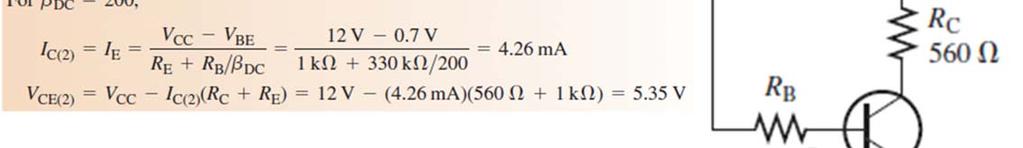
1 Lecture (04) Transistor Bias Circuit 3 BJT Amplifiers 1 By: Dr. Ahmed ElShafee ١ Emitter Feedback Bias If an emitter resistor is added to the base bias circuit in Figure, the result is emitter feedback bias. If the collector current tries to increase, the emitter voltage increases, causing an increase in base voltage because VB =VE + VBE. This increase in base voltage reduces the voltage across RB, thus reducing the base current and keeping the collector current from increasing. ٢
2 A similar action occurs if the collector current tries to decrease. While this is better for linear circuits than base bias, it is still dependent on βdc and is not as predictable as voltage divider bias. ٣ Kirchhoff s voltage law KVL I E = I c = V CC I C R C V CE I E R E = 0 V CE =V CC I C R C R E I C ٤


3 Example 04 ٥ ٦

4 ٧ Collector Feedback Bias The collector voltage provides the bias for the base emitter junction. The negative feedback creates an offsetting effect that tends to keep the Q point stable. When VC decreases, there is a decrease in voltage across RB, which decreases IB. The decrease in IB produces less IC which, in turn, drops less voltage across RC and thus offsets the increase in VC. ٨

5 ٩ Ohm s law Let s assume that I C >>I B The collector voltage is Substituting The terms can be arranged ١٠
6 solve for IC Since the emitter is ground, VCE = VC ١١ Q Point Stability Over Temperature Equation shows that the collector current is dependent to some extent on β, V BE This dependency, increase if R C >>R B /β, V CC >>V BE β varies directly with temperature, V BE varies inversely with temperature. As the temperature goes up in a collectorfeedback circuit, β goes up and VBE goes down ١٢
7 The increase in β acts to increase IC. The decrease in VBE acts to increase IB which, in turn also acts to increase IC. As IC tries to increase, the voltage drop across RC also tries to increase. This tends to reduce the collector voltage and therefore the voltage across RB, reducing IB and offsetting the attempted increase in IC and the attempted decrease in VC. ١٣ ١٤


8 Example 05 Calculate the Q point values (IC and VCE) for the circuit in Figure ١٥ ١٦

9 summery Emitter Bias Emitter Bias Base Bias Emitter Feedback Bias
10 Collector Feedback Bias The Linear Amplifier A linear amplifier provides amplification of a signal without any distortion so that the output signal A voltage divider biased transistor with a sinusoidal ac source capacitively coupled to the base through C1 and a load capacitively coupled to the collector through C2 is shown in Figure ٢٠
11 The collector current varies above and below its Q point value, ICQ, in phase with the base current. The sinusoidal collector to emitter voltage varies above and below its Q point value, VCEQ, 180 out of phase with the base voltage ٢١ The operation just described can be illustrated graphically on the ac load line, as shown sinusoidal voltage at the base produces a base current that varies above and below the Q point on the ac load line The ac load line differs from the dc load line because the effective ac collector resistance is RL in parallel with RC and is less than the dc collector resistance RC alone. ٢٢


12 Example 01 ٢٣ collector current varying from 6 ma to 4 ma for a peak topeak value of 2 ma and the collector to emitter voltage varying from 1 V to 2 V for a peak to peak value of 1 V. ٢٤

; several hundred")


13 TRANSISTOR AC MODELS The five r parameters commonly used for BJTs are (r b); small enough to neglect (r c); several hundred kilohms and can be replaced by an open. The collector effectively acts as a dependent current source of or, equivalently, ٢٥ ٢٦


14 ٢٧ assuming an abrupt junction between the n and p regions. It is also temperature dependent and is based on an ambient temperature of 20 C. ٢٨

15 Example 02 ٢٩ ٣٠
16 Comparison of the AC Beta ( βac) to the DC Beta (βdc) For a typical transistor, a graph of IC versus IB is nonlinear, as shown in Figure. If you pick a Q point on the curve and cause the base current to vary an amount Δ IB then the collector current will vary an Δ IC amount as shown in part (b). ٣١ At different points on the nonlinear curve, the ratio Δ IC / ΔIB will be different, and it may also differ from the IC /IBratio at the Q point. ٣٢

 parameters (hi,")


17 h Parameters A manufacturer s datasheet typically specifies h (hybrid) parameters (hi, hr, hf, and ho) Basic ac h parameters. ٣٣ Subscripts of h parameters for each of the three amplifier configurations ٣٤
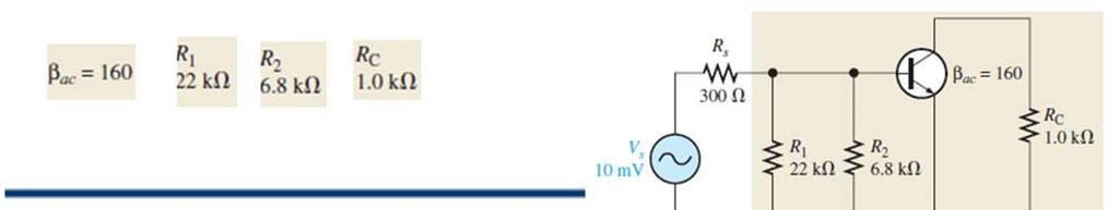
18 Relationships of h Parameters and r Parameters datasheets often provide only common emitter h parameters, the following formulas show how to convert them to r parameters. ٣٥ THE COMMON EMITTER AMPLIFIER common emitter amplifier with voltage divider bias and coupling capacitors C1 and C3 on the input and output and a bypass capacitor, C2, from emitter to ground. ٣٦
19 There is no signal at the emitter because the bypass capacitor effectively shorts the emitter to ground at the signal frequency. All amplifiers have a combination of both ac and dc operation, which must be considered, but keep in mind that the common emitter designation refers to the ac operation. ٣٧ Phase Inversion The output signal is 180 out of phase with the input signal. As the input signal voltage changes, it causes the ac base current to change, resulting in a change in the collector current from its Q point value. If the base current increases, the collector current increases above its Q point value, causing an increase in the voltage drop across RC. This increase in the voltage across RC means that the voltage at the collector decreases from its Q point. So, any change in input signal voltage results in an opposite change in collector signal voltage, which is a phase inversion. ٣٨


20 DC Analysis a dc equivalent circuit is developed by removing the coupling and bypass capacitors ٣٩ circuit can be redrawn Calculate V TH, R TH ٤٠

21 ٤١ AC Analysis The capacitors C1, C2, and C3 are replaced by effective shorts because their values are selected so that XC is negligible at the signal frequency and can be considered to be 0 ohm The dc source is replaced by ground ٤٢

22 is called a common emitter amplifier because the bypass capacitor C2 keeps the emitter at ac ground ٤٣ If the internal resistance of the ac source is then all of the source voltage appears at the base terminal. If, however, the ac source has a nonzero internal resistance, then three factors must be taken into account in determining the actual signal voltage at the base. ٤٤

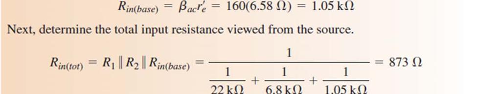
23 R1, R2, and Rin(base) in parallel to get the total input resistance, Rin(tot), A high value of input resistance is desirable so that the amplifier will not excessively load the signal source. This is opposite to the requirement for a stable Q point, which requires smaller resistors. many trade offs that must be considered when choosing components for a circuit. ٤٥ ٤٦

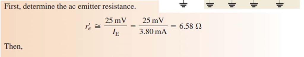
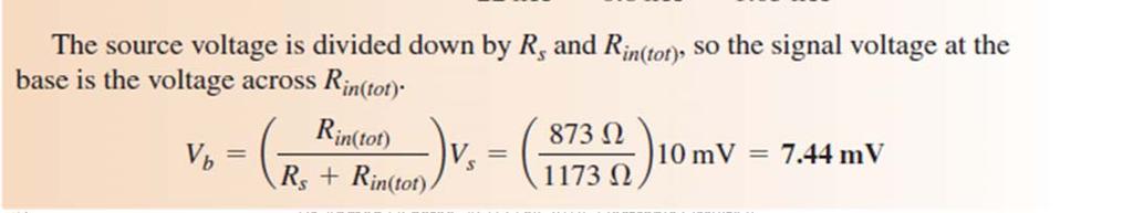
24 Vs, is divided down by Rs (source resistance) and Rin(tot) so ٤٧ use the simplified r parameter model of the transistor. Figure shows the transistor model connected to the external collector resistor, RC ٤٨
25 ٤٩ The output resistance of the commonemitter amplifier is the resistance looking in at the collector since the internal ac collector resistance of the transistor, is typically much larger than RC, the approximation is usually valid ٥٠

26 Example 03 ٥١ ٥٢

27 Voltage Gain The gain is the ratio of ac output voltage at the collector (Vc) to ac input voltage at the base (Vb). ٥٣ Attenuation is the reduction in signal voltage as it passes through a circuit and corresponds to a gain of less than 1. if the signal amplitude is reduced by half, the attenuation is 2, which can be expressed as a gain of 0.5. Suppose a source produces a 10 mv input signal and the source resistance combined with the load resistance results in a 2 mv output signal. In this case, the attenuation is 10 mv/2 mv = 5 gain as 1 /5 =0.2. ٥٤
28 The overall voltage gain of the amplifier ٥٥ Thanks,.. See you next week (ISA), ٥٦
Lecture (04) BJT Amplifiers 1
 BJT Amplifiers 1") Lecture (04) BJT Amplifiers 1 By: Dr. Ahmed ElShafee ١ The Linear Amplifier A linear amplifier provides amplification of a signal without any distortion so that the output signal A voltage divider biased
Lecture (04) BJT Amplifiers 1 By: Dr. Ahmed ElShafee ١ The Linear Amplifier A linear amplifier provides amplification of a signal without any distortion so that the output signal A voltage divider biased
Chapter 5 Transistor Bias Circuits
 Chapter 5 Transistor Bias Circuits Objectives Discuss the concept of dc biasing of a transistor for linear operation Analyze voltage-divider bias, base bias, and collector-feedback bias circuits. Basic
Lecture (06) BJT Amplifiers 3
 BJT Amplifiers 3") Lecture (06) BJT Amplifiers 3 By: Dr. Ahmed ElShafee 1 Current Gain 2 Power Gain The overall power gain is the product of the overall voltage gain (Av ) and the overall current gain (Ai). 3 THE COMMON
Lecture (06) BJT Amplifiers 3 By: Dr. Ahmed ElShafee 1 Current Gain 2 Power Gain The overall power gain is the product of the overall voltage gain (Av ) and the overall current gain (Ai). 3 THE COMMON
Electrical, Electronic and Digital Principles (EEDP) Lecture 3. Other BJT Biasing Techniques باسم ممدوح الحلوانى
 Lecture 3. Other BJT Biasing Techniques باسم ممدوح الحلوانى") Electrical, Electronic and Digital Principles (EEDP) Lecture 3 Other BJT Biasing Techniques د. باسم ممدوح الحلوانى Approximate Analysis Voltage-divider Bias Exact Analysis Ri = is the equivalent resistance
Electrical, Electronic and Digital Principles (EEDP) Lecture 3 Other BJT Biasing Techniques د. باسم ممدوح الحلوانى Approximate Analysis Voltage-divider Bias Exact Analysis Ri = is the equivalent resistance
Lab 4. Transistor as an amplifier, part 2
 Lab 4 Transistor as an amplifier, part 2 INTRODUCTION We continue the bi-polar transistor experiments begun in the preceding experiment. In the common emitter amplifier experiment, you will learn techniques
Lecture (05) BJT Amplifiers 2
 BJT Amplifiers 2") Lecture (05) BJT Amplifiers 2 By: Dr. Ahmed ElShafee 1 Effect of the Emitter Bypass Capacitor on Voltage Gain The emitter bypass capacitor, provides an effective short to the ac signal around the emitter
Lecture (05) BJT Amplifiers 2 By: Dr. Ahmed ElShafee 1 Effect of the Emitter Bypass Capacitor on Voltage Gain The emitter bypass capacitor, provides an effective short to the ac signal around the emitter
DEPARTMENT OF ELECTRONICS AND COMMUNICATION ENGINEERING III SEMESTER EC 6304 ELECTRONIC CIRCUITS I. (Regulations 2013)
") DEPARTMENT OF ELECTRONICS AND COMMUNICATION ENGINEERING III SEMESTER EC 6304 ELECTRONIC CIRCUITS I (Regulations 2013 UNIT-1 Part A 1. What is a Q-point? [N/D 16] The operating point also known as quiescent
DEPARTMENT OF ELECTRONICS AND COMMUNICATION ENGINEERING III SEMESTER EC 6304 ELECTRONIC CIRCUITS I (Regulations 2013 UNIT-1 Part A 1. What is a Q-point? [N/D 16] The operating point also known as quiescent
The George Washington University School of Engineering and Applied Science Department of Electrical and Computer Engineering ECE 20 - LAB
 The George Washington University School of Engineering and Applied Science Department of Electrical and Computer Engineering ECE 20 - LAB Experiment # 6 (Part I) Bipolar Junction Transistors Common Emitter
REVIEW TRANSISTOR BIAS CIRCUIT
 EVIEW TANSISTO BIAS CICUIT OBJECTIVES Discuss the concept of dc biasing of a transistor for linear operation Analyze voltage-divider bias, base bias, and collectorfeedback bias circuits. Basic troubleshooting
Chapter 6. BJT Amplifiers
 Basic Electronic Devices and Circuits EE 111 Electrical Engineering Majmaah University 2 nd Semester 1432/1433 H Chapter 6 BJT Amplifiers 1 Introduction The things you learned about biasing a transistor
Lecture (06) BJT Amplifiers 3
 BJT Amplifiers 3") Lecture (06) BJT Amplifiers 3 By: Dr. Ahmed ElShafee ١ THE COMMON COLLECTOR AMPLIFIER An emitter follower circuit with voltage divider bias is shown in Figure, the input signal is capacitively coupled
Lecture (06) BJT Amplifiers 3 By: Dr. Ahmed ElShafee ١ THE COMMON COLLECTOR AMPLIFIER An emitter follower circuit with voltage divider bias is shown in Figure, the input signal is capacitively coupled
By: Dr. Ahmed ElShafee
 Lecture (02) Transistor operating point & DC Load line (2), Transistor Bias Circuit 1 By: Dr. Ahmed ElShafee ١ DC Load Line The dc operation can be described graphically using a dc load line. This is a
Lecture (09) Bipolar Junction Transistor 3
 Bipolar Junction Transistor 3") Lecture (09) Bipolar Junction Transistor 3 By: Dr. Ahmed ElShafee ١ I THE BJT AS AN AMPLIFIER Amplification is the process of linearly increasing the amplitude of an electrical signal and is one of the
Lecture (09) Bipolar Junction Transistor 3 By: Dr. Ahmed ElShafee ١ I THE BJT AS AN AMPLIFIER Amplification is the process of linearly increasing the amplitude of an electrical signal and is one of the
Chapter Two "Bipolar Transistor Circuits"
 Chapter Two "Bipolar Transistor Circuits" 1.TRANSISTOR CONSTRUCTION:- The transistor is a three-layer semiconductor device consisting of either two n- and one p-type layers of material or two p- and one
ET215 Devices I Unit 4A
 ITT Technical Institute ET215 Devices I Unit 4A Chapter 3, Section 3.1-3.2 This unit is divided into two parts; Unit 4A and Unit 4B Chapter 3 Section 3.1 Structure of Bipolar Junction Transistors The basic
E84 Lab 3: Transistor
 E84 Lab 3: Transistor Cherie Ho and Siyi Hu April 18, 2016 Transistor Testing 1. Take screenshots of both the input and output characteristic plots observed on the semiconductor curve tracer with the following
Lecture (01) Transistor operating point & DC Load line
 Transistor operating point & DC Load line") Lecture (01) Transistor operating point & DC Load line By: Dr. Ahmed ElShafee ١ BJT Characteristic Collector Characteristic Curves B C E ٢ BJT modes of operation Conditions in Cutoff Conditions in Saturation
Lecture (01) Transistor operating point & DC Load line By: Dr. Ahmed ElShafee ١ BJT Characteristic Collector Characteristic Curves B C E ٢ BJT modes of operation Conditions in Cutoff Conditions in Saturation
Bipolar Junction Transistors
 Bipolar Junction Transistors Invented in 1948 at Bell Telephone laboratories Bipolar junction transistor (BJT) - one of the major three terminal devices Three terminal devices more useful than two terminal
Lecture (07) BJT Amplifiers 4 JFET (1)
 BJT Amplifiers 4 JFET (1)") Lecture (07) BJT Amplifiers 4 JFET (1) By: r. Ahmed Elhafee 1 Capacitively Coupled Multistage Amplifier we will use the two stage capacitively coupled amplifier in Figure The output of the first stage
Lecture (07) BJT Amplifiers 4 JFET (1) By: r. Ahmed Elhafee 1 Capacitively Coupled Multistage Amplifier we will use the two stage capacitively coupled amplifier in Figure The output of the first stage
2. SINGLE STAGE BIPOLAR JUNCTION TRANSISTOR (BJT) AMPLIFIERS
 AMPLIFIERS") 2. SINGLE STAGE BIPOLAR JUNCTION TRANSISTOR (BJT) AMPLIFIERS I. Objectives and Contents The goal of this experiment is to become familiar with BJT as an amplifier and to evaluate the basic configurations
2. SINGLE STAGE BIPOLAR JUNCTION TRANSISTOR (BJT) AMPLIFIERS I. Objectives and Contents The goal of this experiment is to become familiar with BJT as an amplifier and to evaluate the basic configurations
I C I E =I B = I C 1 V BE 0.7 V
 Guide to NPN Amplifier Analysis Jason Woytowich 1. Transistor characteristics A BJT has three operating modes cutoff, active, and saturation. For applications, like amplifiers, where linear characteristics
Module-1 BJT AC Analysis: The re Transistor Model. Common-Base Configuration
 Module-1 BJT AC Analysis: BJT AC Analysis: BJT AC Analysis: BJT Transistor Modeling, The re transistor model, Common emitter fixed bias, Voltage divider bias, Emitter follower configuration. Darlington
DC Bias. Graphical Analysis. Script
 Course: B.Sc. Applied Physical Science (Computer Science) Year & Sem.: Ist Year, Sem - IInd Subject: Electronics Paper No.: V Paper Title: Analog Circuits Lecture No.: 3 Lecture Title: Analog Circuits
Analog Circuits Prof. Jayanta Mukherjee Department of Electrical Engineering Indian Institute of Technology - Bombay
 Analog Circuits Prof. Jayanta Mukherjee Department of Electrical Engineering Indian Institute of Technology - Bombay Week - 08 Module - 04 BJT DC Circuits Hello, welcome to another module of this course
Emitter base bias. Collector base bias Active Forward Reverse Saturation forward Forward Cut off Reverse Reverse Inverse Reverse Forward
 SEMICONDUCTOR PHYSICS-2 [Transistor, constructional characteristics, biasing of transistors, transistor configuration, transistor as an amplifier, transistor as a switch, transistor as an oscillator] Transistor
Figure1: Basic BJT construction.
 Chapter 4: Bipolar Junction Transistors (BJTs) Bipolar Junction Transistor (BJT) Structure The BJT is constructed with three doped semiconductor regions separated by two pn junctions, as in Figure 1(a).
Electrical, Electronic and Digital Principles (EEDP) Lecture 5. CE Amplifier, Coupling, and Multistage Amplifiers باسم ممدوح الحلوانى
 Lecture 5. CE Amplifier, Coupling, and Multistage Amplifiers باسم ممدوح الحلوانى") Electrical, Electronic and Digital Principles (EEDP) Lecture 5 CE Amplifier, Coupling, and Multistage Amplifiers د. باسم ممدوح الحلوانى Total Output Resistance The output resistance of any system is defined
Electrical, Electronic and Digital Principles (EEDP) Lecture 5 CE Amplifier, Coupling, and Multistage Amplifiers د. باسم ممدوح الحلوانى Total Output Resistance The output resistance of any system is defined
After the initial bend, the curves approximate a straight line. The slope or gradient of each line represents the output impedance, for a particular
 BJT Biasing A bipolar junction transistor, (BJT) is very versatile. It can be used in many ways, as an amplifier, a switch or an oscillator and many other uses too. Before an input signal is applied its
UNIVERSITY OF PENNSYLVANIA EE 206
 UNIVERSITY OF PENNSYLVANIA EE 206 TRANSISTOR BIASING CIRCUITS Introduction: One of the most critical considerations in the design of transistor amplifier stages is the ability of the circuit to maintain
The Common Emitter Amplifier Circuit
 The Common Emitter Amplifier Circuit In the Bipolar Transistor tutorial, we saw that the most common circuit configuration for an NPN transistor is that of the Common Emitter Amplifier circuit and that
EXPERIMENT 1: LOW AND HIGH FREQUENCY REGION ANALYSIS OF BJT AMPLIFIERS
 EXPERIMENT 1: LOW AND HIGH FREQUENCY REGION ANALYSIS OF BJT AMPLIFIERS Objective: In single layer common emitter amplifiers, observation of frequency dependence. Materials Transistor: 1x BC237 transistor
Transistor Biasing and Operational amplifier fundamentals. OP-amp Fundamentals and its DC characteristics. BJT biasing schemes
 Lab 1 Transistor Biasing and Operational amplifier fundamentals Experiment 1.1 Experiment 1.2 BJT biasing OP-amp Fundamentals and its DC characteristics BJT biasing schemes 1.1 Objective 1. To sketch potential
Transistor Biasing. DC Biasing of BJT. Transistor Biasing. Transistor Biasing 11/23/2018
 Transistor Biasing DC Biasing of BJT Satish Chandra Assistant Professor Department of Physics P P N College, Kanpur www.satish0402.weebly.com A transistors steady state of operation depends a great deal
Chapter Three " BJT Small-Signal Analysis "
 Chapter Three " BJT Small-Signal Analysis " We now begin to examine the small-signal ac response of the BJT amplifier by reviewing the models most frequently used to represent the transistor in the sinusoidal
Lecture (08) Bipolar Junction Transistor (2)
 Bipolar Junction Transistor (2)") Lecture (08) ipolar Junction Transistor (2) y: Dr. Ahmed lshafee 1 JT haracteristic ollector haracteristic urves 2 Applying fixed V, increasing V Saturation Assume that V is set to produce a certain value
Lecture (08) ipolar Junction Transistor (2) y: Dr. Ahmed lshafee 1 JT haracteristic ollector haracteristic urves 2 Applying fixed V, increasing V Saturation Assume that V is set to produce a certain value
Electronic Circuits II Laboratory 01 Voltage Divider Bias
 Electronic Circuits II Laboratory 01 Voltage Divider Bias # Student ID Student Name Grade (10) 1 Instructor signature 2 3 4 5 Delivery Date -1 / 8 - Objective The objective of this exercise is to examine
EXPERIMENT 10: Power Amplifiers
 EXPERIMENT 10: Power Amplifiers 10.1 Examination Of Class A Amplifier 10.2 Examination Of Class B Amplifier 10.3 Examination Of Class C Amplifier BASIC ELECTRONICS set 15.1 INTRODUCTION There are classes
Part ILectures Bipolar Junction Transistors(BJTs) and Circuits
 and Circuits") University of missan Electronic II, Second year 2015-2016 Part ILectures Bipolar Junction Transistors(BJTs) and Circuits Assistant Lecture: 1 Bipolar Junction Transistors (BJTs) Bipolar Junction Transistors
University of missan Electronic II, Second year 2015-2016 Part ILectures Bipolar Junction Transistors(BJTs) and Circuits Assistant Lecture: 1 Bipolar Junction Transistors (BJTs) Bipolar Junction Transistors
EEE118: Electronic Devices and Circuits
 EEE118: Electronic Devices and Circuits Lecture XIV James E Green Department of Electronic Engineering University of Sheffield j.e.green@sheffield.ac.uk Review Review Considered several transistor switching
Lecture 19: Available Power. Distortion. Emitter Degeneration. Miller Effect.
 Whites, EE 322 Lecture 19 Page 1 of 11 Lecture 19: Available Power. Distortion. Emitter Degeneration. Miller Effect. While the efficiency of an amplifier, as discussed in the previous lecture, is an important
SMALL SINGLE LOW FREQUENCY TRANSISTOR AMPLIFIERS
 UNIT VI SMALL SINGLE LOW FREQUENCY TRANSISTOR 6.1 Introduction AMPLIFIERS V-I characteristics of an active device such as BJT are non-linear. The analysis of a non- linear device is complex. Thus to simplify
Electronic Circuits EE359A
 Electronic Circuits EE359A Bruce McNair B206 bmcnair@stevens.edu 201-216-5549 Lecture 4 0 Bipolar Junction Transistors (BJT) Small Signal Analysis Graphical Analysis / Biasing Amplifier, Switch and Logic
Current Mirrors. Basic BJT Current Mirror. Current mirrors are basic building blocks of analog design. Figure shows the basic NPN current mirror.
 Current Mirrors Basic BJT Current Mirror Current mirrors are basic building blocks of analog design. Figure shows the basic NPN current mirror. For its analysis, we assume identical transistors and neglect
Analog and Telecommunication Electronics
 Politecnico di Torino - ICT School Analog and Telecommunication Electronics A3 BJT Amplifiers»Biasing» Output dynamic range» Small signal analysis» Voltage gain» Frequency response 12/03/2012-1 ATLCE -
ECE 334: Electronic Circuits Lecture 2: BJT Large Signal Model
 Faculty of Engineering ECE 334: Electronic Circuits Lecture 2: BJT Large Signal Model Agenda I & V Notations BJT Devices & Symbols BJT Large Signal Model 2 I, V Notations (1) It is critical to understand
ECE 255, MOSFET Amplifiers
 ECE 255, MOSFET Amplifiers 26 October 2017 In this lecture, the basic configurations of MOSFET amplifiers will be studied similar to that of BJT. Previously, it has been shown that with the transistor
Lab 2: Discrete BJT Op-Amps (Part I)
") Lab 2: Discrete BJT Op-Amps (Part I) This is a three-week laboratory. You are required to write only one lab report for all parts of this experiment. 1.0. INTRODUCTION In this lab, we will introduce and
Lab 2: Discrete BJT Op-Amps (Part I) This is a three-week laboratory. You are required to write only one lab report for all parts of this experiment. 1.0. INTRODUCTION In this lab, we will introduce and
UNIT I - TRANSISTOR BIAS STABILITY
 UNIT I - TRANSISTOR BIAS STABILITY OBJECTIVE On the completion of this unit the student will understand NEED OF BIASING CONCEPTS OF LOAD LINE Q-POINT AND ITS STABILIZATION AND COMPENSATION DIFFERENT TYPES
Linear electronic. Lecture No. 1
 1 Lecture No. 1 2 3 4 5 Lecture No. 2 6 7 8 9 10 11 Lecture No. 3 12 13 14 Lecture No. 4 Example: find Frequency response analysis for the circuit shown in figure below. Where R S =4kR B1 =8kR B2 =4k R
7. Bipolar Junction Transistor
 41 7. Bipolar Junction Transistor 7.1. Objectives - To experimentally examine the principles of operation of bipolar junction transistor (BJT); - To measure basic characteristics of n-p-n silicon transistor
Analog Electronic Circuits Lab-manual
 2014 Analog Electronic Circuits Lab-manual Prof. Dr Tahir Izhar University of Engineering & Technology LAHORE 1/09/2014 Contents Experiment-1:...4 Learning to use the multimeter for checking and indentifying
Electronic Circuits - Tutorial 07 BJT transistor 1
 Electronic Circuits - Tutorial 07 BJT transistor 1-1 / 20 - T & F # Question 1 A bipolar junction transistor has three terminals. T 2 For operation in the linear or active region, the base-emitter junction
Fundamentals of Microelectronics. Bipolar Amplifier
 Bipolar Amplifier Voltage Amplifier Performance Metrics - There are many metrics that are used to evaluate how good an amplifier is (1) (Voltage) Gain= Vout/ Vin. Can be found from small-signal 10 8 6
UNIVERSITY OF NORTH CAROLINA AT CHARLOTTE Department of Electrical and Computer Engineering
 UNIVERSITY OF NORTH CAROLINA AT CHARLOTTE Department of Electrical and Computer Engineering EXPERIMENT 7 BJT AMPLIFIER CONFIGURATIONS AND INPUT/OUTPUT IMPEDANCE OBJECTIVES The purpose of this experiment
Document Name: Electronic Circuits Lab. Facebook: Twitter:
 Document Name: Electronic Circuits Lab www.vidyathiplus.in Facebook: www.facebook.com/vidyarthiplus Twitter: www.twitter.com/vidyarthiplus Copyright 2011-2015 Vidyarthiplus.in (VP Group) Page 1 CIRCUIT
ECE 255, Discrete-Circuit Amplifiers
 ECE 255, Discrete-Circuit Amplifiers 20 March 2018 In this lecture, we will continue with the study of transistor amplifiers with the presence of biasing circuits and coupling capacitors in place. We will
Transistor Biasing Nafees Ahamad
 Transistor Biasing Nafees Ahamad Asstt. Prof., EECE Deptt, DIT University, Dehradun Website: www.eedofdit.weebly.com Introduction The basic function of transistor is to do amplification. (CE connection)
BJT Circuits (MCQs of Moderate Complexity)
") BJT Circuits (MCQs of Moderate Complexity) 1. The current ib through base of a silicon npn transistor is 1+0.1 cos (1000πt) ma. At 300K, the rπ in the small signal model of the transistor is i b B C r
BJT Circuits (MCQs of Moderate Complexity) 1. The current ib through base of a silicon npn transistor is 1+0.1 cos (1000πt) ma. At 300K, the rπ in the small signal model of the transistor is i b B C r
.dc Vcc Ib 0 50uA 5uA
 EE 2274 BJT Biasing PreLab: 1. Common Emitter (CE) Transistor Characteristics curve Generate the characteristics curves for a 2N3904 in LTspice by plotting Ic by sweeping Vce over a set of Ib steps. Label
BJT AC Analysis CHAPTER OBJECTIVES 5.1 INTRODUCTION 5.2 AMPLIFICATION IN THE AC DOMAIN
 BJT AC Analysis 5 CHAPTER OBJECTIVES Become familiar with the, hybrid, and hybrid p models for the BJT transistor. Learn to use the equivalent model to find the important ac parameters for an amplifier.
e-tutorial Semester I UNIT III and IV
 e-tutorial B. Sc. Electronics Semester-I (Choice Based Credit System) Semester I ELECTRONICS-DSC 1A: NETWORK ANALYSIS AND ANALOG ELECTRONICS UNIT III and IV Sections covered: Bipolar Junction Transistor
BASIC ELECTRONICS PROF. T.S. NATARAJAN DEPT OF PHYSICS IIT MADRAS
 BASIC ELECTRONICS PROF. T.S. NATARAJAN DEPT OF PHYSICS IIT MADRAS LECTURE-13 Basic Characteristic of an Amplifier Simple Transistor Model, Common Emitter Amplifier Hello everybody! Today in our series
ATLCE - A3 01/03/2016. Analog and Telecommunication Electronics 2016 DDC 1. Politecnico di Torino - ICT School. Lesson A3: BJT Amplifiers
 Politecnico di Torino - ICT School Analog and Telecommunication Electronics A3 BJT Amplifiers»Biasing» Output dynamic range» Small signal analysis» ltage gain» Frequency response AY 2015-16 Biasing Output
Exam Write down one phrase/sentence that describes the purpose of the diodes and constant current source in the amplifier below.
 Exam 3 Name: Score /94 Question 1 Short Takes 1 point each unless noted otherwise. 1. Write down one phrase/sentence that describes the purpose of the diodes and constant current source in the amplifier
ANALOG FUNDAMENTALS C. Topic 4 BASIC FET AMPLIFIER CONFIGURATIONS
 AV18-AFC ANALOG FUNDAMENTALS C Topic 4 BASIC FET AMPLIFIER CONFIGURATIONS 1 ANALOG FUNDAMENTALS C AV18-AFC Overview This topic identifies the basic FET amplifier configurations and their principles of
Early Effect & BJT Biasing
 Early Effect & BJT Biasing Early Effect DC BJT Behavior DC Biasing the BJT 1 ESE319 Introduction to Microelectronics Early Effect Saturation region Forward-Active region 4 3 Ideal NPN BJT Transfer V Characteristic
Electronic Devices. Floyd. Chapter 6. Ninth Edition. Electronic Devices, 9th edition Thomas L. Floyd
 Electronic Devices Ninth Edition Floyd Chapter 6 Agenda BJT AC Analysis Linear Amplifier AC Load Line Transistor AC Model Common Emitter Amplifier Common Collector Amplifier Common Base Amplifier Special
Experiments #6. Differential Amplifier
 Experiments #6 Differential Amplifier 1) Objectives: To understand the DC and AC operation of a differential amplifier. To measure DC voltages and currents in differential amplifier. To obtain measured
UNIT-1 Bipolar Junction Transistors. Text Book:, Microelectronic Circuits 6 ed., by Sedra and Smith, Oxford Press
 UNIT-1 Bipolar Junction Transistors Text Book:, Microelectronic Circuits 6 ed., by Sedra and Smith, Oxford Press Figure 6.1 A simplified structure of the npn transistor. Microelectronic Circuits, Sixth
The BJT Transistor Theory
 The BJT Transistor Theory Giorgos V. Lazaridis Dipl.-ing www.pcbheaven.com Copyright 2013-2014 Revision A Disclaimer The information provided in this e-book is intended to provide helpful information on
Transistor Configuration
 Transistor Configuration 1 Objectives To review BJT biasing circuit. To study BJT amplifier circuit To understand the BJT configuration. To analyse single-stage BJT amplifier circuits. To study the differential
UNIT - 1 OPERATIONAL AMPLIFIER FUNDAMENTALS
 UNIT - 1 OPERATIONAL AMPLIFIER FUNDAMENTALS 1.1 Basic operational amplifier circuit- hte basic circuit of an operational amplifier is as shown in above fig. has a differential amplifier input stage and
ESE319 Introduction to Microelectronics High Frequency BJT Model & Cascode BJT Amplifier
 High Frequency BJT Model & Cascode BJT Amplifier 1 Gain of 10 Amplifier Non-ideal Transistor C in R 1 V CC R 2 v s Gain starts dropping at > 1MHz. Why! Because of internal transistor capacitances that
Integrated Circuit: Classification:
 Integrated Circuit: It is a miniature, low cost electronic circuit consisting of active and passive components that are irreparably joined together on a single crystal chip of silicon. Classification:
PHY405F 2009 EXPERIMENT 6 SIMPLE TRANSISTOR CIRCUITS
 PHY405F 2009 EXPERIMENT 6 SIMPLE TRANSISTOR CIRCUITS Due Date (NOTE CHANGE): Thursday, Nov 12 th @ 5 pm; Late penalty in effect! Most active electronic devices are based on the transistor as the fundamental
Transistors and Applications
 Chapter 17 Transistors and Applications DC Operation of Bipolar Junction Transistors (BJTs) The bipolar junction transistor (BJT) is constructed with three doped semiconductor regions separated by two
Physics 623 Transistor Characteristics and Single Transistor Amplifier Sept. 12, 2017
 Physics 623 Transistor Characteristics and Single Transistor Amplifier Sept. 12, 2017 1 Purpose To measure and understand the common emitter transistor characteristic curves. To use the base current gain
Lecture (06) Bipolar Junction Transistor
 Bipolar Junction Transistor") Lecture (06) Bipolar Junction Transistor By: Dr. Ahmed lshafee ١ Agenda BJT structure BJT operation BJT characteristics ٢ BJT structure The BJT is constructed with three doped semiconductor regions One
Lecture (06) Bipolar Junction Transistor By: Dr. Ahmed lshafee ١ Agenda BJT structure BJT operation BJT characteristics ٢ BJT structure The BJT is constructed with three doped semiconductor regions One
Electronics II Lecture 2(a): Bipolar Junction Transistors
: Bipolar Junction Transistors") Lecture 2(a): Bipolar Junction Transistors A/Lectr. Khalid Shakir Dept. Of Engineering Engineering by Pearson Transistor! Transistor=Transfer+Resistor. When Transistor operates in active region its input
Lecture 2(a): Bipolar Junction Transistors A/Lectr. Khalid Shakir Dept. Of Engineering Engineering by Pearson Transistor! Transistor=Transfer+Resistor. When Transistor operates in active region its input
EXPERIMENT 10: SINGLE-TRANSISTOR AMPLIFIERS 10/27/17
 EXPERIMENT 10: SINGLE-TRANSISTOR AMPLIFIERS 10/27/17 In this experiment we will measure the characteristics of the standard common emitter amplifier. We will use the 2N3904 npn transistor. If you have
UNIT II MIDBAND ANALYSIS OF SMALL SIGNAL AMPLIFIERS
 UNIT II MIDBAND ANALYSIS OF SMALL SIGNAL AMPLIFIERS CE, CB and CC amplifiers. Method of drawing small-signal equivalent circuit. Midband analysis of various types of single stage amplifiers to obtain gain,
EXPERIMENT 5 CURRENT AND VOLTAGE CHARACTERISTICS OF BJT
 EXPERIMENT 5 CURRENT AND VOLTAGE CHARACTERISTICS OF BJT 1. OBJECTIVES 1.1 To practice how to test NPN and PNP transistors using multimeter. 1.2 To demonstrate the relationship between collector current
UNIT I BIASING OF DISCRETE BJT AND MOSFET PART A
 UNIT I BIASING OF DISCRETE BJT AND MOSFET PART A 1. Why do we choose Q point at the center of the load line? 2. Name the two techniques used in the stability of the q point.explain. 3. Give the expression
EE105 Fall 2015 Microelectronic Devices and Circuits
 EE105 Fall 2015 Microelectronic Devices and Circuits Prof. Ming C. Wu wu@eecs.berkeley.edu 511 Sutardja Dai Hall (SDH) 11-1 Transistor Operating Mode in Amplifiers Transistors are biased in flat part of
Electron Devices and Circuits
 Electron Devices and Circuits (EC 8353) Prepared by Mr.R.Suresh, AP/EEE Ms.S.KARKUZHALI,A.P/EEE BJT small signal model Analysis of CE, CB, CC amplifiers- Gain and frequency response MOSFET small signal
Gechstudentszone.wordpress.com
 UNIT 4: Small Signal Analysis of Amplifiers 4.1 Basic FET Amplifiers In the last chapter, we described the operation of the FET, in particular the MOSFET, and analyzed and designed the dc response of circuits
Electronic Troubleshooting
 Electronic Troubleshooting Chapter 3 Bipolar Transistors Most devices still require some individual (discrete) transistors Used to customize operations Interface to external devices Understanding their
Lecture 18: Common Emitter Amplifier.
 Whites, EE 320 Lecture 18 Page 1 of 8 Lecture 18: Common Emitter Amplifier. We will now begin the analysis of the three basic types of linear BJT small-signal amplifiers: 1. Common emitter (CE) 2. Common
Chap. 4 BJT transistors
 Chap. 4 BJT transistors Widely used in amplifier circuits Formed by junction of 3 materials npn or pnp structure ECE 3111 - Electronics - Dr. S. Kozaitis- 1 ECE 3111 - Electronics - Dr. S. Kozaitis- 2
Page 1. Telecommunication Electronics ETLCE - A2 06/09/ DDC 1. Politecnico di Torino ICT School. Amplifiers
 Politecnico di Torino ICT School Amplifiers Telecommunication Electronics A2 Transistor amplifiers» Bias point and circuits,» Small signal models» Gain and bandwidth» Limits of linear analysis Op Amp amplifiers
Frequency Response of Common Emitter Amplifier
 Başkent University Department of Electrical and Electronics Engineering EEM 311 Electronics II Experiment 6 Frequency Response of Common Emitter Amplifier Aim: The aim of this experiment is to study the
BJT Amplifier. Superposition principle (linear amplifier)
") BJT Amplifier Two types analysis DC analysis Applied DC voltage source AC analysis Time varying signal source Superposition principle (linear amplifier) The response of a linear amplifier circuit excited
BJT Amplifier Two types analysis DC analysis Applied DC voltage source AC analysis Time varying signal source Superposition principle (linear amplifier) The response of a linear amplifier circuit excited
Phy 335, Unit 4 Transistors and transistor circuits (part one)
") Mini-lecture topics (multiple lectures): Phy 335, Unit 4 Transistors and transistor circuits (part one) p-n junctions re-visited How does a bipolar transistor works; analogy with a valve Basic circuit
Mini-lecture topics (multiple lectures): Phy 335, Unit 4 Transistors and transistor circuits (part one) p-n junctions re-visited How does a bipolar transistor works; analogy with a valve Basic circuit
Electronics Prof. D. C. Dube Department of Physics Indian Institute of Technology, Delhi
 Electronics Prof. D. C. Dube Department of Physics Indian Institute of Technology, Delhi Module No # 05 FETS and MOSFETS Lecture No # 06 FET/MOSFET Amplifiers and their Analysis In the previous lecture
Project (02) Dc 2 AC Inverter
 Dc 2 AC Inverter") Project (02) Dc 2 AC Inverter By: Dr. Ahmed ElShafee 1 12v DC to 220v AC Converter Circuit Using Astable Multivibrator Inverter circuits can either use thyristors as switching devices or transistors. Normally
Project (02) Dc 2 AC Inverter By: Dr. Ahmed ElShafee 1 12v DC to 220v AC Converter Circuit Using Astable Multivibrator Inverter circuits can either use thyristors as switching devices or transistors. Normally
Electronics Prof D. C. Dube Department of Physics Indian Institute of Technology, Delhi
 Electronics Prof D. C. Dube Department of Physics Indian Institute of Technology, Delhi Module No. # 04 Feedback in Amplifiers, Feedback Configurations and Multi Stage Amplifiers Lecture No. # 03 Input
5.25Chapter V Problem Set
 5.25Chapter V Problem Set P5.1 Analyze the circuits in Fig. P5.1 and determine the base, collector, and emitter currents of the BJTs as well as the voltages at the base, collector, and emitter terminals.
Bipolar junction transistors.
 Bipolar junction transistors. Third Semester Course code : 15EECC202 Analog electronic circuits (AEC) Team: Dr. Nalini C Iyer, R.V. Hangal, Sujata N, Prashant A, Sneha Meti AEC Team, Faculty, School of
Transistor Configuration
 Transistor Configuration 1 Objectives To review BJT biasing circuit. To study BJT amplifier circuit To understand the BJT configuration. To analyse single-stage BJT amplifier circuits. To study the differential