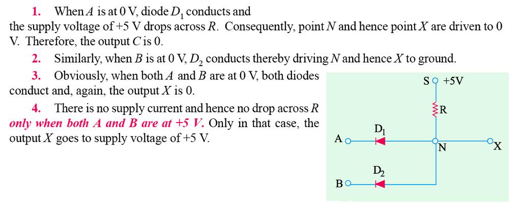
Linear electronic. Lecture No. 1
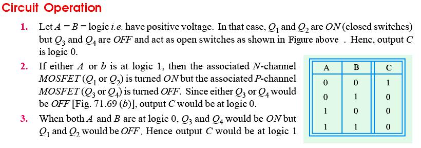
|
|
|
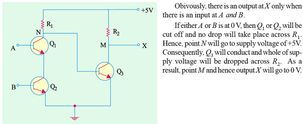
- Helena Brown
- 6 years ago
- Views:
Transcription
1 1 Lecture No. 1
2 2
3 3
4 4
5 5 Lecture No. 2
6 6
7 7
8 8
9 9
10 10
11 11 Lecture No. 3
12 12
13 13
14 14 Lecture No. 4 Example: find Frequency response analysis for the circuit shown in figure below. Where R S =4kR B1 =8kR B2 =4k R E =3.3kR C =6k R L =4k V CC = 12V, I E 1 ma, o = 100, C= 13.9 pf, Cμ = 2 pf, ro =100 kr π = 2.56kC in = C out = 1F, CE=100F. C in C out 1. Mid-Band Gain Calculation R ' L k But R EF = 0
15 15 Linear electronic k 2.4k 100 A v k 4k 1.31k A Vs 2. Low-Frequency Response 15.9Hz 10 4k 6k 2 1 f 6 out 30Hz k 4k 2 1 f 6 in
16 16 2. High-Frequency Response From here up in frequency, we will start to worry about the details of what s inside the BJT. Now those junction capacitances matter, so one needs to use the full Hybrid- model. C total k 208.5pF R ' s Rin Rs 1.31k 4k 987 R R 1.31k 4k in s f h MHz Also, we will discuss other examples and questions
17 17 Lecture No. 5 Multi-stage "Cascaded" Amplifiers Most practical amplifiers required more gain than can be obtain from a single stage. Consequently, it is common practice to feed the output of one amplifier stage into the input of the next stage. Gain and bandwidth considerations in cascaded amplifiers Most of a cascaded amplifier stages are used to obtain either voltage gain or a current gain. However, in most cascaded amplifiers, ultimately the power gain is important. If a voltage gain is required, we can calculate the total gain by using the equation for voltage gain of one stage. Thus, the voltage gain for stage1 is: Vo1 Av1 Vin1 In addition, the voltage gain for stage 2 is: A v2 V V o2 in2 The gain for additional stages can be written in a similar manner. Then, the total amplifier voltage gain A total for n-cascaded stages is: Vo1 Vo 2 V V o3 o(n1) Vo(n 1)... V V V V V in1 o1 o2 on in1 A total A 1 A 2 A 3... A n In same manner, we can derive the current gain or power gain for the cascaded amplifier. Let f 1 and f 2 is the lower and upper cutoff frequencies, respectively. The voltage or current gain of one stage has been reducing to of its reference value at these frequencies. Now, if we have an amplifier with two identical stages of amplification, the voltage gain at f 1 will be reduced by factor of in each stage. Thus, the amplifier gain at f 1 (and also f 2 ) will be: A v A v2 = 0.5 A total
18 18 Linear electronic For n-identical cascaded stages of amplification, the gain at f 1 and f 2 will be (0.707) n A v. The voltage gain per stage is given for the low frequency by: 1 A o j j A 1 o j 1 1 A A The magnitude of above equation is: 2 1 o ) ( 1 1 A A If there are n-cascaded stages, the magnitude of the total gain amplifier is: n 2 1 n o total ) ( 1 1 A A Now, if ω is to be equal to ω L, the term multiplying A o must be equal to.0707 or 1/(2) 1/2. Then n/ 2 2 L 1 1/ L 1 1/n 1 2 Then, 1 2 n / 1 1 L The voltage gain per stage is given for the low frequency by:
19 19 As similar A A H 2 o 2 j 2 2 1/ n 1 From above equations, ω L will be greater than ω 1 if n is greater than one and ω H will be less than ω 2 if n is greater than one. Thus, the bandwidth of the amplifier decreases as the number of cascaded stages increases. On the other hand, if the amplifier bandwidth is to remain constant, the stage bandwidth must increase as the number of cascaded stages increases. Example: If the f 2 =32MHz, A total =1000, and f H = 12MHz, Calculate mid-band gain "A o n " for n=3 & 7 cascaded stages. Determine the gain per stage for each amplifier. ω 2 = 2π ω H = 2π rad/sec rad/sec A total A n o 1 1 ( H 2 ) 2 n 1. For n= A 3 o A o 3 = A o = For n = 7
20 20 A o 7 = A o =2.865
21 21 Lecture No. 6 PRACTICAL CASCADE AMPLIFIER CIRCUIT In the above figure, let us work out the gain assuming nothing about the R in and R out of each stage, looking at them as voltage dividers between each stage and between the last stage and the load. The equation reduces to the ideal case of A V = A 2 for two identical stages if we let the R o 's go to 0 and the R i 's go to infinity. For example: let R o = 100and R in = 1M, what is the gain with two stages of gain A in series? (Assume RL = 1Mtoo).
22 22 By the time you reached that point, other effects would have caused much more trouble (for example, the fact that noise from each successive stage is add to the noise coming into that stage and amplified... on down the line!). Cascode Amplifier Design Example Specifications: DC power dissipation: PD < 25 mw Power Supply: 12 VDC Voltage Gain: -50X Load: Resistive, 50 K Assume R S = 0 Must use 2N2222A Transistors (NPN, ß = 150 measured) DESIGN PROCESS: 1) Pick V cc unless specified.
23 23 2) Calculate I Max. Vcc= 12 VDC 3) Select an I C < I MAX and solve for g m2. Let I C = 1.8 ma 4) Let R S = 0 and solve for R C : R C = 730 5) Use a 1/4, 1/4, 1/4, 1/4 biasing rule to set up bias resistors. Let V CE of the transistors = V cc /4 = 3V and solve the following for R E. 6) The required base current is: 7) Solve for the biasing resistors.
24 24
25 25 Lecture No. 7 FEEDBACK There are two types of feedback: regenerative (positive feedback) and degenerative (negative feedback). Unless you want your circuit to oscillate, we usually use NEGATIVE FEEDBACK... This idea came about in the late 1920 s when they were able to build amplifiers with reasonable gains, but with gains that were difficult to control from amplifier to amplifier... PROPERTIES OF NEGATIVE FEEDBACK Nonlinear distortion can be reduced. The effects of noise can be reduced (but not the noise itself). The input and output impedances of the amplifier can be modified. The bandwidth of an amplifier can be extended. Of course, if you use negative feedback, overall gain of the amplifier is always less than the maximum achievable by the amplifier without feedback. THE BASIC FEEDBACK CIRCUIT With an input signal x s, an output signal x o, a feedback signal x f, and an amplifier input signal x i, let us look at the basic feedback circuit illustrated above.
26 26 The amplifier has a gain of A and the feedback network has a gain of... The input to the amplifier is, x i = x s - x f The output of the amplifier is, x o = A x i We can obtain an expression for the output signal in terms of the input signal and the feedback gain... x o = A x s - x f = A x s - x o Re-arranging, x o = A x s - Ax o x o (1 + A= A x s From which we obtain the negative feedback equation by solving for the overall gain For positive feedback, you only need to change the + sign in the denominator to a - sign. It is easy to obtain the equation for the feedback signal, x f, If the amplifier gain and the loop gain are large (i.e. A>> 1), then the feedback signal x f becomes nearly an identical copy of the input signal x s. Here we have assumed that there was an input comparator or mixer and an output sampler that provided us with a copy of the output signal for use as a feedback signal. The form these devices take depends upon whether the amplifier s input and output are current or voltage based... We refer to a given feedback amplifier in terms of the MIXING - SAMPLING feedback, where MIXING and SAMPLING are either SHUNT or SERIES... There are four possible types... (For sampling think of how you would measure V or I in the lab... series for current and shunt for voltage).
27 27 TYPES OF MIXER TYPES OF SAMPLER
28 28 Lecture No. 8 INPUT-OUTPUT (MIXING - SAMPLING) SERIES-SHUNT series (voltage) mixing, voltage-sampling V-V SHUNT-SERIES shunt (current) mixing, current-sampling, I-I SERIES-SERIES series (voltage) mixing, current-sampling V-I SHUNT-SHUNT shunt (current) mixing, voltage-sampling I-V Let's consider a familiar example... the common-emitter amplifier. Since we sample the output current and generate a voltage feedback signal, this is a series-series feedback topology. Considering the output current to be the output signal (e.g. i o = i c ) and the input to be v s (for simplicity, assume that R B1 and R B2 are very large), the units of the basic amplifier are, We know that the feedback voltage is given by Ohm's Law as, V f =i o R E so the feedback network gain, = R E (NOTE: don't get confused! This is NOT the transistor's!) Transistor's current gain = i o/ v i g m in -1 The output current is given by:
29 29 i o = g m (v s - v f) = g m (v s - i o R E ) Combining these equations to find the overall gain for the amplifier, G m, we end up with an equation we have seen before! Now that: SERIES-SHUNT FEEDBACK (SERIES [VOLTAGE] MIXING, VOLTAGE-SAMPLING) Two examples are shown below. On the left, the common emitter amplifier connect to feedback circuit consist of (R 1 and R 2 ).
30 30 On the right, the non-inverting operation amplifier configuration using an ideal op-amp (infinite input impedance, zero output impedance)... Vcc RL Vo Vin Q1 NPN R1 R2 RE C1 R2 R1 Notice how you can re-draw the two feedback resistors as a feedback network of the form we are discussing. The feedback network gain can be obtained directly by voltage division,
31 31 Lecture No. 9 This can be plugged into the feedback gain equation to find the overall gain, Continuing with the series-shunt case, but including the input and output resistance terms (R i and R o ). We can obtain an expression for the equivalent input and output resistance...
32 32 The output resistance can also be obtained by the same method we used previously: Reduce the input signal (V s ) to zero and apply a test voltage V t at the output. Starting with the definition, Therefore,
33 33 Lecture No. 10 Power Transistor Amplifier Amplifiers are used to increase the level of a signal and, depending on the increase required; stages are often cascaded to increase the gain. The last stage of the cascade may be required to drive same form of load, for example a loudspeaker, a servomechanism or a coaxial cable for RF applications. Power amplifiers are classified by the nature of the collector current waveform into class A, class B and class C. This classification is explained in the following figure, where a typical transfer characteristic of a transistor amplifier is used. CLASS-A AMPLIFIER The simplest possible circuit of a class-a amplifier is shown in Figure below where R L is the load resistance and R B is the biasing resistance.
34 34 We already know that for the maximum undistorted peak-to-peak output voltage swing the Q-point should be selected on the basis of the following equation: In this equation, R DC is the dc resistance and R AC is the ac resistance in the collector-emitter circuit. Thus, R DC = R AC = R L (In circuit above, there is only one resistance) The collector-to-emitter voltage at the operating point is: When the input signal goes negative, it causes a decrease in the collector current and a corresponding increase in the collectorto-emitter voltage. The ac component of the output voltage is now positive. This situation continues until the collector current reaches zero and the collector-to-emitter voltage becomes equal to V CC.
35 35 This is the maximum value of the collector-to-emitter voltage ignoring the nonlinear operation in the cut-off region. From the above discussion, it should become clear that the output voltage is zero when the input signal is zero and the collector voltage is ½ V CC. At that time, the collector current is I CQ. As the collector current becomes 2I CQ, its ac component has a maximum value of I CQ, and the collector-to-emitter voltage is zero. Thus, the ac component of the output voltage has a minimum value of -½V CC. When the collector current becomes zero, the ac component of the collector current has a minimum value of I CQ, and the ac component of the output voltage attains a maximum value of ½ V CC. With this understanding, we can write the timedomain expressions for the total collector current and total collector-to-emitter voltage as: The instantaneous power dissipated by the transistor is: - Where the first term, ½ I CQ V CC, is the power dissipation at the Q- point when there is no input signal. - The second term, ½ I V CC sin 2 (ωt), is due to the input signal. - Figure below shows a plot of the instantaneous power dissipation by the transistor.
36 36 Since the average value of a sin2 (wt) function is ½, the average power dissipated by the transistor, is: The instantaneous power delivered to the load is: Thus, the average power delivered to the load is: We can substitute for I CQ R L = ½ V CC, and obtain an expression for the maximum value of the average power delivered to the load as: The power supplied by the source is: We can determine the efficiency of the class-a amplifier as: Did you notice that the average power dissipated by the transistor at its Q-point is twice as much as the average power output? For this reason, class-a configuration should be used only when the power output is less than or equal to 1 W.
37 37 Lecture No. 11 Example: Design a common-emitter amplifier that delivers 0.5W power to a 100 resistor. Use a transistor that has a maximum current rating of 500mA, collector-to-emitter saturation voltage of 0.5V, breakdown voltage of 40V, and the common-emitter current gain of 100. Solution: Let us first design the common-emitter amplifier. We have selected a four-resistor bias circuit as shown in Figure below because of its stable operation. The average power supplied to the 100-W load resistor is 0.5 W. then; The maximum current through the transistor is expected to be twice as much, i.e. 200mA during the positive excursion of the collector current. Since the transistor can supply a maximum current of 500mA, it is safe to use this transistor. The undistorted maximum output voltage swing is 10 V (100mA100 ). Let us add a 10% safety factor to the current in order to keep the swing from entering the saturation region on one hand and the
38 38 cut-off region on the other. This will help keep the distortion to its minimum. Therefore, let us select, I CQ = 110mA. - We can now determine the supply voltage as: - At the Q-point, the base current is: ICQ 110mA IBQ 1. 1mA Let us select a current in R 2 that is nearly equal to 10 times the base current R Thus, the current through R1: I I IBQ mA 1 2. We can now compute R1: R V cc Vbe k I The power supplied by the dc source, is: Ps ( ICQ I1 ) Vcc ( ) ma W But: P L =0.5W P 0. 5 Then, L % PS PT ( MAX ) VCC ICQ 11110mA 1. 21W 2 In order to determine the voltage gain, current gain, power gain and input resistance, we can represent the circuit in the midfrequency range by its model as shown in Figure below.
39 39 Since the base current is 1.1mA, the equivalent resistance in the base circuit is: V 25 r T IBQ 1. 1 The base current can now be computed as: Where; circuit. is the equivalent resistance in the emitter The collector current is: The output current is: A v V V o in ( 22. 7/ 101)
40 40 R 16.6 in Thus, the current gain: A I = Finally, the power gain is: A P = A V A I A P =(-73.2) (-440) = 32208
41 41 Lecture No. 12 CLASS B AMPLIFIER One of the major disadvantages of a class-a amplifier is that it dissipates maximum power at its Q-point. The amplifier is consuming power even when there is no signal. In fact, the power consumption goes down only when the input signal is present. We can reduce the power consumption just by biasing the transistor at the cutoff point. At the cutoff point, the voltage drop across the transistor is at its maximum value while the current though it is zero. When an amplifier is biased at its cutoff point, it is called the class-b amplifier. Let us consider the situation when the input voltage begins its positive cycle. For the circuit shown, the transistor will not begin to conduct until the input signal is equal to its base-to-emitter voltage drop V BE. As soon as the input voltage goes above V BE, the transistor turns on and the conduction process begins. The output voltage will simply be V IN V BE. As the input voltage increases, the output voltage increases also and so does the current in the collector.
42 42 The average value of the half-wave collector (load) current is: Thus, the power supplied by the dc voltage source is: The effective (rms) value of the load current is: The power supplied to the load is: It is clear that the efficiency is proportional to the amplitude of
43 43 the collector current. Thus, efficiency would be maximum when I O(Peak) = I ACM. V Then; I CC ACM RL Thus, the maximum power supplied by the dc voltage source is: The maximum power delivered to the load is: We can now compute the maximum efficiency of the class-b amplifier as: The power dissipated by the transistor can be obtained by: Differentiating this equation with respect to I O(Peak) and setting it equal to zero, we obtain the peak value of the collector current that results in maximum power dissipation in the transistor. Example A class-b amplifier of the type shown in Figure below drives a load of 100. It operates from a 15-V dc supply. Assume that the base-to-emitter turn on voltage is essentially zero, is very large, and the output voltage is basically sinusoidal. 1- What is the maximum power it can deliver to the load when its collector-to-emitter saturation voltage is 0.5 V? 2- Efficiency. 3- The average and maximum power dissipated by the transistor.
44 44 Solution: When the base-to-emitter turn on voltage (V BE ) is neglected, the transistor turns on as soon as the input voltage becomes positive. Taking into account the collector-to-emitter saturation [V CE(SAT) ] voltage of 0.5 V into account, the maximum possible output voltage is: The maximum value of the load (collector) current is: The average and rms values of the load current are: The power supplied by the 15-V dc source is: The maximum power delivered to the load is: The efficiency of the class-b amplifier is: The average power dissipated by the transistor is: The maximum power dissipation by the transistor is:
45 45 Lecture No. 13 CLASS-B PUSH-PULL AMPLIFIER As explained in the previous section, the class-b amplifier is better than the class-a amplifier because it has high efficiency. However, the class-b amplifier can only amplify the positive-half of the input signal. In order to be able to amplify the entire signal, we can use two complementary transistors as shown in Figure below. When the input signal is positive, the NPN transistor Q1 turns ON, the PNP transistor Q2 is OFF, and the output voltage is positive. The NPN transistor is pushing the current into the load resistor during the positive cycle of the input voltage. The output voltage can be expressed as: The maximum value of the output voltage is obtained during the positive cycle when the NPN transistor just begins to saturate. That is,
46 46 And As the input voltage falls below V BE, the PNP transistor Q 2 begins to conduct and it pulls the current from the load. The NPN transistor Q 1 pushes the current into the load and the PNP transistor Q 2 pulls the current through it. This is why this circuit configuration is referred to as the Push-Pull amplifier. As the PNP transistor, Q 2 turns ON, the NPN transistor Q 1 cuts off and the output voltage is negative. The saturation voltage of the PNP transistor limits the minimum value of the output voltage. Since we are using the two complementary transistors, we expect the magnitude of the saturation voltage for both transistors to be the same. That is V EC(SAT) of the PNP transistor is equal to V CE(SAT) of the NPN transistor. Thus, the minimum value of the output voltage is: And Let us denote the amplitude (the magnitude of the maximum possible swing) of each output waveform as: The maximum current through each transistor is: The average current through each transistor is:
47 47 Example A class-b push-pull amplifier drives a load of 100. It operates from a dual ± 15V dc supply. Assume that the base-to-emitter turn on voltage is zero, is very large, and the output voltage is essentially sinusoidal. 1- What is the maximum power it can deliver to the load when the collector-to-emitter saturation voltage for each transistor is 0.5 V? 2- Efficiency of power transistor amplifier. Solution: The maximum, unclipped peak-to-peak output voltage that we can obtain from the push-pull amplifier is 29 V. The maximum power delivered to the load is: The total power supplied by the 15-V and the 15 V dc sources is: The efficiency of the class-b amplifier is:


48 48 Lecture No. 14 Logic gates A logic gates is an electronic circuit which make decisions. It has one output and one or more inputs. 1. NOT-Gate It is so called because its output is NOT the same as its input. It is also called inverter because it inverts the input. It has one input and one output as shown in figure below. Figure below


49 49 2. OR-gate The output of this circuit is logic "1" when either one input is logic "1" as shown in figure below. Figure Figure

50 50 AND-gate
51 51
52 52
53 53
54 54
55 55
56 56
55:041 Electronic Circuits The University of Iowa Fall Exam 3. Question 1 Unless stated otherwise, each question below is 1 point.
 Exam 3 Name: Score /65 Question 1 Unless stated otherwise, each question below is 1 point. 1. An engineer designs a class-ab amplifier to deliver 2 W (sinusoidal) signal power to an resistive load. Ignoring
Small signal Amplifier stages. Figure 5.2 Classification of power amplifiers
 5.1 Introduction When the power requirement to drive the load is in terms of several Watts rather than mili-watts the power amplifiers are used. Power amplifiers form the last stage of multistage amplifiers.
SIDDHARTH GROUP OF INSTITUTIONS :: PUTTUR (AUTONOMOUS) Siddharth Nagar, Narayanavanam Road QUESTION BANK
 Siddharth Nagar, Narayanavanam Road QUESTION BANK") SIDDHARTH GROUP OF INSTITUTIONS :: PUTTUR (AUTONOMOUS) Siddharth Nagar, Narayanavanam Road 517583 QUESTION BANK Subject with Code : Electronic Circuit Analysis (16EC407) Year & Sem: II-B.Tech & II-Sem
SIDDHARTH GROUP OF INSTITUTIONS :: PUTTUR (AUTONOMOUS) Siddharth Nagar, Narayanavanam Road 517583 QUESTION BANK Subject with Code : Electronic Circuit Analysis (16EC407) Year & Sem: II-B.Tech & II-Sem
Code No: R Set No. 1
 Code No: R059210404 Set No. 1 II B.Tech I Semester Supplimentary Examinations, February 2008 ELECTRONIC CIRCUIT ANALYSIS ( Common to Electronics & Communication Engineering and Electronics & Telematics)
GATE SOLVED PAPER - IN
 YEAR 202 ONE MARK Q. The i-v characteristics of the diode in the circuit given below are : v -. A v 0.7 V i 500 07 $ = * 0 A, v < 0.7 V The current in the circuit is (A) 0 ma (C) 6.67 ma (B) 9.3 ma (D)
Output Stage and Power Amplifiers
 Microelectronic Circuits Output Stage and ower Amplifiers Slide 1 ntroduction Most of the challenging requirement in the design of the output stage is ower delivery to the load. ower consumption at the
Integrated Circuit: Classification:
 Integrated Circuit: It is a miniature, low cost electronic circuit consisting of active and passive components that are irreparably joined together on a single crystal chip of silicon. Classification:
5.25Chapter V Problem Set
 5.25Chapter V Problem Set P5.1 Analyze the circuits in Fig. P5.1 and determine the base, collector, and emitter currents of the BJTs as well as the voltages at the base, collector, and emitter terminals.
Linear IC s and applications
 Questions and Solutions PART-A Unit-1 INTRODUCTION TO OP-AMPS 1. Explain data acquisition system Jan13 DATA ACQUISITION SYSYTEM BLOCK DIAGRAM: Input stage Intermediate stage Level shifting stage Output
I1 19u 5V R11 1MEG IDC Q7 Q2N3904 Q2N3904. Figure 3.1 A scaled down 741 op amp used in this lab
 Lab 3: 74 Op amp Purpose: The purpose of this laboratory is to become familiar with a two stage operational amplifier (op amp). Students will analyze the circuit manually and compare the results with SPICE.
UNIT I BIASING OF DISCRETE BJT AND MOSFET PART A
 UNIT I BIASING OF DISCRETE BJT AND MOSFET PART A 1. Why do we choose Q point at the center of the load line? 2. Name the two techniques used in the stability of the q point.explain. 3. Give the expression
Lab 2: Discrete BJT Op-Amps (Part I)
") Lab 2: Discrete BJT Op-Amps (Part I) This is a three-week laboratory. You are required to write only one lab report for all parts of this experiment. 1.0. INTRODUCTION In this lab, we will introduce and
Lab 2: Discrete BJT Op-Amps (Part I) This is a three-week laboratory. You are required to write only one lab report for all parts of this experiment. 1.0. INTRODUCTION In this lab, we will introduce and
BJT Circuits (MCQs of Moderate Complexity)
") BJT Circuits (MCQs of Moderate Complexity) 1. The current ib through base of a silicon npn transistor is 1+0.1 cos (1000πt) ma. At 300K, the rπ in the small signal model of the transistor is i b B C r
BJT Circuits (MCQs of Moderate Complexity) 1. The current ib through base of a silicon npn transistor is 1+0.1 cos (1000πt) ma. At 300K, the rπ in the small signal model of the transistor is i b B C r
2. SINGLE STAGE BIPOLAR JUNCTION TRANSISTOR (BJT) AMPLIFIERS
 AMPLIFIERS") 2. SINGLE STAGE BIPOLAR JUNCTION TRANSISTOR (BJT) AMPLIFIERS I. Objectives and Contents The goal of this experiment is to become familiar with BJT as an amplifier and to evaluate the basic configurations
2. SINGLE STAGE BIPOLAR JUNCTION TRANSISTOR (BJT) AMPLIFIERS I. Objectives and Contents The goal of this experiment is to become familiar with BJT as an amplifier and to evaluate the basic configurations
Bipolar Junction Transistors
 Bipolar Junction Transistors Invented in 1948 at Bell Telephone laboratories Bipolar junction transistor (BJT) - one of the major three terminal devices Three terminal devices more useful than two terminal
Page 1 of 7. Power_AmpFal17 11/7/ :14
 ECE 3274 Power Amplifier Project (Push Pull) Richard Cooper 1. Objective This project will introduce two common power amplifier topologies, and also illustrate the difference between a Class-B and a Class-AB
Amplifier Frequency Response, Feedback, Oscillations; Op-Amp Block Diagram and Gain-Bandwidth Product
 Amplifier Frequency Response, Feedback, Oscillations; Op-Amp Block Diagram and Gain-Bandwidth Product Physics116A,12/4/06 Draft Rev. 1, 12/12/06 D. Pellett 2 Negative Feedback and Voltage Amplifier AB
Document Name: Electronic Circuits Lab. Facebook: Twitter:
 Document Name: Electronic Circuits Lab www.vidyathiplus.in Facebook: www.facebook.com/vidyarthiplus Twitter: www.twitter.com/vidyarthiplus Copyright 2011-2015 Vidyarthiplus.in (VP Group) Page 1 CIRCUIT
Code: 9A Answer any FIVE questions All questions carry equal marks *****
 II B. Tech II Semester (R09) Regular & Supplementary Examinations, April/May 2012 ELECTRONIC CIRCUIT ANALYSIS (Common to EIE, E. Con. E & ECE) Time: 3 hours Max Marks: 70 Answer any FIVE questions All
Electronic Devices. Floyd. Chapter 7. Ninth Edition. Electronic Devices, 9th edition Thomas L. Floyd
 Electronic Devices Ninth Edition Floyd Chapter 7 Power Amplifiers A power amplifier is a large signal amplifier that produces a replica of the input signal on its output. In the case shown here, the output
Power Amplifiers. Class B Class AB
 ower Amplifiers Class B Class AB Class B he circuit each transistor conducts for a half of every signal period complementary pair push-pull arrangement peration vi ( 0.6; 0.6) (off), (off) v 0 vi v 0.6
INSTITUTE OF AERONAUTICAL ENGINEERING (AUTONOMUS) Dundigal, Hyderabad
 Dundigal, Hyderabad") INSTITUTE OF AERONAUTICAL ENGINEERING (AUTONOMUS) Dundigal, Hyderabad - 00 0 ELECTRONICS AND COMMUNICATION ENGINEERING ASSIGNMENT Name : ELECTRONIC CIRCUIT ANALYSIS Code : A0 Class : II - B. Tech nd semester
INSTITUTE OF AERONAUTICAL ENGINEERING (AUTONOMUS) Dundigal, Hyderabad - 00 0 ELECTRONICS AND COMMUNICATION ENGINEERING ASSIGNMENT Name : ELECTRONIC CIRCUIT ANALYSIS Code : A0 Class : II - B. Tech nd semester
MAHALAKSHMI ENGINEERING COLLEGE TIRUCHIRAPALLI
 MAHALAKSHMI ENGINEERING COLLEGE TIRUCHIRAPALLI-621213. QUESTION BANK DEPARTMENT: EEE SUBJECT CODE: EE2203 SEMESTER : III SUBJECT NAME: ELECTRONIC DEVICES &CIRCUITS UNIT 4-AMPLIFIERS AND OSCILLATORS PART
Chapter 13 Output Stages and Power Amplifiers
 Chapter 13 Output Stages and Power Amplifiers 13.1 General Considerations 13.2 Emitter Follower as Power Amplifier 13.3 Push-Pull Stage 13.4 Improved Push-Pull Stage 13.5 Large-Signal Considerations 13.6
Electronics Lab. (EE21338)
") Princess Sumaya University for Technology The King Abdullah II School for Engineering Electrical Engineering Department Electronics Lab. (EE21338) Prepared By: Eng. Eyad Al-Kouz October, 2012 Table of
Princess Sumaya University for Technology The King Abdullah II School for Engineering Electrical Engineering Department Electronics Lab. (EE21338) Prepared By: Eng. Eyad Al-Kouz October, 2012 Table of
Homework Assignment 12
 Homework Assignment 12 Question 1 Shown the is Bode plot of the magnitude of the gain transfer function of a constant GBP amplifier. By how much will the amplifier delay a sine wave with the following
CHARACTERIZATION OF OP-AMP
 EXPERIMENT 4 CHARACTERIZATION OF OP-AMP OBJECTIVES 1. To sketch and briefly explain an operational amplifier circuit symbol and identify all terminals. 2. To list the amplifier stages in a typical op-amp
Electronics Prof D. C. Dube Department of Physics Indian Institute of Technology, Delhi
 Electronics Prof D. C. Dube Department of Physics Indian Institute of Technology, Delhi Module No. # 04 Feedback in Amplifiers, Feedback Configurations and Multi Stage Amplifiers Lecture No. # 03 Input
Frequency Response of Common Emitter Amplifier
 Başkent University Department of Electrical and Electronics Engineering EEM 311 Electronics II Experiment 6 Frequency Response of Common Emitter Amplifier Aim: The aim of this experiment is to study the
UNIT- IV ELECTRONICS
 UNIT- IV ELECTRONICS INTRODUCTION An operational amplifier or OP-AMP is a DC-coupled voltage amplifier with a very high voltage gain. Op-amp is basically a multistage amplifier in which a number of amplifier
Unit WorkBook 4 Level 4 ENG U19 Electrical and Electronic Principles LO4 Digital & Analogue Electronics 2018 Unicourse Ltd. All Rights Reserved.
 Pearson BTEC Levels 4 Higher Nationals in Engineering (RQF) Unit 19: Electrical and Electronic Principles Unit Workbook 4 in a series of 4 for this unit Learning Outcome 4 Digital & Analogue Electronics
UNIT 1 MULTI STAGE AMPLIFIES
 UNIT 1 MULTI STAGE AMPLIFIES 1. a) Derive the equation for the overall voltage gain of a multistage amplifier in terms of the individual voltage gains. b) what are the multi-stage amplifiers? 2. Describe
(a) BJT-OPERATING MODES & CONFIGURATIONS
 BJT-OPERATING MODES & CONFIGURATIONS") (a) BJT-OPERATING MODES & CONFIGURATIONS 1. The leakage current I CBO flows in (a) The emitter, base and collector leads (b) The emitter and base leads. (c) The emitter and collector leads. (d) The base
(a) BJT-OPERATING MODES & CONFIGURATIONS 1. The leakage current I CBO flows in (a) The emitter, base and collector leads (b) The emitter and base leads. (c) The emitter and collector leads. (d) The base
Oscillators. An oscillator may be described as a source of alternating voltage. It is different than amplifier.
 Oscillators An oscillator may be described as a source of alternating voltage. It is different than amplifier. An amplifier delivers an output signal whose waveform corresponds to the input signal but
Small signal ac equivalent circuit of BJT
 UNIT-2 Part A 1. What is an ac load line? [N/D 16] A dc load line gives the relationship between the q-point and the transistor characteristics. When capacitors are included in a CE transistor circuit,
Index. Small-Signal Models, 14 saturation current, 3, 5 Transistor Cutoff Frequency, 18 transconductance, 16, 22 transit time, 10
 Index A absolute value, 308 additional pole, 271 analog multiplier, 190 B BiCMOS,107 Bode plot, 266 base-emitter voltage, 16, 50 base-emitter voltages, 296 bias current, 111, 124, 133, 137, 166, 185 bipolar
MAHALAKSHMI ENGINEERING COLLEGE TIRUCHIRAPALLI UNIT I FEEDBACK AMPLIFIERS PART A (2 Marks)
") MAHALAKSHMI ENGINEERING COLLEGE TIRUCHIRAPALLI-621213. UNIT I FEEDBACK AMPLIFIERS PART A (2 Marks) 1. Name the types of feedback amplifiers. (AUC MAY 13, DEC06) Voltage Series feedback amplifier Voltage
MAHALAKSHMI ENGINEERING COLLEGE TIRUCHIRAPALLI-621213. UNIT I FEEDBACK AMPLIFIERS PART A (2 Marks) 1. Name the types of feedback amplifiers. (AUC MAY 13, DEC06) Voltage Series feedback amplifier Voltage
Chapter 5 Transistor Bias Circuits
 Chapter 5 Transistor Bias Circuits Objectives Discuss the concept of dc biasing of a transistor for linear operation Analyze voltage-divider bias, base bias, and collector-feedback bias circuits. Basic
Assist Lecturer: Marwa Maki. Active Filters
 Active Filters In past lecture we noticed that the main disadvantage of Passive Filters is that the amplitude of the output signals is less than that of the input signals, i.e., the gain is never greater
Skyup's Media ELECTRONIC CIRCUIT ANALYSIS
 ELECTRONIC CIRCUIT ANALYSIS MALLAREDDY COLLEGE OF ENGINEERING AND TECHNOLOGY DEPARTMENT OF ELECTROINICS AND COMMUNICATION ENGINEERING Answer all the following questions: PART A: B.TECH II YEAR II SEMESTER
Output Stages and Power Amplifiers
 CHAPTER 11 Output Stages and Power Amplifiers Introduction 11.7 Power BJTs 911 11.1 Classification of Output Stages 11. Class A Output Stage 913 11.3 Class B Output Stage 918 11.4 Class AB Output Stage
Electronic Circuits EE359A
 Electronic Circuits EE359A Bruce McNair B206 bmcnair@stevens.edu 201-216-5549 Lecture 4 0 Bipolar Junction Transistors (BJT) Small Signal Analysis Graphical Analysis / Biasing Amplifier, Switch and Logic
Electronic Devices. Floyd. Chapter 6. Ninth Edition. Electronic Devices, 9th edition Thomas L. Floyd
 Electronic Devices Ninth Edition Floyd Chapter 6 Agenda BJT AC Analysis Linear Amplifier AC Load Line Transistor AC Model Common Emitter Amplifier Common Collector Amplifier Common Base Amplifier Special
ESE319 Introduction to Microelectronics High Frequency BJT Model & Cascode BJT Amplifier
 High Frequency BJT Model & Cascode BJT Amplifier 1 Gain of 10 Amplifier Non-ideal Transistor C in R 1 V CC R 2 v s Gain starts dropping at > 1MHz. Why! Because of internal transistor capacitances that
Emitter base bias. Collector base bias Active Forward Reverse Saturation forward Forward Cut off Reverse Reverse Inverse Reverse Forward
 SEMICONDUCTOR PHYSICS-2 [Transistor, constructional characteristics, biasing of transistors, transistor configuration, transistor as an amplifier, transistor as a switch, transistor as an oscillator] Transistor
Physics 116A Notes Fall 2004
 Physics 116A Notes Fall 2004 David E. Pellett Draft v.0.9 beta Notes Copyright 2004 David E. Pellett unless stated otherwise. References: Text for course: Fundamentals of Electrical Engineering, second
BASIC ELECTRONICS PROF. T.S. NATARAJAN DEPT OF PHYSICS IIT MADRAS
 BASIC ELECTRONICS PROF. T.S. NATARAJAN DEPT OF PHYSICS IIT MADRAS LECTURE-12 TRANSISTOR BIASING Emitter Current Bias Thermal Stability (RC Coupled Amplifier) Hello everybody! In our series of lectures
UNIT - 1 OPERATIONAL AMPLIFIER FUNDAMENTALS
 UNIT - 1 OPERATIONAL AMPLIFIER FUNDAMENTALS 1.1 Basic operational amplifier circuit- hte basic circuit of an operational amplifier is as shown in above fig. has a differential amplifier input stage and
Electronic Circuits. Power Amplifiers. Manar Mohaisen Office: F208 Department of EECE
 Electronic Circuits Power Amplifiers Manar Mohaisen Office: F208 Email: manar.subhi@kut.ac.kr Department of EECE Review of the Precedent Lecture Explain the Amplifier Operation Explain the BJT AC Models
HOME ASSIGNMENT. Figure.Q3
 HOME ASSIGNMENT 1. For the differential amplifier circuit shown below in figure.q1, let I=1 ma, V CC =5V, v CM = -2V, R C =3kΩ and β=100. Assume that the BJTs have v BE =0.7 V at i C =1 ma. Find the voltage
In a cascade configuration, the overall voltage and current gains are given by:
 ECE 3274 Two-Stage Amplifier Project 1. Objective The objective of this lab is to design and build a direct coupled two-stage amplifier, including a common-source gain stage and a common-collector buffer
 Pg: 1 VALLIAMMAI ENGINEERING COLLEGE SRM Nagar, Kattankulathur 603 203 Department of Electronics & Communication Engineering Regulation: 2013 Acadamic Year : 2015 2016 EC6304 Electronic Circuits I Question
By: Dr. Ahmed ElShafee
 Lecture (04) Transistor Bias Circuit 3 BJT Amplifiers 1 By: Dr. Ahmed ElShafee ١ Emitter Feedback Bias If an emitter resistor is added to the base bias circuit in Figure, the result is emitter feedback
Analog Electronic Circuits Code: EE-305-F
 Analog Electronic Circuits Code: EE-305-F 1 INTRODUCTION Usually Called Op Amps Section -C Operational Amplifier An amplifier is a device that accepts a varying input signal and produces a similar output
BASIC ELECTRONICS PROF. T.S. NATARAJAN DEPT OF PHYSICS IIT MADRAS
 BASIC ELECTRONICS PROF. T.S. NATARAJAN DEPT OF PHYSICS IIT MADRAS LECTURE-13 Basic Characteristic of an Amplifier Simple Transistor Model, Common Emitter Amplifier Hello everybody! Today in our series
Unit WorkBook 1 Level 4 ENG U22 Electronic Circuits and Devices 2018 UniCourse Ltd. All Rights Reserved. Sample
 Pearson BTEC Level 4 Higher Nationals in Engineering (RQF) Unit 22: Electronic Circuits and Devices Unit Workbook 1 in a series of 4 for this unit Learning Outcome 1 Operational Amplifiers Page 1 of 23
PESIT BANGALORE SOUTH CAMPUS BASIC ELECTRONICS
 PESIT BANGALORE SOUTH CAMPUS QUESTION BANK BASIC ELECTRONICS Sub Code: 17ELN15 / 17ELN25 IA Marks: 20 Hrs/ Week: 04 Exam Marks: 80 Total Hours: 50 Exam Hours: 03 Name of Faculty: Mr. Udoshi Basavaraj Module
EXAM Amplifiers and Instrumentation (EE1C31)
") DELFT UNIVERSITY OF TECHNOLOGY Faculty of Electrical Engineering, Mathematics and Computer Science EXAM Amplifiers and Instrumentation (EE1C31) April 18, 2017, 9.00-12.00 hr This exam consists of four
DELFT UNIVERSITY OF TECHNOLOGY Faculty of Electrical Engineering, Mathematics and Computer Science EXAM Amplifiers and Instrumentation (EE1C31) April 18, 2017, 9.00-12.00 hr This exam consists of four
Chapter 6. BJT Amplifiers
 Basic Electronic Devices and Circuits EE 111 Electrical Engineering Majmaah University 2 nd Semester 1432/1433 H Chapter 6 BJT Amplifiers 1 Introduction The things you learned about biasing a transistor
Miniproject: AM Radio
 Objective UNIVERSITY OF CALIFORNIA AT BERKELEY College of Engineering Department of Electrical Engineering and Computer Sciences EE05 Lab Experiments Miniproject: AM Radio Until now, the labs have focused
Course Number Section. Electronics I ELEC 311 BB Examination Date Time # of pages. Final August 12, 2005 Three hours 3 Instructor
 Course Number Section Electronics ELEC 311 BB Examination Date Time # of pages Final August 12, 2005 Three hours 3 nstructor Dr. R. Raut M aterials allowed: No Yes X (Please specify) Calculators allowed:
I C I E =I B = I C 1 V BE 0.7 V
 Guide to NPN Amplifier Analysis Jason Woytowich 1. Transistor characteristics A BJT has three operating modes cutoff, active, and saturation. For applications, like amplifiers, where linear characteristics
Homework Assignment 11
 Homework Assignment 11 Question 1 (Short Takes) Two points each unless otherwise indicated. 1. What is the 3-dB bandwidth of the amplifier shown below if r π = 2.5K, r o = 100K, g m = 40 ms, and C L =
Week 12: Output Stages, Frequency Response
 ELE 2110A Electronic Circuits Week 12: Output Stages, Frequency esponse (2 hours only) Lecture 12-1 Output Stages Topics to cover Amplifier Frequency esponse eading Assignment: Chap 15.3, 16.1 of Jaeger
Communication Circuit Lab Manual
 German Jordanian University School of Electrical Engineering and IT Department of Electrical and Communication Engineering Communication Circuit Lab Manual Experiment 2 Tuned Amplifier Eng. Anas Alashqar
Experiment 1: Amplifier Characterization Spring 2019
 Experiment 1: Amplifier Characterization Spring 2019 Objective: The objective of this experiment is to develop methods for characterizing key properties of operational amplifiers Note: We will be using
Experiment No. 9 DESIGN AND CHARACTERISTICS OF COMMON BASE AND COMMON COLLECTOR AMPLIFIERS
 Experiment No. 9 DESIGN AND CHARACTERISTICS OF COMMON BASE AND COMMON COLLECTOR AMPLIFIERS 1. Objective: The objective of this experiment is to explore the basic applications of the bipolar junction transistor
Transistor Configuration
 Transistor Configuration 1 Objectives To review BJT biasing circuit. To study BJT amplifier circuit To understand the BJT configuration. To analyse single-stage BJT amplifier circuits. To study the differential
Chapter 6: Power Amplifiers
 Chapter 6: Power Amplifiers Contents Class A Class B Class C Power Amplifiers Class A, B and C amplifiers are used in transmitters Tuned with a band width wide enough to pass all information sidebands
So far we have dealt with only small-signal ampliers. In small-signal ampliers the main factors were amplication linearity gain
 Contents Power Amplier Types Class A Operation Class B Operation Class AB Operation Class C Operation Class D Operation Amplier Eciency Series-Fed Class A Amplier AC-DC Load Lines Maximum Eciency Figure
The George Washington University School of Engineering and Applied Science Department of Electrical and Computer Engineering ECE 20 - LAB
 The George Washington University School of Engineering and Applied Science Department of Electrical and Computer Engineering ECE 20 - LAB Experiment # 6 (Part I) Bipolar Junction Transistors Common Emitter
Electronic Troubleshooting. Chapter 5 Multistage Amplifiers
 Electronic Troubleshooting Chapter 5 Multistage Amplifiers Overview When more amplification is required than can be supplied by a single stage amp A second stage is added Or more stages are added Aspects
ECE 3274 Common-Emitter Amplifier Project
 ECE 3274 Common-Emitter Amplifier Project 1. Objective The objective of this lab is to design and build the common-emitter amplifier with partial bypass of the emitter resistor to control the AC voltage
Module 4 Unit 4 Feedback in Amplifiers
 Module 4 Unit 4 Feedback in mplifiers eview Questions:. What are the drawbacks in a electronic circuit not using proper feedback? 2. What is positive feedback? Positive feedback is avoided in amplifier
DC Bias. Graphical Analysis. Script
 Course: B.Sc. Applied Physical Science (Computer Science) Year & Sem.: Ist Year, Sem - IInd Subject: Electronics Paper No.: V Paper Title: Analog Circuits Lecture No.: 3 Lecture Title: Analog Circuits
SUMMER 13 EXAMINATION Subject Code: Model Answer Page No: / N
 Important Instructions to examiners: 1) The answers should be examined by key words and not as word-to-word as given in the model answer scheme. 2) The model answer and the answer written by candidate
Microelectronic Circuits
 SECOND EDITION ISHBWHBI \ ' -' Microelectronic Circuits Adel S. Sedra University of Toronto Kenneth С Smith University of Toronto HOLT, RINEHART AND WINSTON HOLT, RINEHART AND WINSTON, INC. New York Chicago
Lab 5: Multi-Stage Amplifiers
 UNIVERSITY OF CALIFORNIA AT BERKELEY College of Engineering Department of Electrical Engineering and Computer Sciences EE105 Lab Experiments Lab 5: Multi-Stage Amplifiers Contents 1 Introduction 1 2 Pre-Lab
Basic electronics Prof. T.S. Natarajan Department of Physics Indian Institute of Technology, Madras Lecture- 17. Frequency Analysis
 Basic electronics Prof. T.S. Natarajan Department of Physics Indian Institute of Technology, Madras Lecture- 17 Frequency Analysis Hello everybody! In our series of lectures on basic electronics learning
Lecture 9 Transistors
 Lecture 9 Transistors Physics Transistor/transistor logic CMOS logic CA 1947 http://www.extremetech.com/extreme/164301-graphenetransistors-based-on-negative-resistance-could-spell-theend-of-silicon-and-semiconductors
3-Stage Transimpedance Amplifier
 3-Stage Transimpedance Amplifier ECE 3400 - Dr. Maysam Ghovanloo Garren Boggs TEAM 11 Vasundhara Rawat December 11, 2015 Project Specifications and Design Approach Goal: Design a 3-stage transimpedance
Solid State Devices & Circuits. 18. Advanced Techniques
 ECE 442 Solid State Devices & Circuits 18. Advanced Techniques Jose E. Schutt-Aine Electrical l&c Computer Engineering i University of Illinois jschutt@emlab.uiuc.edu 1 Darlington Configuration - Popular
ECEN 474/704 Lab 6: Differential Pairs
 ECEN 474/704 Lab 6: Differential Pairs Objective Design, simulate and layout various differential pairs used in different types of differential amplifiers such as operational transconductance amplifiers
Chip Name Min VolT. Max Volt. Min. Out Power Typ. Out Power. LM386N-1 4 Volts 12 Volts 250 mw 325 mw. LM386N-3 4 Volts 12 Volts 500 mw 700 mw
 LM386 Audio Amplifier Analysis The LM386 Voltage Audio Power Amplifier by National Semiconductor and also manufactured by JRC/NJM, is an old chip (mid 70 s) that has been a popular choice for low-power
Physics 623 Transistor Characteristics and Single Transistor Amplifier Sept. 12, 2017
 Physics 623 Transistor Characteristics and Single Transistor Amplifier Sept. 12, 2017 1 Purpose To measure and understand the common emitter transistor characteristic curves. To use the base current gain
Fundamentals of Microelectronics. Bipolar Amplifier
 Bipolar Amplifier Voltage Amplifier Performance Metrics - There are many metrics that are used to evaluate how good an amplifier is (1) (Voltage) Gain= Vout/ Vin. Can be found from small-signal 10 8 6
PREVIEW COPY. Amplifiers. Table of Contents. Introduction to Amplifiers...3. Single-Stage Amplifiers...19
 Amplifiers Table of Contents Lesson One Lesson Two Lesson Three Introduction to Amplifiers...3 Single-Stage Amplifiers...19 Amplifier Performance and Multistage Amplifiers...35 Lesson Four Op Amps...51
Electronic Circuits for Mechatronics ELCT 609 Lecture 5: BJT Voltage Amplifiers
 Electronic Circuits for Mechatronics ELCT 609 Lecture 5: BJT Voltage Amplifiers Assistant Professor Office: C3.315 E-mail: eman.azab@guc.edu.eg 1 BJT Modes of Operation Electrical Equations of BJT 2 BJT
Lab 4. Transistor as an amplifier, part 2
 Lab 4 Transistor as an amplifier, part 2 INTRODUCTION We continue the bi-polar transistor experiments begun in the preceding experiment. In the common emitter amplifier experiment, you will learn techniques
BJT Amplifier. Superposition principle (linear amplifier)
") BJT Amplifier Two types analysis DC analysis Applied DC voltage source AC analysis Time varying signal source Superposition principle (linear amplifier) The response of a linear amplifier circuit excited
BJT Amplifier Two types analysis DC analysis Applied DC voltage source AC analysis Time varying signal source Superposition principle (linear amplifier) The response of a linear amplifier circuit excited
A 3-STAGE 5W AUDIO AMPLIFIER
 ECE 2201 PRELAB 7x BJT APPLICATIONS A 3-STAGE 5W AUDIO AMPLIFIER UTILIZING NEGATIVE FEEDBACK INTRODUCTION Figure P7-1 shows a simplified schematic of a 3-stage audio amplifier utilizing three BJT amplifier
Field Effect Transistors
 Field Effect Transistors Purpose In this experiment we introduce field effect transistors (FETs). We will measure the output characteristics of a FET, and then construct a common-source amplifier stage,
Low Distortion Design 3
 Low Distortion Design 3 TIPL 1323 TI Precision Labs Op Amps Presented by Collin Wells Prepared by John Caldwell Prerequisites: Noise 1 3 (TIPL1311 TIPL1313) Output Stage Topologies Most op amps use a Class-AB
EE 332 Design Project
 EE 332 Design Project Variable Gain Audio Amplifier TA: Pohan Yang Students in the team: George Jenkins Mohamed Logman Dale Jackson Ben Alsin Instructor s Comments: Lab Grade: Introduction The goal of
ELECTRONIC CIRCUITS. Time: Three Hours Maximum Marks: 100
 EC 40 MODEL TEST PAPER - 1 ELECTRONIC CIRCUITS Time: Three Hours Maximum Marks: 100 Answer five questions, taking ANY TWO from Group A, any two from Group B and all from Group C. All parts of a question
Exercise 2: AC Voltage and Power Gains
 Exercise 2: AC Voltage and Power Gains When you have completed this exercise, you will be able to determine voltage and power gains by using oscilloscope. The ac operation schematic for the COMPLEMENTARY
Objective: To study and verify the functionality of a) PN junction diode in forward bias. Sl.No. Name Quantity Name Quantity 1 Diode
 PN junction diode in forward bias. Sl.No. Name Quantity Name Quantity 1 Diode") Experiment No: 1 Diode Characteristics Objective: To study and verify the functionality of a) PN junction diode in forward bias Components/ Equipments Required: b) Point-Contact diode in reverse bias Components
Experiment No: 1 Diode Characteristics Objective: To study and verify the functionality of a) PN junction diode in forward bias Components/ Equipments Required: b) Point-Contact diode in reverse bias Components
EE 3305 Lab I Revised July 18, 2003
 Operational Amplifiers Operational amplifiers are high-gain amplifiers with a similar general description typified by the most famous example, the LM741. The LM741 is used for many amplifier varieties
GOVERNMENT OF KARNATAKA KARNATAKA STATE PRE-UNIVERSITY EDUCATION EXAMINATION BOARD II YEAR PUC EXAMINATION JULY-2012 SCHEME OF VALUATION
 GOVERNMENT OF KARNATAKA KARNATAKA STATE PRE-UNIVERSITY EDUCATION EXAMINATION BOARD II YEAR PUC EXAMINATION JULY-0 SCHEME OF VALUATION Subject Code: 40 Subject: PART - A 0. Which region of the transistor
 Code No: Y0221/R07 Set No. 1 I B.Tech Supplementary Examinations, Apr/May 2013 BASIC ELECTRONIC DEVICES AND CIRCUITS (Electrical & Electronics Engineering) Time: 3 hours Max Marks: 80 Answer any FIVE Questions