Electronic Devices. Floyd. Chapter 7. Ninth Edition. Electronic Devices, 9th edition Thomas L. Floyd
|
|
|
- Allison Richardson
- 6 years ago
- Views:
Transcription

1 Electronic Devices Ninth Edition Floyd Chapter 7
2 Power Amplifiers A power amplifier is a large signal amplifier that produces a replica of the input signal on its output. In the case shown here, the output is an inverted replica of the input. V in V out 0 0 A v Generally power amplifiers are defined as those in which it is necessary to consider the problem of heat dissipation (about 1 W or more).
3 Class A Power Amplifiers A class A power amplifier is a large signal amplifier that operates in the linear region. Ideally, a class A amplifier is designed to operate in I C the center of the ac load I c(sat) line. Notice that a class A amplifier dissipates dc power even with no signal. The dc power dissipated is the product of I CQ and V CEQ. I CQ 0 AC load line Q DC load line V CEQ V ce(cutoff) V CE
4 Class A Power Amplifier Efficiency Power gain is the ratio of the power delivered to the load to the input power. The maximum signal power delivered to a load cannot be greater than 0.5 I CQ V CEQ. Class A power amplifiers are not particularly efficient, so they are restricted to low power applications. The maximum theoretical efficiency for a class A amplifier is 0.25 (or 25%) and usually they are considerably less. What is the efficiency of an amplifier that delivers 200 mw to a load if the power supply is 12 V at 400 ma? 6.7%
5
6

7
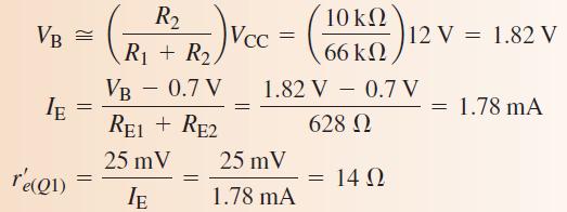
8 Class A Power Amplifier (a) If a 3 V pp signal is applied to the input, what voltage do you expect to see at the speaker? (b) What power is delivered? (a) The CC amplifier has a gain of nearly 1. The output voltage is nearly equal to the input = 3 V pp. (b) The power delivered to the speaker is: 2 V ( 1.06 V ) 2 rms P = = R 8 Ω = 140 mw V in C µ F R 1 10 kω R 2 22 kω V CC +12 V Q 1 Q 2 R E 22 Ω 2 W C µ F V ou t Speaker 8 Ω
9 Class A Power Amplifier For the 3 V pp input, what is the input power and what is the power gain? Assume the Darlington β = 10,000. ( ) V R CC in( tot) = R1 R2 β RE RL +12 V R in( tot) = 6.15 kω 2 V ( 1.06 V ) 2 rms R Pin = = 1 C 1 10 kω Rin ( tot) 6.15 kω V in Q 1 = mw 0.22 µ F Q 2 The power gain is: C 2 R R 2 2 in( tot) kω A 22 kω p = Av = 1 R E RL 8 Ω 22 Ω 2 W = 769 Note that this is approximately 140 mw/0.183 mw 100 µ F V ou t Speaker 8 Ω

10 Class A Power Amplifier The circuit in the previous example can be simulated in Multisim as a check. The input trace (red) and output trace (blue) are nearly identical as expected.
11 Push-Pull Amplifiers Push-pull amplifiers use two transistors working together. One conducts on the positive half cycle; the other conducts on the negative half cycle. This is class B operation. Input transformer Q 1 npn Output transformer V s V CC V out Q 2 npn
12
13 Push-Pull Amplifiers By adding a forward biased diode, the base-emitter drop of the transistors does not need to be overcome by the signal. This is class AB operation. V CC Q 1 npn V s V CC R L V out Q 2 npn Notice that both transistors are npn types.
14 Push-Pull Amplifiers V CC A complementary symmetry push-pull amplifier uses an npn and a pnp transistor working together on alternate half-cycles. The two diodes cause the transistors to Q be biased into slight conduction. 2 V s Because of the slight conduction, this R 2 is also class AB operation and the transistors conduct slightly more than V CC ½ of the input cycle. What is the advantage of class AB operation over class B operation? Cross-over distortion is eliminated. R 1 D 1 D 2 Q 1 R L
15 Push-Pull Amplifiers The ac load line for the npn transistor of a complementary push-pull amplifier is shown. Notice that the Q point is near the right end of the load line. I c(sat) is determined by the load resistor and is given by: I c( sat) V = R CC L I c I c(sat) I CQ I C AC load line V ce V CEQ Q-point V CE
16 Push-Pull Amplifiers Draw the ac load line for the npn transistor. V CC +15 V The ac load line is drawn between I c(sat) and V CC. R Ω D 1 Q 1 I C D A V S R Ω Q 2 R L 30 Ω +15 V V CE V CC 15 V
17 Push-Pull Amplifiers The maximum peak output voltage is always less than the power supply voltage. For the amplifier shown, the peak output will be about +10 V because at the peak of the input, maximum bias current is required. For a given load resistor, you can make the peak output larger by using smaller bias resistors or higher beta transistors (such as Darlington transistors). V S R Ω D 1 D 2 R Ω V CC +15 V V CC Q 1 Q 2 15 V R L 30 Ω
18 Push-Pull Amplifiers Although the complementary symmetry push-pull amplifier as shown here has good power gain and efficiency, it does not have any voltage gain. R Ω D 1 V CC +15 V Q 1 D 2 Why isn t voltage gain possible? Each transistor is configured as a CC amplifier. V S R Ω V CC Q 2 15 V R L 30 Ω
19 Push-Pull Amplifiers V CC +15 V Here, Darlington transistors have replaced the single transistors, the bias resistor are larger (less power dissipation) and two more diodes are added. The maximum output can be larger due to the Darlington transistors despite the larger bias resistors. R 1 D 1 V in D kω D 3 D 4 V out R L 30 Ω Why are four diodes used in this circuit? R kω There are two base-emitter drops for each polarity of the input. V CC 15 V
20 Push-Pull Amplifiers The circuit here is in the lab manual and uses a dc coupled CE amplifier stage to drive the push-pull stage. In this case, the CE amplifier is in the bias path for the push-pull stage. +V CC +9.0 V How would you adjust R 5 for an optimum setting? Monitor the dc output voltage and adjust it for 0 V. V s C µf R 3 68 kω R 5 5 kω R 1 10 kω D 1 1N914 D 2 1N914 Q 3 2N3904 Q 1 2N V Q 2 2N3906 V out R L 330 Ω R 2 10 kω R kω V CC 9.0 V
21 Class C Amplifiers Class C amplifiers are biased into conduction much less than 180 o. They are usually used in RF applications, such as RF oscillators and modulators. The transistor is on when the input signal exceeds V BB + V BE. Because class C amplifiers are biased on for a small percentage of time, they can be very efficient. C +V CC R C V out R B V in V BB
22 Class C Amplifiers Class C operation is useful in oscillators. The collector circuit has a parallel resonant circuit ( tank ) and oscillations are sustained by the short pulse of collector current on each cycle. +V CC I c L C 2 C 3 C 1 V out V out V in R B V BB
23 Class C Amplifiers The circuit can be set up with clamping bias, where the bias resistor is connected to ground. C 1 will charge (through the base-emitter diode) to 0.7 V less than the positive peak. +V CC Clamping action causes the transistor to be cut off except at the positive peak of the input. The R 1 C 1 time constant needs to be long compared to the period of the signal. V p V p V V p Q conducts Q conducts V p 0.7 V + C 1 R 1 C 2 Q L

24 Troubleshooting V S R 1 V CC +15 V Assume a newly constructed push-pull amplifier shows only the lower part of the ac signal at the output. How should you find the problem? 510 Ω You might decide to start with dc Q 1 measurements. D 1 Checking the dc voltages, you find 3.0 V D 2 This is not the expected reading! Q 2 Can you figure out a likely problem? 0.0 V +15 V R Ω R L 30 Ω Diode D 2 is likely to be open. Remove it an test it. 15 V V CC 15 V
25 Selected Key Terms Class A Power gain Efficiency Class B A type of amplifier that operates entirely in its linear (active) region. The ratio of output power to the input power of an amplifier. The ratio of the signal power delivered to a load to the power from the power supply of an amplifier. A type of amplifier that operates in the linear region for 180 o of the input cycle because it is biased at cutoff.
26 Quiz 1. A class A amplifier is designed to operate in the linear region a. for only a small portion of the input cycle b. for ½ of the input cycle c. for slightly more than ½ of the input cycle d. all of the time
27 Quiz 2. A class AB amplifier is designed to operate in the linear region a. for slightly less than ½ of the input cycle b. for exactly ½ of the input cycle c. for slightly more than ½ of the input cycle d. all of the time
28 Quiz 3. Class A power amplifiers a. are not subject to cross-over distortion b. are more efficient than class B amplifiers c. are biased into slight conduction d. all of the above
29 Quiz 4. In a class AB power amplifier, the Q point is ideally a. in the center of the load line b. near the left side of the load line c. near the right side of the load line
30 Quiz 5. The class of operation for the amplifier shown is a. A b. B c. C Input transformer Q 1 npn Output transformer d. AB V s V CC V out Q 2 npn
31 Quiz 6. If R 1 and R 2, are made smaller, the maximum peak output voltage will be a. smaller R Ω V CC +15 V Q 1 b. larger D 1 c. unchanged V S D 2 R Ω Q 2 R L 30 Ω V CC 15 V
32 Quiz 7. The amplifier shown has a. voltage gain V CC +15 V b. current gain c. both of the above R Ω D 1 Q 1 d. none of the above V S D 2 R Ω Q 2 R L 30 Ω V CC 15 V
33 Quiz V CC +15 V 8. The amplifier shown has the advantage of R kω a. high voltage gain D 1 b. no input loading c. excellent power gain V in D 2 D 3 D 4 V out R L 30 Ω d. all of the above R kω V CC 15 V
34 Quiz 9. Ideally the dc voltage at the load with no input signal should be a. 9.0 V b. 0 V c V d V V s C µf R 3 68 kω R 5 5 kω R 1 10 kω D 1 1N914 D 2 1N914 Q 3 2N3904 +V CC +9.0 V Q 1 2N3904 Q 2 2N3906 V out R L 330 Ω R 2 10 kω R kω V CC 9.0 V
35 Quiz 10. The bias type shown is a. clamping bias +V CC b. clipping bias c. emitter bias V p d. base bias Q V p V V p Q conducts Q conducts V p 0.7 V + C 1 R 1 C 2 L
36 Quiz Answers: 1. d 6. b 2. c 7. b 3. a 8. c 4. c 9. b 5. b 10. a
Electronic Circuits. Power Amplifiers. Manar Mohaisen Office: F208 Department of EECE
 Electronic Circuits Power Amplifiers Manar Mohaisen Office: F208 Email: manar.subhi@kut.ac.kr Department of EECE Review of the Precedent Lecture Explain the Amplifier Operation Explain the BJT AC Models
Electronic Devices. Floyd. Chapter 6. Ninth Edition. Electronic Devices, 9th edition Thomas L. Floyd
 Electronic Devices Ninth Edition Floyd Chapter 6 Agenda BJT AC Analysis Linear Amplifier AC Load Line Transistor AC Model Common Emitter Amplifier Common Collector Amplifier Common Base Amplifier Special
DC Bias. Graphical Analysis. Script
 Course: B.Sc. Applied Physical Science (Computer Science) Year & Sem.: Ist Year, Sem - IInd Subject: Electronics Paper No.: V Paper Title: Analog Circuits Lecture No.: 3 Lecture Title: Analog Circuits
Electronic Devices, 9th edition Thomas L. Floyd. Input signal. R 1 and R 2 are selected to establish V B. If the V CE
 3/9/011 lectronic Devices Ninth dition Floyd hapter 5: Transistor ias ircuits The D Operating Point ias establishes the operating point (Q-point) of a transistor amplifier; the ac signal (ma) moves above
Power Amplifiers. Class B Class AB
 ower Amplifiers Class B Class AB Class B he circuit each transistor conducts for a half of every signal period complementary pair push-pull arrangement peration vi ( 0.6; 0.6) (off), (off) v 0 vi v 0.6
LABORATORY MODULE. Analog Electronics. Semester 2 (2005/2006)
") LABORATORY MODULE ENT 162 Analog Electronics Semester 2 (2005/2006) EXPERIMENT 5 : The Class A Common-Emitter Power Amplifier Name Matrix No. : : PUSAT PENGAJIAN KEJURUTERAAN MEKATRONIK KOLEJ UNIVERSITI
LABORATORY MODULE ENT 162 Analog Electronics Semester 2 (2005/2006) EXPERIMENT 5 : The Class A Common-Emitter Power Amplifier Name Matrix No. : : PUSAT PENGAJIAN KEJURUTERAAN MEKATRONIK KOLEJ UNIVERSITI
Chapter 12 Power Amplifier
 Chapter 12 Power Amplifier Definitions In small-signal amplifiers the main factors are: Amplification Linearity Gain Since large-signal, or power, amplifiers handle relatively large voltage signals and
Lecture #9 Tuned Amplifiers
 December 2014 Ahmad El-Banna Integrated Technical Education Cluster At AlAmeeria J-601-1448 Electronic Principals Lecture #9 Tuned Amplifiers Instructor: Dr. Ahmad El-Banna Agenda Class C vs. Tuned Amplifier
EXPERIMENT 5 CURRENT AND VOLTAGE CHARACTERISTICS OF BJT
 EXPERIMENT 5 CURRENT AND VOLTAGE CHARACTERISTICS OF BJT 1. OBJECTIVES 1.1 To practice how to test NPN and PNP transistors using multimeter. 1.2 To demonstrate the relationship between collector current
Lecture (10) Power Amplifiers (2)
 Power Amplifiers (2)") Lecture (10) Power Amplifiers (2) By: Dr. Ahmed ElShafee ١ Class B/AB Power the ideal maximum peak output current for both dual supply and single supply push pull amplifiers is approximately Ic(sat), and
Lecture (10) Power Amplifiers (2) By: Dr. Ahmed ElShafee ١ Class B/AB Power the ideal maximum peak output current for both dual supply and single supply push pull amplifiers is approximately Ic(sat), and
Small signal Amplifier stages. Figure 5.2 Classification of power amplifiers
 5.1 Introduction When the power requirement to drive the load is in terms of several Watts rather than mili-watts the power amplifiers are used. Power amplifiers form the last stage of multistage amplifiers.
SIDDHARTH GROUP OF INSTITUTIONS :: PUTTUR (AUTONOMOUS) Siddharth Nagar, Narayanavanam Road QUESTION BANK
 Siddharth Nagar, Narayanavanam Road QUESTION BANK") SIDDHARTH GROUP OF INSTITUTIONS :: PUTTUR (AUTONOMOUS) Siddharth Nagar, Narayanavanam Road 517583 QUESTION BANK Subject with Code : Electronic Circuit Analysis (16EC407) Year & Sem: II-B.Tech & II-Sem
SIDDHARTH GROUP OF INSTITUTIONS :: PUTTUR (AUTONOMOUS) Siddharth Nagar, Narayanavanam Road 517583 QUESTION BANK Subject with Code : Electronic Circuit Analysis (16EC407) Year & Sem: II-B.Tech & II-Sem
ITT Technical Institute. ET215 Devices 1. Unit 6 Chapter 3, Sections
 ITT Technical Institute ET215 Devices 1 Unit 6 Chapter 3, Sections 3.7-3.9 Chapter 3 Section 3.7 The Bipolar Transistor as a Switch Objectives: Explain how a transistor can be used as a switch 1. Compute
Exercise 2: AC Voltage and Power Gains
 Exercise 2: AC Voltage and Power Gains When you have completed this exercise, you will be able to determine voltage and power gains by using oscilloscope. The ac operation schematic for the COMPLEMENTARY
When you have completed this exercise, you will be able to determine the ac operating characteristics of
 When you have completed this exercise, you will be able to determine the ac operating characteristics of multimeter and an oscilloscope. A sine wave generator connected between the transistor and ground
Chapter 6. BJT Amplifiers
 Basic Electronic Devices and Circuits EE 111 Electrical Engineering Majmaah University 2 nd Semester 1432/1433 H Chapter 6 BJT Amplifiers 1 Introduction The things you learned about biasing a transistor
Crystal Oscillator. Circuit symbol
 Crystal Oscillator Crystal Oscillator Piezoelectric crystal (quartz) Operates as a resonant circuit Shows great stability in oscillation frequency Piezoelectric effect : When mechanical stress is applied
Chapter 6: Power Amplifiers
 Chapter 6: Power Amplifiers Contents Class A Class B Class C Power Amplifiers Class A, B and C amplifiers are used in transmitters Tuned with a band width wide enough to pass all information sidebands
Transistors and Applications
 Chapter 17 Transistors and Applications DC Operation of Bipolar Junction Transistors (BJTs) The bipolar junction transistor (BJT) is constructed with three doped semiconductor regions separated by two
Code No: R Set No. 1
 Code No: R059210404 Set No. 1 II B.Tech I Semester Supplimentary Examinations, February 2008 ELECTRONIC CIRCUIT ANALYSIS ( Common to Electronics & Communication Engineering and Electronics & Telematics)
Page 1 of 7. Power_AmpFal17 11/7/ :14
 ECE 3274 Power Amplifier Project (Push Pull) Richard Cooper 1. Objective This project will introduce two common power amplifier topologies, and also illustrate the difference between a Class-B and a Class-AB
UNIVERSITY OF UTAH ELECTRICAL ENGINEERING DEPARTMENT
 UNIVERSITY OF UTAH ELECTRICAL ENGINEERING DEPARTMENT ECE 3110 LAB EXPERIMENT NO. 4 CLASS AB POWER OUTPUT STAGE Objective: In this laboratory exercise you will build and characterize a class AB power output
Linear electronic. Lecture No. 1
 1 Lecture No. 1 2 3 4 5 Lecture No. 2 6 7 8 9 10 11 Lecture No. 3 12 13 14 Lecture No. 4 Example: find Frequency response analysis for the circuit shown in figure below. Where R S =4kR B1 =8kR B2 =4k R
Lecture 8 Power Amplifier (Class A)
") Lecture 8 Power Amplifier (Class A) nduction of Power Amplifier Power and Efficiency Amplifier Classification Basic Class A Amplifier Transformer Coupled Class A Amplifier Ref:08037HKN EE3110 Power Amplifier
Lecture 8 Power Amplifier (Class A) nduction of Power Amplifier Power and Efficiency Amplifier Classification Basic Class A Amplifier Transformer Coupled Class A Amplifier Ref:08037HKN EE3110 Power Amplifier
Chapter 11 Output Stages
 1 Chapter 11 Output Stages Learning Objectives 2 1) The classification of amplifier output stages 2) Analysis and design of a variety of output-stage types 3) Overview of power amplifiers Introduction
The collector terminal is common to the input and output signals and is connected to the dc power supply. Common Collector Circuit
 Common Collector Circuit When you have completed this exercise, you will be able to determine the dc operating conditions of a common collector (CC) transistor circuit by using a typical CC circuit. You
So far we have dealt with only small-signal ampliers. In small-signal ampliers the main factors were amplication linearity gain
 Contents Power Amplier Types Class A Operation Class B Operation Class AB Operation Class C Operation Class D Operation Amplier Eciency Series-Fed Class A Amplier AC-DC Load Lines Maximum Eciency Figure
Bipolar Junction Transistors
 Bipolar Junction Transistors Invented in 1948 at Bell Telephone laboratories Bipolar junction transistor (BJT) - one of the major three terminal devices Three terminal devices more useful than two terminal
Chapter 5 Transistor Bias Circuits
 Chapter 5 Transistor Bias Circuits Objectives Discuss the concept of dc biasing of a transistor for linear operation Analyze voltage-divider bias, base bias, and collector-feedback bias circuits. Basic
Lab 4. Transistor as an amplifier, part 2
 Lab 4 Transistor as an amplifier, part 2 INTRODUCTION We continue the bi-polar transistor experiments begun in the preceding experiment. In the common emitter amplifier experiment, you will learn techniques
Output Stage and Power Amplifiers
 Microelectronic Circuits Output Stage and ower Amplifiers Slide 1 ntroduction Most of the challenging requirement in the design of the output stage is ower delivery to the load. ower consumption at the
Document Name: Electronic Circuits Lab. Facebook: Twitter:
 Document Name: Electronic Circuits Lab www.vidyathiplus.in Facebook: www.facebook.com/vidyarthiplus Twitter: www.twitter.com/vidyarthiplus Copyright 2011-2015 Vidyarthiplus.in (VP Group) Page 1 CIRCUIT
10. SINGLE-SUPPLY PUSH-PULL AMPLIFIER
 0. SNGE-SUY USH-U AMFE The push-pull amplifier circuit as discussed in section-9 requires a dual power supply. t can be tailored to operate on a single supply as illustrated in Figure 0.. n this case the
A 3-STAGE 5W AUDIO AMPLIFIER
 ECE 2201 PRELAB 7x BJT APPLICATIONS A 3-STAGE 5W AUDIO AMPLIFIER UTILIZING NEGATIVE FEEDBACK INTRODUCTION Figure P7-1 shows a simplified schematic of a 3-stage audio amplifier utilizing three BJT amplifier
Chapter 6: Transistors and Gain
 I. Introduction Chapter 6: Transistors and Gain This week we introduce the transistor. Transistors are three-terminal devices that can amplify a signal and increase the signal s power. The price is that
ECE 334: Electronic Circuits Lecture 2: BJT Large Signal Model
 Faculty of Engineering ECE 334: Electronic Circuits Lecture 2: BJT Large Signal Model Agenda I & V Notations BJT Devices & Symbols BJT Large Signal Model 2 I, V Notations (1) It is critical to understand
... Second Semester
 كنا نظنك اي عيل تركتنا... لكن طيفك مل يزل يغشانا مثل الندى يسقي النبات بقطره... قد ابت ليال يف ادلىج عطشاان ما زلت أذكر حني أدخل معمال... متسك هجازا للقياس تحاكه... فأ راك جتلس هادئا حيرانا تكتب وترمس
BDW93C, BDW94C Series
 Features Designed for general-purpose amplifier and low speed switching applications Collector-emitter sustaining voltage- CEO (sus) = (Minimum) Collector-emitter saturation voltage- CE (sat) = 2 (Maximum)
ET215 Devices I Unit 4A
 ITT Technical Institute ET215 Devices I Unit 4A Chapter 3, Section 3.1-3.2 This unit is divided into two parts; Unit 4A and Unit 4B Chapter 3 Section 3.1 Structure of Bipolar Junction Transistors The basic
Experiment 6: Biasing Circuitry
 1 Objective UNIVERSITY OF CALIFORNIA AT BERKELEY College of Engineering Department of Electrical Engineering and Computer Sciences EE105 Lab Experiments Experiment 6: Biasing Circuitry Setting up a biasing
Designing an Audio Amplifier Using a Class B Push-Pull Output Stage
 Designing an Audio Amplifier Using a Class B Push-Pull Output Stage Angel Zhang Electrical Engineering The Cooper Union for the Advancement of Science and Art Manhattan, NY Jeffrey Shih Electrical Engineering
Experiment 6: Biasing Circuitry
 1 Objective UNIVERSITY OF CALIFORNIA AT BERKELEY College of Engineering Department of Electrical Engineering and Computer Sciences EE105 Lab Experiments Experiment 6: Biasing Circuitry Setting up a biasing
Electronic Troubleshooting
 Electronic Troubleshooting Chapter 3 Bipolar Transistors Most devices still require some individual (discrete) transistors Used to customize operations Interface to external devices Understanding their
BJT Amplifier Power Amp Overview(H.21)
") BJT Amplifier Power Amp Overview(H.21) 20170616-2 Copyright (c) 2016-2017 Young W. Lim. Permission is granted to copy, distribute and/or modify this document under the terms of the GNU Free Documentation
BJT Amplifier Power Amp Overview(H.21) 20170616-2 Copyright (c) 2016-2017 Young W. Lim. Permission is granted to copy, distribute and/or modify this document under the terms of the GNU Free Documentation
Chapter 13 Output Stages and Power Amplifiers
 Chapter 13 Output Stages and Power Amplifiers 13.1 General Considerations 13.2 Emitter Follower as Power Amplifier 13.3 Push-Pull Stage 13.4 Improved Push-Pull Stage 13.5 Large-Signal Considerations 13.6
Chapter 3: Bipolar Junction Transistors
 Chapter 3: Bipolar Junction Transistors Transistor Construction There are two types of transistors: pnp npn pnp The terminals are labeled: E - Emitter B - Base C - Collector npn 2 Transistor Operation
Chapter 4 DC Biasing BJTs. BJTs
 hapter 4 D Biasing BJTs BJTs Biasing Biasing: The D voltages applied to a transistor in order to turn it on so that it can amplify the A signal. Operating Point The D input establishes an operating or
Lecture (05) BJT Amplifiers 2
 BJT Amplifiers 2") Lecture (05) BJT Amplifiers 2 By: Dr. Ahmed ElShafee 1 Effect of the Emitter Bypass Capacitor on Voltage Gain The emitter bypass capacitor, provides an effective short to the ac signal around the emitter
Lecture (05) BJT Amplifiers 2 By: Dr. Ahmed ElShafee 1 Effect of the Emitter Bypass Capacitor on Voltage Gain The emitter bypass capacitor, provides an effective short to the ac signal around the emitter
EXPERIMENT 12: SIMULATION STUDY OF DIFFERENT BIASING CIRCUITS USING NPN BJT
 EXPERIMENT 12: SIMULATION STUDY OF DIFFERENT BIASING CIRCUITS USING NPN BJT AIM: 1) To study different BJT DC biasing circuits 2) To design voltage divider bias circuit using NPN BJT SOFTWARE TOOL: PC
LARGE SIGNAL AMPLIFIERS
 LARGE SIGNAL AMPLIFIERS One method used to distinguish the electrical characteristics of different types of amplifiers is by class, and as such amplifiers are classified according to their circuit configuration
Computer Controlled Curve Tracer
 Computer Controlled Curve Tracer Christopher Curro The Cooper Union New York, NY Email: chris@curro.cc David Katz The Cooper Union New York, NY Email: katz3@cooper.edu Abstract A computer controlled curve
Experiment #6: Biasing an NPN BJT Introduction to CE, CC, and CB Amplifiers
 SCHOOL OF ENGINEERING AND APPLIED SCIENCE DEPARTMENT OF ELECTRICAL AND COMPUTER ENGINEERING ECE 2115: ENGINEERING ELECTRONICS LABORATORY Experiment #6: Biasing an NPN BJT Introduction to CE, CC, and CB
BJT AC Analysis CHAPTER OBJECTIVES 5.1 INTRODUCTION 5.2 AMPLIFICATION IN THE AC DOMAIN
 BJT AC Analysis 5 CHAPTER OBJECTIVES Become familiar with the, hybrid, and hybrid p models for the BJT transistor. Learn to use the equivalent model to find the important ac parameters for an amplifier.
b b Fig. 1 Transistor symbols
 TRANSISTORS Transistors have three terminals which are referred to as emitter (e), base (b) and collector (c). Fig 1 shows the symbols used for the two types of transistors in common use. c c b b e e npn
2. SINGLE STAGE BIPOLAR JUNCTION TRANSISTOR (BJT) AMPLIFIERS
 AMPLIFIERS") 2. SINGLE STAGE BIPOLAR JUNCTION TRANSISTOR (BJT) AMPLIFIERS I. Objectives and Contents The goal of this experiment is to become familiar with BJT as an amplifier and to evaluate the basic configurations
2. SINGLE STAGE BIPOLAR JUNCTION TRANSISTOR (BJT) AMPLIFIERS I. Objectives and Contents The goal of this experiment is to become familiar with BJT as an amplifier and to evaluate the basic configurations
Power Amplifiers. Introduction to Power Amplifiers. Amplifiers. Module
 Module 5 Amplifiers Introduction to What you ll learn in Module 5. Section 5.0 Introduction to. Understand the Operation of. Section 5.1 Power Transistors & Heat Sinks. Power Transistor Construction. Power
Concepts to be Covered
 Introductory Medical Device Prototyping Analog Circuits Part 2 Semiconductors, http://saliterman.umn.edu/ Department of Biomedical Engineering, University of Minnesota Concepts to be Covered Semiconductors
Operational Amplifiers
 Operational Amplifiers November 23, 2017 1 Pre-lab Calculations 1) Calculate the gain for all four circuits in Fig. 3. 2 Introduction Operational Amplifiers? They should call them fun amplifiers. Because,
Lecture 3: Transistors
 Lecture 3: Transistors Now that we know about diodes, let s put two of them together, as follows: collector base emitter n p n moderately doped lightly doped, and very thin heavily doped At first glance,
Experiment No. 9 DESIGN AND CHARACTERISTICS OF COMMON BASE AND COMMON COLLECTOR AMPLIFIERS
 Experiment No. 9 DESIGN AND CHARACTERISTICS OF COMMON BASE AND COMMON COLLECTOR AMPLIFIERS 1. Objective: The objective of this experiment is to explore the basic applications of the bipolar junction transistor
Input and output coupling
 Input and output coupling To overcome the challenge of creating necessary DC bias voltage for an amplifier's input signal without resorting to the insertion of a battery in series with the AC signal source,
I C I E =I B = I C 1 V BE 0.7 V
 Guide to NPN Amplifier Analysis Jason Woytowich 1. Transistor characteristics A BJT has three operating modes cutoff, active, and saturation. For applications, like amplifiers, where linear characteristics
Discrete Op-Amp Kit MitchElectronics 2019
 Discrete Op-Amp Kit MitchElectronics 2019 www.mitchelectronics.co.uk CONTENTS Introduction 3 Schematic 4 How It Works 5 Materials 9 Construction 10 Important Information 11 Page 2 INTRODUCTION Even if
Common Emitter Amplifier
 EE 360 Circuits & Electronics Lab. #5 Common Emitter Amplifier Lab Date: March 28, 2001 Takafumi Asaki Partner: Paola Jaramillo Instructor: R. M. Loftus ABSTRACT By using the basic concept of the NPN transistor,
Chapter 15 Goals. ac-coupled Amplifiers Example of a Three-Stage Amplifier
 Chapter 15 Goals ac-coupled multistage amplifiers including voltage gain, input and output resistances, and small-signal limitations. dc-coupled multistage amplifiers. Darlington configuration and cascode
Darlington Transistors
 Features: Designed for general-purpose amplifier and low speed switching applications Collector-Emitter sustaining voltage V CEO (sus) = 60 V (Minimum) - TIP45 = 80 V (Minimum) - TIP4, TIP46 = 00 V (Minimum)
Low Distortion Design 3
 Low Distortion Design 3 TIPL 1323 TI Precision Labs Op Amps Presented by Collin Wells Prepared by John Caldwell Prerequisites: Noise 1 3 (TIPL1311 TIPL1313) Output Stage Topologies Most op amps use a Class-AB
ELEC 2210 EXPERIMENT 7 The Bipolar Junction Transistor (BJT)
") ELEC 2210 EXPERIMENT 7 The Bipolar Junction Transistor (BJT) Objectives: The experiments in this laboratory exercise will provide an introduction to the BJT. You will use the Bit Bucket breadboarding system
ELEC 2210 EXPERIMENT 7 The Bipolar Junction Transistor (BJT) Objectives: The experiments in this laboratory exercise will provide an introduction to the BJT. You will use the Bit Bucket breadboarding system
Lab 2: Discrete BJT Op-Amps (Part I)
") Lab 2: Discrete BJT Op-Amps (Part I) This is a three-week laboratory. You are required to write only one lab report for all parts of this experiment. 1.0. INTRODUCTION In this lab, we will introduce and
Lab 2: Discrete BJT Op-Amps (Part I) This is a three-week laboratory. You are required to write only one lab report for all parts of this experiment. 1.0. INTRODUCTION In this lab, we will introduce and
Lecture (06) BJT Amplifiers 3
 BJT Amplifiers 3") Lecture (06) BJT Amplifiers 3 By: Dr. Ahmed ElShafee ١ THE COMMON COLLECTOR AMPLIFIER An emitter follower circuit with voltage divider bias is shown in Figure, the input signal is capacitively coupled
Lecture (06) BJT Amplifiers 3 By: Dr. Ahmed ElShafee ١ THE COMMON COLLECTOR AMPLIFIER An emitter follower circuit with voltage divider bias is shown in Figure, the input signal is capacitively coupled
Microelectronics Circuit Analysis and Design. Interdigitated BJT: Top and Cross-Sectional Views. Power Amps 10/11/2013. In this chapter, we will:
 Microelectronics Circuit Analysis and Design Donald A. Neamen Chapter 8 Output Stages and Power Amplifiers In this chapter, we will: Describe the characteristics of BJT and MOSFET power transistors Define
Homework Assignment 12
 Homework Assignment 12 Question 1 Shown the is Bode plot of the magnitude of the gain transfer function of a constant GBP amplifier. By how much will the amplifier delay a sine wave with the following
KOM2751 Analog Electronics :: Dr. Muharrem Mercimek :: YTU - Control and Automation Dept. 1 2 (CONT D - II) DIODE APPLICATIONS
 DIODE APPLICATIONS") KOM2751 Analog Electronics :: Dr. Muharrem Mercimek :: YTU - Control and Automation Dept. 1 2 (CONT D - II) DIODE APPLICATIONS Most of the content is from the textbook: Electronic devices and circuit theory,
KOM2751 Analog Electronics :: Dr. Muharrem Mercimek :: YTU - Control and Automation Dept. 1 2 (CONT D - II) DIODE APPLICATIONS Most of the content is from the textbook: Electronic devices and circuit theory,
Experiment #8: Designing and Measuring a Common-Collector Amplifier
 SCHOOL OF ENGINEERING AND APPLIED SCIENCE DEPARTMENT OF ELECTRICAL AND COMPUTER ENGINEERING ECE 2115: ENGINEERING ELECTRONICS LABORATORY Experiment #8: Designing and Measuring a Common-Collector Amplifier
Chapter 3. Bipolar Junction Transistors
 Chapter 3. Bipolar Junction Transistors Outline: Fundamental of Transistor Common-Base Configuration Common-Emitter Configuration Common-Collector Configuration Introduction The transistor is a three-layer
Lecture 9. Bipolar Junction Transistor (BJT) BJT 1-1
 BJT 1-1") Lecture 9 ipolar Junction Transistor (JT) JT 1-1 Outline ontinue JT JT iasing D analysis Fixed-bias circuit mitter-stabilized bias circuit oltage divider bias circuit D bias with voltage feedback circuit
Lecture 9 ipolar Junction Transistor (JT) JT 1-1 Outline ontinue JT JT iasing D analysis Fixed-bias circuit mitter-stabilized bias circuit oltage divider bias circuit D bias with voltage feedback circuit
Analog Electronics. Electronic Devices, 9th edition Thomas L. Floyd Pearson Education. Upper Saddle River, NJ, All rights reserved.
 Analog Electronics BJT Structure The BJT has three regions called the emitter, base, and collector. Between the regions are junctions as indicated. The base is a thin lightly doped region compared to the
Qualitative analysis of small-signal modified Sziklai pair amplifier
 Indian Journal of Pure & Applied Physics Vol. 50, April 2012, pp. 272-276 Qualitative analysis of small-signal modified Sziklai pair amplifier Beena Pandey, Susmrita Srivastava, Satyendra Nath Tiwari,
Physics 116A Notes Fall 2004
 Physics 116A Notes Fall 2004 David E. Pellett Draft v.0.9 beta Notes Copyright 2004 David E. Pellett unless stated otherwise. References: Text for course: Fundamentals of Electrical Engineering, second
ชาว ศวกรรมคอมพ วเตอร คณะว ศวกรรมศาสตร มหาว ทยาล ยเทคโนโลย ราชมงคลพระนคร
 EN2042102 วงจรไฟฟ าและอ เล กทรอน กส Circuits and Electronics บทท 7 ทรานซ สเตอร Bipolar Junction Transistor สาขาว ชาว ศวกรรมคอมพ วเตอร คณะว ศวกรรมศาสตร มหาว ทยาล ยเทคโนโลย ราชมงคลพระนคร Objectives Describe
PartIIILectures. Multistage Amplifiers
 University of missan Electronic II, Second year 2015-2016 PartIIILectures Assistant Lecture: 1 Multistage and Compound Amplifiers Basic Definitions: 1- Gain of Multistage Amplifier: Fig.(1-1) A general
Code: 9A Answer any FIVE questions All questions carry equal marks *****
 II B. Tech II Semester (R09) Regular & Supplementary Examinations, April/May 2012 ELECTRONIC CIRCUIT ANALYSIS (Common to EIE, E. Con. E & ECE) Time: 3 hours Max Marks: 70 Answer any FIVE questions All
Diode and Bipolar Transistor Circuits
 Diode and Bipolar Transistor Circuits 2 2.1 A Brief Review of Semiconductors Semiconductors are crystalline structures in which each atom shares its valance electrons with the neighboring atoms. The simple
Lecture 14. Bipolar Junction Transistor (BJT) BJT 1-1
 BJT 1-1") Lecture 14 ipolar Junction Transistor (JT) JT 1-1 Outline ontinue JT iasing D analysis Fixed-bias circuit (revision) mitter-stabilized bias circuit oltage divider bias circuit D bias with voltage feedback
Lecture 14 ipolar Junction Transistor (JT) JT 1-1 Outline ontinue JT iasing D analysis Fixed-bias circuit (revision) mitter-stabilized bias circuit oltage divider bias circuit D bias with voltage feedback
Linear IC s and applications
 Questions and Solutions PART-A Unit-1 INTRODUCTION TO OP-AMPS 1. Explain data acquisition system Jan13 DATA ACQUISITION SYSYTEM BLOCK DIAGRAM: Input stage Intermediate stage Level shifting stage Output
EXPERIMENT 10: SINGLE-TRANSISTOR AMPLIFIERS 11/11/10
 EXPERIMENT 10: SINGLE-TRANSISTOR AMPLIFIERS 11/11/10 In this experiment we will measure the characteristics of the standard common emitter amplifier. We will use the 2N3904 npn transistor. If you have
UNIT 1 MULTI STAGE AMPLIFIES
 UNIT 1 MULTI STAGE AMPLIFIES 1. a) Derive the equation for the overall voltage gain of a multistage amplifier in terms of the individual voltage gains. b) what are the multi-stage amplifiers? 2. Describe
Tutorial 2 BJTs, Transistor Bias Circuits, BJT Amplifiers FETs and FETs Amplifiers. Part 1: BJTs, Transistor Bias Circuits and BJT Amplifiers
 Tutorial 2 BJTs, Transistor Bias Circuits, BJT Amplifiers FETs and FETs Amplifiers Part 1: BJTs, Transistor Bias Circuits and BJT Amplifiers 1. Explain the purpose of a thin, lightly doped base region.
EXPERIMENT 10: Power Amplifiers
 EXPERIMENT 10: Power Amplifiers 10.1 Examination Of Class A Amplifier 10.2 Examination Of Class B Amplifier 10.3 Examination Of Class C Amplifier BASIC ELECTRONICS set 15.1 INTRODUCTION There are classes
Lecture 9 Transistors
 Lecture 9 Transistors Physics Transistor/transistor logic CMOS logic CA 1947 http://www.extremetech.com/extreme/164301-graphenetransistors-based-on-negative-resistance-could-spell-theend-of-silicon-and-semiconductors
 Code No: Y0221/R07 Set No. 1 I B.Tech Supplementary Examinations, Apr/May 2013 BASIC ELECTRONIC DEVICES AND CIRCUITS (Electrical & Electronics Engineering) Time: 3 hours Max Marks: 80 Answer any FIVE Questions
(a) BJT-OPERATING MODES & CONFIGURATIONS
 BJT-OPERATING MODES & CONFIGURATIONS") (a) BJT-OPERATING MODES & CONFIGURATIONS 1. The leakage current I CBO flows in (a) The emitter, base and collector leads (b) The emitter and base leads. (c) The emitter and collector leads. (d) The base
(a) BJT-OPERATING MODES & CONFIGURATIONS 1. The leakage current I CBO flows in (a) The emitter, base and collector leads (b) The emitter and base leads. (c) The emitter and collector leads. (d) The base
EEE225: Analogue and Digital Electronics
 EEE225: Analogue and Digital Electronics Lecture II James E. Green Department of Electronic Engineering University of Sheffield j.e.green@sheffield.ac.uk This Lecture 1 One Transistor Circuits Continued...
ClassABampDesign. Do not design for an edge. Class B push pull stage. Vdd = - Vee. For Vin < Vbe (Ri + Rin2) / Rin2
 / Rin2") ClassABampDesign Richard Cooper October 17 2016 When the input signal is positive, the NPN transistor Q1 turns ON, the PNP transistor Q2 is OFF, and the output voltage is positive. The NPN transistor (emitter
ClassABampDesign Richard Cooper October 17 2016 When the input signal is positive, the NPN transistor Q1 turns ON, the PNP transistor Q2 is OFF, and the output voltage is positive. The NPN transistor (emitter
Improving Amplifier Voltage Gain
 15.1 Multistage ac-coupled Amplifiers 1077 TABLE 15.3 Three-Stage Amplifier Summary HAND ANALYSIS SPICE RESULTS Voltage gain 998 1010 Input signal range 92.7 V Input resistance 1 M 1M Output resistance
Experiment 8&9 BJT AMPLIFIER
 Experiment 8&9 BJT AMPLIFIER 1 BJT AS AMPLIFIER 1. Objectiv e: 1- To demonstrate the operation and characteristics of small signals common emitter amplifiers. 2- What do we mean by a linear amplifier and
Darlington Transistor TO-3
 Description Designed for use as output devices in complementary general purpose amplifier applications. Features: High gain darlington performance High DC current gain hfe = 1,000 (Minimum) at Ic = 20A
Darlington Transistors
 Features: Designed for general-purpose amplifier and low speed switching applications Collector-emitter sustaining voltage - V CEO (sus) = 60 V (minimum) - TIP120, TIP125 80 V (minimum) - TIP121, TIP126
Introduction PNP C NPN C
 Introduction JT Transistors: A JT (or any transistor) can be used either as a switch with positions of on or off, or an amplifier that controls its output at all levels in between the extreme on or off
การไบอ สทรานซ สเตอร. Transistors Biasing
 การไบอ สทรานซ สเตอร Transistors iasing iasing iasing: Applying D voltages to a transistor in order to turn it on so that it can amplify A signals. The D input establishes an operating or quiescent point