Transistor Configuration
|
|
|
- Magdalen Chandler
- 5 years ago
- Views:
Transcription
1 Transistor Configuration 1

2 Objectives To review BJT biasing circuit. To study BJT amplifier circuit To understand the BJT configuration. To analyse single-stage BJT amplifier circuits. To study the differential amplifier. To design amplifier circuits. 2
3 Transistor Biasing Circuits Voltage Divider Bias Emitter Bias Base Bias Emitter-feedback Bias Collector-feedback Bias 3
4 Voltage Divider Bias Voltage-divider bias is the most widely used type of bias circuit. Only one power supply is needed and voltage-divider bias is more stable( independent) than other bias types. For this reason it will be the primary focus for study. 4
5 In the case where base to ground resistance(input resistance) is low enough to consider, we can determine it by the simplified equation R IN(base) = DC R E We can view the voltage at point A of the circuit in two ways, with or without the input resistance(point A to ground) considered. 5

6 Thevinizing the bias circuit 6
7 Stiff voltage divider Stiff voltage divider: (No loading effect) 1. I B is much smaller than I 2 2. R IN(BASE) = DC R E >10R 2 V B = (R 2 /(R 1 + R 2 ))V CC I E I C Non-Stiff voltage divider: (with loading effect) V B R 1 R 2 DCR ( R 2 DC E R E V ) CC 7

8 We now take the known base voltage and subtract V BE to find out what is dropped across R E. Knowing the voltage across R E we can apply Ohm s law to determine the current in the collector-emitter side of the circuit. Remember the current in the base-emitter circuit is much smaller, so much in fact we can for all practical purposes we say that I E approximately equals I C. I E I C 8
9 Example Determine the dc input resistance looking at the base of the transistor if DC =
10 Example Determine V CE and I C in the stiff voltage divider biased transistor circuit if DC =
11 Example Find I C and V EC for the pnp transistor circuit as given. 11
12 Example Find I C and V CE for the pnp transistor circuit as given. Assume R 1 =68 kω, R2= 47 kω, R C = 1.8 kω,r E = 2.2 kω, V CC = -6 V and DC =
13 Emitter Bias This type of circuit is independent of making it as stable as the voltage-divider type. The drawback is that it requires two power supplies. Two key equations for analysis of this type of bias circuit are shown below. With these two currents known we can apply Ohm s law and Kirchhoff's law to solve for the voltages. Approximation calculation: V E = V B -V BE -1 V V E = I E R E + V EE I C I E = (-V EE - 1)/R E independent of Precise calculation: I B I E / I C I E (-V EE -V BE )/(R E + R B / DC ) 13
14 Emitter Bias 14
15 15
16 16
17 17
18 Base Bias This type of circuit is very unstable since its changes with temperature and collector current. Base biasing circuits are rarely used in linear circuits and mainly limited to switching applications. KVL around base and collector circuits; -V CC +I B R B +V BE =0 I B = (V CC -V BE )/R B I C = DC I B I C = DC (V CC -V BE )/R B dependent of V CE = V CC -I C R C 18
19 Example Determine how much Q-point(I C and V CE ) for the given circuit will change a over temperature range where DC increases from 100 to 200. Assume V BE = 0.7 V. 19
20 Review Summary(1) The purpose of biasing is to establish a stable operating point (Qpoint). The Q-point is the best point for operation of a transistor for a given collector current. The dc load line helps to establish the Q-point for a given collector current. The linear region of a transistor is the region of operation within saturation and cutoff. 20
21 Review Summary (2) Voltage-divider bias is most widely used because it is stable and uses only one voltage supply. Base bias is very unstable because it is dependent. Emitter bias is stable but require two voltage supplies. Collector-feedback is relatively stable when compared to base bias, but not as stable as voltage-divider bias. 21
22 Summary of Bias Circuits(1) Voltage Divider 22
23 Summary of Bias Circuits(2) Emiiter Bias Base Bias 23
24 Summary of Bias Circuits(3) Collector-feedback Bias Emitter-feedback Bias 24
25 BJT Amplifier One of the primary uses of a transistor is to amplify ac signals. This could be an audio signal or perhaps some high frequency radio signal. It has to be able to do this without distorting the original input. For the analysis of transistor circuits from both dc and ac perspectives, the ac subscripts are lower case and italicized. Instantaneous values use both italicized lower case letters and subscripts. 25
26 Linear Amplifier Recall from the previous chapter that the purpose of dc biasing was to establish the Q-point for operation. The collector curves and load lines help us to relate the Q-point and its proximity to cutoff and saturation. The Q-point is best established where the signal variations do not cause the transistor to go into saturation or cutoff. What we are most interested in is the ac signal itself. Since the dc part of the overall signal is filtered out in most cases, we can view a transistor circuit in terms of just its ac component. 26
27 The boundary between cutoff and saturation is called the linear region. A transistor which operates in the linear region is called a linear amplifier. Note that only the ac component reaches the load because of the capacitive coupling and that the output is 180º out of phase with input. No distortion Note. Subscript Q represents Q-point 27
28 I c(sat) AC load line V ce(cutoff) Graphical operation of the amplifier showing the variation of the base current, collector current, and collectorto-emitter voltage about their dc Q-point values. I b and I c are on different scales. 28
29 Example The ac load line of a certain amplifier extends 10µA above and below Q-point base current value of 50µA as shown. Determine the resulting peak-peak value of I c and V ce.
30 Common-Emitter Amplifier The CE configuration has the emitter as the common terminal, or ground, to an ac signal. The common-emitter amplifier exhibits high voltage and current gain. The output signal is 180º out of phase with the input. Note. The circuit analysis can be done by dc and ac analysis 30
31 CE Amplifier DC Analysis The dc component of the circuit sees only the part of the circuit that is within the boundaries of C 1, C 2, and C 3 as the dc will not pass through these components. The equivalent circuit for dc analysis is shown. The methods for dc analysis are just are the same as dealing with a voltage-divider circuit. Stiff voltage divider or not? [R IN(BASE) > 10R 2 ] 31
32 Example Draw waveforms of V B,V E,I E,V CE 32
33 Darlington Amplifier The darlington pair is used to boost the input impedance to reduce loading of high output impedance circuits. The collectors are joined together and the emitter of the input transistor is connected to the base of the output transistor. The input impedance can be determined the formula below. R in = ac1 ac2 R e 33
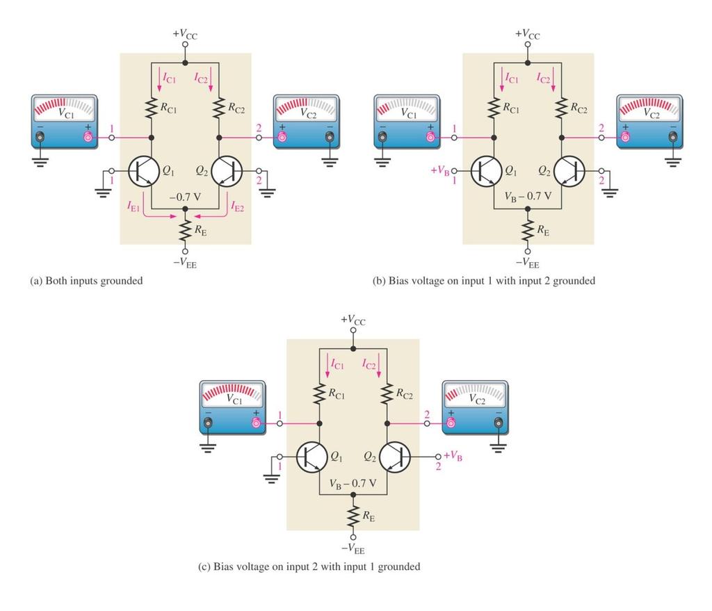
34 A darlington emitter-follower used as a buffer between a common-emitter amplifier and a low-resistance load such as a speaker.

35 Multistage Amplifier Two or more amplifiers can be connected to increase the gain of an ac signal. The overall gain can be calculated by simply multiplying each gain together. A v = A v1 A v2 A v3 Reminder: The term GAIN is used to describe the amplification capability. 35
36 Decibels Amplifier voltage gain is often expressed in decibels(db) A v(db) = 20logA v Each stage s gain can now can be simply added together for the total. 36

37 The capacitive coupling keeps dc bias voltages separate but allows the ac to pass through to the next stage. 37
38 Direct coupling(no coupling or by pass capacitor) between stage improves low frequency gain. The disadvantage is that small changes in dc bias from temperature changes or supply variations becomes more pronounced. Application: Low frequency or dc(0 Hz) amplifier 38
39 Example 1. Whether or not this voltage-divider is stiff? 2. Determine V B V E I E I C and V C 39
40 Example 1. Whether or not this voltage-divider is stiff? 2. Determine V B V E I E I C V C and V CE 40
41 Differential Amplifier Outputs are a function of the difference between two inputs 2 operational modes: differential mode and common mode It is important as a basic of operational amplifiers.(op-amp) 41

42 Basic Differential Amp 42
43

44 Single-ended input operation of differential amplifier
45 Double-ended input operation of differential amplifier
46 Common-mode operation of differential amplifier
47 Example Draw the waveforms of Vout1 and Vout2 47
48 CMRR Common-mode rejection ratio(cmrr) is the measure of an amplifier s ability to reject common-mode signal. It is defined as a ratio of differential voltage gain and common-mode gain. The higher CMRR, the better. CMRR A v( d ) A cm CMRR 20log( A v( d ) A cm ) (in decibel) 48
49 Summary Most transistors amplifiers are designed to operate in the linear region. Transistor circuits can be view in terms of its ac equivalent for better understanding. The common-emitter amplifier has high voltage and current gain. The common-collector has a high current gain and voltage gain of 1. It has a high input impedance and low output impedance. The common-base has a high voltage gain and a current gain of 1. It has a low input impedance and high output impedance Multistage amplifiers are amplifier circuits cascaded to increased gain. We can express gain in decibels (db). 49
50 Supplement
51 Loading Effect V in R total R o + V o - Load side R load The load resistance connected to the potentiometer introduce the error to the output voltage V R R [Unloaded] Without R load, o in [Load] With R load, V o R o o total // R V load ( R R ) R // R total o o load Loading Error: V [ unloaded ] V [ load ] o o V in 51
52 Exercise From a given circuit, the output voltage from the potentiometer is used to drive the load with 100kΩ resistance. As a result, the loading error is applied at the output of the pot. What is the value of loading error in volts??? Explain the method to overcome this problem?? 52

53 Troubleshooting Shown is a typical voltage divider circuit with correct voltage readings. Knowing these voltages is a requirement before logical troubleshooting can be applied. We will discuss some of the faults and symptoms. 53
. Emitter voltage goes down to 0 V. 54")
54 R1 Open With no bias the transistor is in cutoff. Base voltage goes down to 0 V. Collector voltage goes up to 10 V(V CC ). Emitter voltage goes down to 0 V. 54
55 Resistor R E Open: Transistor is in cutoff. Base reading voltage will stay approximately the same. Collector voltage goes up to 10 V(V CC ). Emitter voltage will be approximately the base voltage +.7 V. 55
56 Base Open Internally: Transistor is in cutoff. Base voltage stays approximately the same. Collector voltage goes up to 10 V(V CC ). Emitter voltage goes down to 0 V. 56
Transistor Configuration
 Transistor Configuration 1 Objectives To review BJT biasing circuit. To study BJT amplifier circuit To understand the BJT configuration. To analyse single-stage BJT amplifier circuits. To study the differential
Chapter 5 Transistor Bias Circuits
 Chapter 5 Transistor Bias Circuits Objectives Discuss the concept of dc biasing of a transistor for linear operation Analyze voltage-divider bias, base bias, and collector-feedback bias circuits. Basic
REVIEW TRANSISTOR BIAS CIRCUIT
 EVIEW TANSISTO BIAS CICUIT OBJECTIVES Discuss the concept of dc biasing of a transistor for linear operation Analyze voltage-divider bias, base bias, and collectorfeedback bias circuits. Basic troubleshooting
ET215 Devices I Unit 4A
 ITT Technical Institute ET215 Devices I Unit 4A Chapter 3, Section 3.1-3.2 This unit is divided into two parts; Unit 4A and Unit 4B Chapter 3 Section 3.1 Structure of Bipolar Junction Transistors The basic
DC Bias. Graphical Analysis. Script
 Course: B.Sc. Applied Physical Science (Computer Science) Year & Sem.: Ist Year, Sem - IInd Subject: Electronics Paper No.: V Paper Title: Analog Circuits Lecture No.: 3 Lecture Title: Analog Circuits
Electronic Devices. Floyd. Chapter 6. Ninth Edition. Electronic Devices, 9th edition Thomas L. Floyd
 Electronic Devices Ninth Edition Floyd Chapter 6 Agenda BJT AC Analysis Linear Amplifier AC Load Line Transistor AC Model Common Emitter Amplifier Common Collector Amplifier Common Base Amplifier Special
Tutorial 2 BJTs, Transistor Bias Circuits, BJT Amplifiers FETs and FETs Amplifiers. Part 1: BJTs, Transistor Bias Circuits and BJT Amplifiers
 Tutorial 2 BJTs, Transistor Bias Circuits, BJT Amplifiers FETs and FETs Amplifiers Part 1: BJTs, Transistor Bias Circuits and BJT Amplifiers 1. Explain the purpose of a thin, lightly doped base region.
The collector terminal is common to the input and output signals and is connected to the dc power supply. Common Collector Circuit
 Common Collector Circuit When you have completed this exercise, you will be able to determine the dc operating conditions of a common collector (CC) transistor circuit by using a typical CC circuit. You
Lecture (06) BJT Amplifiers 3
 BJT Amplifiers 3") Lecture (06) BJT Amplifiers 3 By: Dr. Ahmed ElShafee 1 Current Gain 2 Power Gain The overall power gain is the product of the overall voltage gain (Av ) and the overall current gain (Ai). 3 THE COMMON
Lecture (06) BJT Amplifiers 3 By: Dr. Ahmed ElShafee 1 Current Gain 2 Power Gain The overall power gain is the product of the overall voltage gain (Av ) and the overall current gain (Ai). 3 THE COMMON
Electronics Lab. (EE21338)
") Princess Sumaya University for Technology The King Abdullah II School for Engineering Electrical Engineering Department Electronics Lab. (EE21338) Prepared By: Eng. Eyad Al-Kouz October, 2012 Table of
Princess Sumaya University for Technology The King Abdullah II School for Engineering Electrical Engineering Department Electronics Lab. (EE21338) Prepared By: Eng. Eyad Al-Kouz October, 2012 Table of
Module 4 Unit 4 Feedback in Amplifiers
 Module 4 Unit 4 Feedback in mplifiers eview Questions:. What are the drawbacks in a electronic circuit not using proper feedback? 2. What is positive feedback? Positive feedback is avoided in amplifier
ITT Technical Institute. ET215 Devices 1. Unit 6 Chapter 3, Sections
 ITT Technical Institute ET215 Devices 1 Unit 6 Chapter 3, Sections 3.7-3.9 Chapter 3 Section 3.7 The Bipolar Transistor as a Switch Objectives: Explain how a transistor can be used as a switch 1. Compute
When you have completed this exercise, you will be able to determine the ac operating characteristics of
 When you have completed this exercise, you will be able to determine the ac operating characteristics of multimeter and an oscilloscope. A sine wave generator connected between the transistor and ground
Linear IC s and applications
 Questions and Solutions PART-A Unit-1 INTRODUCTION TO OP-AMPS 1. Explain data acquisition system Jan13 DATA ACQUISITION SYSYTEM BLOCK DIAGRAM: Input stage Intermediate stage Level shifting stage Output
... Second Semester
 كنا نظنك اي عيل تركتنا... لكن طيفك مل يزل يغشانا مثل الندى يسقي النبات بقطره... قد ابت ليال يف ادلىج عطشاان ما زلت أذكر حني أدخل معمال... متسك هجازا للقياس تحاكه... فأ راك جتلس هادئا حيرانا تكتب وترمس
CHAPTER 3 THE BIPOLAR JUNCTION TRANSISTOR (BJT)
") HAPT 3 TH IPOLA JUNTION TANSISTO (JT) 1 In this chapter, we will: JT Discuss the physical structure and operation of the bipolar junction transistor. Understand the dc analysis of bipolar transistor circuits.
HAPT 3 TH IPOLA JUNTION TANSISTO (JT) 1 In this chapter, we will: JT Discuss the physical structure and operation of the bipolar junction transistor. Understand the dc analysis of bipolar transistor circuits.
Document Name: Electronic Circuits Lab. Facebook: Twitter:
 Document Name: Electronic Circuits Lab www.vidyathiplus.in Facebook: www.facebook.com/vidyarthiplus Twitter: www.twitter.com/vidyarthiplus Copyright 2011-2015 Vidyarthiplus.in (VP Group) Page 1 CIRCUIT
PartIIILectures. Multistage Amplifiers
 University of missan Electronic II, Second year 2015-2016 PartIIILectures Assistant Lecture: 1 Multistage and Compound Amplifiers Basic Definitions: 1- Gain of Multistage Amplifier: Fig.(1-1) A general
UNIT I BIASING OF DISCRETE BJT AND MOSFET PART A
 UNIT I BIASING OF DISCRETE BJT AND MOSFET PART A 1. Why do we choose Q point at the center of the load line? 2. Name the two techniques used in the stability of the q point.explain. 3. Give the expression
Operational Amplifier BME 360 Lecture Notes Ying Sun
 Operational Amplifier BME 360 Lecture Notes Ying Sun Characteristics of Op-Amp An operational amplifier (op-amp) is an analog integrated circuit that consists of several stages of transistor amplification
Unit WorkBook 1 Level 4 ENG U22 Electronic Circuits and Devices 2018 UniCourse Ltd. All Rights Reserved. Sample
 Pearson BTEC Level 4 Higher Nationals in Engineering (RQF) Unit 22: Electronic Circuits and Devices Unit Workbook 1 in a series of 4 for this unit Learning Outcome 1 Operational Amplifiers Page 1 of 23
Linear electronic. Lecture No. 1
 1 Lecture No. 1 2 3 4 5 Lecture No. 2 6 7 8 9 10 11 Lecture No. 3 12 13 14 Lecture No. 4 Example: find Frequency response analysis for the circuit shown in figure below. Where R S =4kR B1 =8kR B2 =4k R
55:041 Electronic Circuits The University of Iowa Fall Exam 3. Question 1 Unless stated otherwise, each question below is 1 point.
 Exam 3 Name: Score /65 Question 1 Unless stated otherwise, each question below is 1 point. 1. An engineer designs a class-ab amplifier to deliver 2 W (sinusoidal) signal power to an resistive load. Ignoring
I C I E =I B = I C 1 V BE 0.7 V
 Guide to NPN Amplifier Analysis Jason Woytowich 1. Transistor characteristics A BJT has three operating modes cutoff, active, and saturation. For applications, like amplifiers, where linear characteristics
EE 482 Electronics II
 EE 482 Electronics II Lab #4: BJT Differential Pair with Resistive Load Overview The objectives of this lab are (1) to design and analyze the performance of a differential amplifier, and (2) to measure
Assist Lecturer: Marwa Maki. Active Filters
 Active Filters In past lecture we noticed that the main disadvantage of Passive Filters is that the amplitude of the output signals is less than that of the input signals, i.e., the gain is never greater
Electronics EECE2412 Spring 2017 Exam #2
 Electronics EECE2412 Spring 2017 Exam #2 Prof. Charles A. DiMarzio Department of Electrical and Computer Engineering Northeastern University 30 March 2017 File:12198/exams/exam2 Name: : General Rules:
Electronic Devices, 9th edition Thomas L. Floyd. Input signal. R 1 and R 2 are selected to establish V B. If the V CE
 3/9/011 lectronic Devices Ninth dition Floyd hapter 5: Transistor ias ircuits The D Operating Point ias establishes the operating point (Q-point) of a transistor amplifier; the ac signal (ma) moves above
BJT Circuits (MCQs of Moderate Complexity)
") BJT Circuits (MCQs of Moderate Complexity) 1. The current ib through base of a silicon npn transistor is 1+0.1 cos (1000πt) ma. At 300K, the rπ in the small signal model of the transistor is i b B C r
BJT Circuits (MCQs of Moderate Complexity) 1. The current ib through base of a silicon npn transistor is 1+0.1 cos (1000πt) ma. At 300K, the rπ in the small signal model of the transistor is i b B C r
Electronic Troubleshooting
 Electronic Troubleshooting Chapter 3 Bipolar Transistors Most devices still require some individual (discrete) transistors Used to customize operations Interface to external devices Understanding their
Chapter 6. BJT Amplifiers
 Basic Electronic Devices and Circuits EE 111 Electrical Engineering Majmaah University 2 nd Semester 1432/1433 H Chapter 6 BJT Amplifiers 1 Introduction The things you learned about biasing a transistor
Exercise 2: AC Voltage and Power Gains
 Exercise 2: AC Voltage and Power Gains an oscilloscope. Signals of equal magnitude but opposite polarity are needed for each transistor (Q1 and Q2). Center-tapped input transformer T1 is used as a phase
BJT. Bipolar Junction Transistor BJT BJT 11/6/2018. Dr. Satish Chandra, Assistant Professor, P P N College, Kanpur 1
 BJT Bipolar Junction Transistor Satish Chandra Assistant Professor Department of Physics P P N College, Kanpur www.satish0402.weebly.com The Bipolar Junction Transistor is a semiconductor device which
ELC224 Final Review (12/10/2009) Name:
 Name:") ELC224 Final Review (12/10/2009) Name: Select the correct answer to the problems 1 through 20. 1. A common-emitter amplifier that uses direct coupling is an example of a dc amplifier. 2. The frequency
ELC224 Final Review (12/10/2009) Name: Select the correct answer to the problems 1 through 20. 1. A common-emitter amplifier that uses direct coupling is an example of a dc amplifier. 2. The frequency
Lesson number one. Operational Amplifier Basics
 What About Lesson number one Operational Amplifier Basics As well as resistors and capacitors, Operational Amplifiers, or Op-amps as they are more commonly called, are one of the basic building blocks
Transistor Biasing and Operational amplifier fundamentals. OP-amp Fundamentals and its DC characteristics. BJT biasing schemes
 Lab 1 Transistor Biasing and Operational amplifier fundamentals Experiment 1.1 Experiment 1.2 BJT biasing OP-amp Fundamentals and its DC characteristics BJT biasing schemes 1.1 Objective 1. To sketch potential
By: Dr. Ahmed ElShafee
 Lecture (04) Transistor Bias Circuit 3 BJT Amplifiers 1 By: Dr. Ahmed ElShafee ١ Emitter Feedback Bias If an emitter resistor is added to the base bias circuit in Figure, the result is emitter feedback
Engineering Spring Homework Assignment 4: BJT Biasing and Small Signal Properties
 Engineering 1620 -- Spring 2011 Homework Assignment 4: BJT Biasing and Small Signal Properties 1.) The circuit below is a common collector amplifier using constant current biasing. (Constant current biasing
I1 19u 5V R11 1MEG IDC Q7 Q2N3904 Q2N3904. Figure 3.1 A scaled down 741 op amp used in this lab
 Lab 3: 74 Op amp Purpose: The purpose of this laboratory is to become familiar with a two stage operational amplifier (op amp). Students will analyze the circuit manually and compare the results with SPICE.
HOME ASSIGNMENT. Figure.Q3
 HOME ASSIGNMENT 1. For the differential amplifier circuit shown below in figure.q1, let I=1 ma, V CC =5V, v CM = -2V, R C =3kΩ and β=100. Assume that the BJTs have v BE =0.7 V at i C =1 ma. Find the voltage
Phy 335, Unit 4 Transistors and transistor circuits (part one)
") Mini-lecture topics (multiple lectures): Phy 335, Unit 4 Transistors and transistor circuits (part one) p-n junctions re-visited How does a bipolar transistor works; analogy with a valve Basic circuit
Mini-lecture topics (multiple lectures): Phy 335, Unit 4 Transistors and transistor circuits (part one) p-n junctions re-visited How does a bipolar transistor works; analogy with a valve Basic circuit
Code: 9A Answer any FIVE questions All questions carry equal marks *****
 II B. Tech II Semester (R09) Regular & Supplementary Examinations, April/May 2012 ELECTRONIC CIRCUIT ANALYSIS (Common to EIE, E. Con. E & ECE) Time: 3 hours Max Marks: 70 Answer any FIVE questions All
Bipolar Junction Transistors
 Bipolar Junction Transistors Invented in 1948 at Bell Telephone laboratories Bipolar junction transistor (BJT) - one of the major three terminal devices Three terminal devices more useful than two terminal
EE 3111 Lab 7.1. BJT Amplifiers
 EE 3111 Lab 7.1 BJT Amplifiers BJT Amplifier Device/circuit that alters the amplitude of a signal, while keeping input waveform shape BJT amplifiers run the BJT in active mode. Forward current gain is
Lecture #2 Operational Amplifiers
 Spring 2015 Benha University Faculty of Engineering at Shoubra ECE-322 Electronic Circuits (B) Lecture #2 Operational Amplifiers Instructor: Dr. Ahmad El-Banna Agenda Introduction Op-Amps Input Modes and
Exercise 2: AC Voltage and Power Gains
 Exercise 2: AC Voltage and Power Gains When you have completed this exercise, you will be able to determine voltage and power gains by using oscilloscope. The ac operation schematic for the COMPLEMENTARY
SAMPLE FINAL EXAMINATION FALL TERM
 ENGINEERING SCIENCES 154 ELECTRONIC DEVICES AND CIRCUITS SAMPLE FINAL EXAMINATION FALL TERM 2001-2002 NAME Some Possible Solutions a. Please answer all of the questions in the spaces provided. If you need
DHANALAKSHMI COLLEGE OF ENGINEERING DEPARTMENT OF ELECTRICAL AND ELECTRONICS ENGINEERING EC6202 ELECTRONIC DEVICES AND CIRCUITS
 DHANALAKSHMI COLLEGE OF ENGINEERING DEPARTMENT OF ELECTRICAL AND ELECTRONICS ENGINEERING EC6202 ELECTRONIC DEVICES AND CIRCUITS UNIT-I - PN DIODEAND ITSAPPLICATIONS 1. What is depletion region in PN junction?
Electronic Troubleshooting. Chapter 5 Multistage Amplifiers
 Electronic Troubleshooting Chapter 5 Multistage Amplifiers Overview When more amplification is required than can be supplied by a single stage amp A second stage is added Or more stages are added Aspects
Designing an Audio Amplifier Using a Class B Push-Pull Output Stage
 Designing an Audio Amplifier Using a Class B Push-Pull Output Stage Angel Zhang Electrical Engineering The Cooper Union for the Advancement of Science and Art Manhattan, NY Jeffrey Shih Electrical Engineering
Small signal ac equivalent circuit of BJT
 UNIT-2 Part A 1. What is an ac load line? [N/D 16] A dc load line gives the relationship between the q-point and the transistor characteristics. When capacitors are included in a CE transistor circuit,
ECE 334: Electronic Circuits Lecture 2: BJT Large Signal Model
 Faculty of Engineering ECE 334: Electronic Circuits Lecture 2: BJT Large Signal Model Agenda I & V Notations BJT Devices & Symbols BJT Large Signal Model 2 I, V Notations (1) It is critical to understand
Chapter 15 Goals. ac-coupled Amplifiers Example of a Three-Stage Amplifier
 Chapter 15 Goals ac-coupled multistage amplifiers including voltage gain, input and output resistances, and small-signal limitations. dc-coupled multistage amplifiers. Darlington configuration and cascode
UNIVERSITY OF UTAH ELECTRICAL ENGINEERING DEPARTMENT
 UNIVERSITY OF UTAH ELECTRICAL ENGINEERING DEPARTMENT ECE 3110 LAB EXPERIMENT NO. 4 CLASS AB POWER OUTPUT STAGE Objective: In this laboratory exercise you will build and characterize a class AB power output
In a cascade configuration, the overall voltage and current gains are given by:
 ECE 3274 Two-Stage Amplifier Project 1. Objective The objective of this lab is to design and build a direct coupled two-stage amplifier, including a common-source gain stage and a common-collector buffer
GOVERNMENT OF KARNATAKA KARNATAKA STATE PRE-UNIVERSITY EDUCATION EXAMINATION BOARD II YEAR PUC EXAMINATION JULY-2012 SCHEME OF VALUATION
 GOVERNMENT OF KARNATAKA KARNATAKA STATE PRE-UNIVERSITY EDUCATION EXAMINATION BOARD II YEAR PUC EXAMINATION JULY-0 SCHEME OF VALUATION Subject Code: 40 Subject: PART - A 0. Which region of the transistor
Lab 4. Transistor as an amplifier, part 2
 Lab 4 Transistor as an amplifier, part 2 INTRODUCTION We continue the bi-polar transistor experiments begun in the preceding experiment. In the common emitter amplifier experiment, you will learn techniques
EE 3305 Lab I Revised July 18, 2003
 Operational Amplifiers Operational amplifiers are high-gain amplifiers with a similar general description typified by the most famous example, the LM741. The LM741 is used for many amplifier varieties
When you have completed this exercise, you will be able to determine ac operating characteristics of a
 When you have completed this exercise, you will be able to determine ac operating characteristics of a multimeter and an oscilloscope. A sine wave generator connected between the transistor base and ground
Learning Objectives:
 Learning Objectives: At the end of this topic you will be able to; recall the conditions for maximum voltage transfer between sub-systems; analyse a unity gain op-amp voltage follower, used in impedance
Lecture (06) BJT Amplifiers 3
 BJT Amplifiers 3") Lecture (06) BJT Amplifiers 3 By: Dr. Ahmed ElShafee ١ THE COMMON COLLECTOR AMPLIFIER An emitter follower circuit with voltage divider bias is shown in Figure, the input signal is capacitively coupled
Lecture (06) BJT Amplifiers 3 By: Dr. Ahmed ElShafee ١ THE COMMON COLLECTOR AMPLIFIER An emitter follower circuit with voltage divider bias is shown in Figure, the input signal is capacitively coupled
For the purpose of this problem sheet use the model given in the lecture notes.
 Analogue Electronics Questions Todd Huffman & Tony Weidberg, MT 2018 (updated 30/10/18). For the purpose of this problem sheet use the model given in the lecture notes. The current gain is defined by a
Transistor Biasing. DC Biasing of BJT. Transistor Biasing. Transistor Biasing 11/23/2018
 Transistor Biasing DC Biasing of BJT Satish Chandra Assistant Professor Department of Physics P P N College, Kanpur www.satish0402.weebly.com A transistors steady state of operation depends a great deal
LINEAR IC APPLICATIONS
 1 B.Tech III Year I Semester (R09) Regular & Supplementary Examinations December/January 2013/14 1 (a) Why is R e in an emitter-coupled differential amplifier replaced by a constant current source? (b)
Integrated Circuit: Classification:
 Integrated Circuit: It is a miniature, low cost electronic circuit consisting of active and passive components that are irreparably joined together on a single crystal chip of silicon. Classification:
ECEN 474/704 Lab 6: Differential Pairs
 ECEN 474/704 Lab 6: Differential Pairs Objective Design, simulate and layout various differential pairs used in different types of differential amplifiers such as operational transconductance amplifiers
Transistors and Applications
 Chapter 17 Transistors and Applications DC Operation of Bipolar Junction Transistors (BJTs) The bipolar junction transistor (BJT) is constructed with three doped semiconductor regions separated by two
UNIVERSITY OF PENNSYLVANIA EE 206
 UNIVERSITY OF PENNSYLVANIA EE 206 TRANSISTOR BIASING CIRCUITS Introduction: One of the most critical considerations in the design of transistor amplifier stages is the ability of the circuit to maintain
5.25Chapter V Problem Set
 5.25Chapter V Problem Set P5.1 Analyze the circuits in Fig. P5.1 and determine the base, collector, and emitter currents of the BJTs as well as the voltages at the base, collector, and emitter terminals.
EC1203: ELECTRONICS CIRCUITS-I UNIT-I TRANSISTOR BIASING PART-A
 SHRI ANGALAMMAN COLLEGE OF ENGG & TECH., TRICHY 621105 (Approved by AICTE, New Delhi and Affiliated to Anna University Chennai/Trichy) ( ISO 9001:2008 Certified Institution) DEPARTMENT OF ELECTRONICS &
A 3-STAGE 5W AUDIO AMPLIFIER
 ECE 2201 PRELAB 7x BJT APPLICATIONS A 3-STAGE 5W AUDIO AMPLIFIER UTILIZING NEGATIVE FEEDBACK INTRODUCTION Figure P7-1 shows a simplified schematic of a 3-stage audio amplifier utilizing three BJT amplifier
Improving Amplifier Voltage Gain
 15.1 Multistage ac-coupled Amplifiers 1077 TABLE 15.3 Three-Stage Amplifier Summary HAND ANALYSIS SPICE RESULTS Voltage gain 998 1010 Input signal range 92.7 V Input resistance 1 M 1M Output resistance
Lecture (05) BJT Amplifiers 2
 BJT Amplifiers 2") Lecture (05) BJT Amplifiers 2 By: Dr. Ahmed ElShafee 1 Effect of the Emitter Bypass Capacitor on Voltage Gain The emitter bypass capacitor, provides an effective short to the ac signal around the emitter
Lecture (05) BJT Amplifiers 2 By: Dr. Ahmed ElShafee 1 Effect of the Emitter Bypass Capacitor on Voltage Gain The emitter bypass capacitor, provides an effective short to the ac signal around the emitter
By: Dr. Ahmed ElShafee
 Lecture (02) Transistor operating point & DC Load line (2), Transistor Bias Circuit 1 By: Dr. Ahmed ElShafee ١ DC Load Line The dc operation can be described graphically using a dc load line. This is a
ANALOG FUNDAMENTALS C. Topic 4 BASIC FET AMPLIFIER CONFIGURATIONS
 AV18-AFC ANALOG FUNDAMENTALS C Topic 4 BASIC FET AMPLIFIER CONFIGURATIONS 1 ANALOG FUNDAMENTALS C AV18-AFC Overview This topic identifies the basic FET amplifier configurations and their principles of
Chapter 11 Output Stages
 1 Chapter 11 Output Stages Learning Objectives 2 1) The classification of amplifier output stages 2) Analysis and design of a variety of output-stage types 3) Overview of power amplifiers Introduction
ECE 255, Discrete-Circuit Amplifiers
 ECE 255, Discrete-Circuit Amplifiers 20 March 2018 In this lecture, we will continue with the study of transistor amplifiers with the presence of biasing circuits and coupling capacitors in place. We will
Experiment #8: Designing and Measuring a Common-Collector Amplifier
 SCHOOL OF ENGINEERING AND APPLIED SCIENCE DEPARTMENT OF ELECTRICAL AND COMPUTER ENGINEERING ECE 2115: ENGINEERING ELECTRONICS LABORATORY Experiment #8: Designing and Measuring a Common-Collector Amplifier
Electronic Devices. Floyd. Chapter 7. Ninth Edition. Electronic Devices, 9th edition Thomas L. Floyd
 Electronic Devices Ninth Edition Floyd Chapter 7 Power Amplifiers A power amplifier is a large signal amplifier that produces a replica of the input signal on its output. In the case shown here, the output
ECE 3274 Common-Emitter Amplifier Project
 ECE 3274 Common-Emitter Amplifier Project 1. Objective The objective of this lab is to design and build three variations of the common- emitter amplifier. 2. Components Qty Device 1 2N2222 BJT Transistor
Electronic Circuits. Power Amplifiers. Manar Mohaisen Office: F208 Department of EECE
 Electronic Circuits Power Amplifiers Manar Mohaisen Office: F208 Email: manar.subhi@kut.ac.kr Department of EECE Review of the Precedent Lecture Explain the Amplifier Operation Explain the BJT AC Models
BJT AC Analysis CHAPTER OBJECTIVES 5.1 INTRODUCTION 5.2 AMPLIFICATION IN THE AC DOMAIN
 BJT AC Analysis 5 CHAPTER OBJECTIVES Become familiar with the, hybrid, and hybrid p models for the BJT transistor. Learn to use the equivalent model to find the important ac parameters for an amplifier.
EXPT NO: 1.A. COMMON EMITTER AMPLIFIER (Software) PRELAB:
 PRELAB:") EXPT NO: 1.A COMMON EMITTER AMPLIFIER (Software) PRELAB: 1. Study the operation and working principle of CE amplifier. 2. Identify all the formulae you will need in this Lab. 3. Study the procedure of
EXPT NO: 1.A COMMON EMITTER AMPLIFIER (Software) PRELAB: 1. Study the operation and working principle of CE amplifier. 2. Identify all the formulae you will need in this Lab. 3. Study the procedure of
Differential Amplifier Design
 Differential Amplifier Design Design with ideal current source bias. Differential and common mode gain results Add finite output resistance to current source. Replace ideal current source with current
CHAPTER 3: BIPOLAR JUNCION TRANSISTOR DR. PHẠM NGUYỄN THANH LOAN
 CHAPTER 3: BIPOLAR JUNCION TRANSISTOR DR. PHẠM NGUYỄN THANH LOAN Hanoi, 9/24/2012 Contents 2 Structure and operation of BJT Different configurations of BJT Characteristic curves DC biasing method and analysis
Electronics EECE2412 Spring 2018 Exam #2
 Electronics EECE2412 Spring 2018 Exam #2 Prof. Charles A. DiMarzio Department of Electrical and Computer Engineering Northeastern University 29 March 2018 File:12262/exams/exam2 Name: General Rules: You
Video Course on Electronics Prof. D. C. Dube Department of Physics Indian Institute of Technology, Delhi
 Video Course on Electronics Prof. D. C. Dube Department of Physics Indian Institute of Technology, Delhi Module No. # 02 Transistors Lecture No. # 09 Biasing a Transistor (Contd) We continue our discussion
Lecture #3 ( 2 weeks) Transistors
 Transistors") Spring 2015 Benha University Faculty of Engineering at Shoubra ECE-291 Electronic Engineering Lecture #3 ( 2 weeks) Transistors Instructor: Dr. Ahmad El-Banna 1 Agenda BJT Structure Basic Operation Transistor
Spring 2015 Benha University Faculty of Engineering at Shoubra ECE-291 Electronic Engineering Lecture #3 ( 2 weeks) Transistors Instructor: Dr. Ahmad El-Banna 1 Agenda BJT Structure Basic Operation Transistor
MAHALAKSHMI ENGINEERING COLLEGE TIRUCHIRAPALLI
 MAHALAKSHMI ENGINEERING COLLEGE TIRUCHIRAPALLI-621213. QUESTION BANK DEPARTMENT: EEE SUBJECT CODE: EE2203 SEMESTER : III SUBJECT NAME: ELECTRONIC DEVICES &CIRCUITS UNIT 4-AMPLIFIERS AND OSCILLATORS PART
Small signal Amplifier stages. Figure 5.2 Classification of power amplifiers
 5.1 Introduction When the power requirement to drive the load is in terms of several Watts rather than mili-watts the power amplifiers are used. Power amplifiers form the last stage of multistage amplifiers.
EEE225: Analogue and Digital Electronics
 EEE225: Analogue and Digital Electronics Lecture II James E. Green Department of Electronic Engineering University of Sheffield j.e.green@sheffield.ac.uk This Lecture 1 One Transistor Circuits Continued...
EE LINEAR INTEGRATED CIRCUITS & APPLICATIONS
 UNITII CHARACTERISTICS OF OPAMP 1. What is an opamp? List its functions. The opamp is a multi terminal device, which internally is quite complex. It is a direct coupled high gain amplifier consisting of
Lecture #4 BJT AC Analysis
 November 2014 Ahmad El-Banna Integrated Technical Education Cluster At AlAmeeria J-601-1448 Electronic Principals Lecture #4 BJT AC Analysis Instructor: Dr. Ahmad El-Banna Agenda BJT transistor Modeling
 Pg: 1 VALLIAMMAI ENGINEERING COLLEGE SRM Nagar, Kattankulathur 603 203 Department of Electronics & Communication Engineering Regulation: 2013 Acadamic Year : 2015 2016 EC6304 Electronic Circuits I Question
Code No: R Set No. 1
 Code No: R059210404 Set No. 1 II B.Tech I Semester Supplimentary Examinations, February 2008 ELECTRONIC CIRCUIT ANALYSIS ( Common to Electronics & Communication Engineering and Electronics & Telematics)
ES 330 Electronics II Homework # 2 (Fall 2016 Due Wednesday, September 7, 2016)
") Page1 Name ES 330 Electronics II Homework # 2 (Fall 2016 Due Wednesday, September 7, 2016) Problem 1 (15 points) You are given an NMOS amplifier with drain load resistor R D = 20 k. The DC voltage (V RD
Page1 Name ES 330 Electronics II Homework # 2 (Fall 2016 Due Wednesday, September 7, 2016) Problem 1 (15 points) You are given an NMOS amplifier with drain load resistor R D = 20 k. The DC voltage (V RD
PESIT BANGALORE SOUTH CAMPUS BASIC ELECTRONICS
 PESIT BANGALORE SOUTH CAMPUS QUESTION BANK BASIC ELECTRONICS Sub Code: 17ELN15 / 17ELN25 IA Marks: 20 Hrs/ Week: 04 Exam Marks: 80 Total Hours: 50 Exam Hours: 03 Name of Faculty: Mr. Udoshi Basavaraj Module
Figure1: Basic BJT construction.
 Chapter 4: Bipolar Junction Transistors (BJTs) Bipolar Junction Transistor (BJT) Structure The BJT is constructed with three doped semiconductor regions separated by two pn junctions, as in Figure 1(a).
Experiment No. 9 DESIGN AND CHARACTERISTICS OF COMMON BASE AND COMMON COLLECTOR AMPLIFIERS
 Experiment No. 9 DESIGN AND CHARACTERISTICS OF COMMON BASE AND COMMON COLLECTOR AMPLIFIERS 1. Objective: The objective of this experiment is to explore the basic applications of the bipolar junction transistor
Prof. Anyes Taffard. Physics 120/220. Diode Transistor
 Prof. Anyes Taffard Physics 120/220 Diode Transistor Diode One can think of a diode as a device which allows current to flow in only one direction. Anode I F Cathode stripe Diode conducts current in this