ITT Technical Institute. ET215 Devices 1. Unit 6 Chapter 3, Sections
|
|
|
- Camilla Owens
- 5 years ago
- Views:
Transcription


1 ITT Technical Institute ET215 Devices 1 Unit 6 Chapter 3, Sections


2 Chapter 3 Section 3.7 The Bipolar Transistor as a Switch Objectives: Explain how a transistor can be used as a switch 1. Compute the saturation current for a transistor switch 2. Explain how a transistor switching circuit with hysteresis changes states


3 The Bipolar Transistor as a Switch A switch is a two-state device that is either open or closed. In Part A, the transistor is in cutoff because the baseemitter pn junction is not forward-biased, which opens the circuit. In Part B, the transistor is in saturation because the base-emitter pn junction is forward-biased, which closes the circuit.
4 The Bipolar Transistor as a Switch Conditions in Cutoff As mentioned before, a transistor is in cutoff when the base-emitter pn junction is not forward-biased. Neglecting leakage current, all of the currents are zero, and V CE is equal to V CC.. V CE(cutoff) = V CC
5 The Bipolar Transistor as a Switch Conditions in Saturation When the emitter junction is forward-biased and there is enough base current to produce a maximum collector current, the transistor is saturated. Since V CE is very small at saturation, the entire power supply voltage drops across the collector resistor. An approximation for the collector current is I C(sat) = V CC / R C The minimum base current needed to produce saturation is I B(min) = I C(sat) / β DC
 What minimum value of I B is required to saturate this transistor if β DC is 200? (Assume V CE(sat) = 0V).")
6 The Bipolar Transistor as a Switch Example: (a) For the transistor switching figure shown, what is VCE when Vin = 0V? (b) What minimum value of I B is required to saturate this transistor if β DC is 200? (Assume V CE(sat) = 0V). (c) Calculate the maximum value of R B when Vin = 5 V.
 I C(sat) / β DC = 10 ma / 200 = 0.05 ma (this is the value of I B necessary to drive the transistor into saturation.")
7 The Bipolar Transistor as a Switch Solution: (a) When V in = 0 V, the transistor is in cutoff (acts like an open switch) and V CE = V CC = 10 V (b) Since V CE(sat) = 0 V, I C(sat) V CC / R C = 10 V / 1.0 kω = 10 ma I B(min) I C(sat) / β DC = 10 ma / 200 = 0.05 ma (this is the value of I B necessary to drive the transistor into saturation. Further increase in I B will drive the transistor deeper into saturation, but will not increase I C ) (c) When the transistor is saturated, V BE = 0.7V. The voltage across R B is V RB = V IN - V BE = 5 V 0.7V = 4.3 V the maximum value of R B needed to allow a minimum current of 0.05 ma is (Ohm s Law) R B = V RB / I B = 4.3 V / 0.05 ma = 86 Ω
.")
8 The Bipolar Transistor as a Switch Improving the One-Transistor Switching Circuit Another improvement for basic switching circuits is the addition of hysteresis (meaning that there are two threshold voltages depending on whether the circuit is already high or already low). See Figure


9 Chapter 3 Section 3.8 Transistor Packages and Thermal Identification Objectives: Identify various types of transistor package configurations 1. List three broad categories of transistors 2. Recognize various types of cases and identify the pin configurations


10 Transistor Packages and Thermal Identification Transistor Categories: 1. General-Purpose 2. Power Devices 3. RF Devices Although certain types have unique packaging, you will find an overlap in categories


11 Transistor Packages and Thermal Identification General-Purpose / Small-Signal Transistors 1. Used for low- or medium-power amplifiers or switching circuits 2. Generally packages are either plastic or metal cases (TO-xx pins 3-51 f)
12 Transistor Packages and Thermal Identification General-Purpose / Small-Signal Transistors Sometimes, many transistors can be within one case
13 Transistor Packages and Thermal Identification Power Transistors 1. Used to handle large currents (typically more than 1 amp and/or large voltages) 2. Application may include final stage of an amplifier to drive speakers 3. Most cases requires a heat sink to remove generated heat (notice part g)
14 Transistor Packages and Thermal Identification Power Transistors

15 Transistor Packages and Thermal Identification RF Transistors 1. Designed to operate at extremely high frequencies 2. Commonly used in communications circuits 3. Unusual shape is designed to optimize certain high-frequency parameters
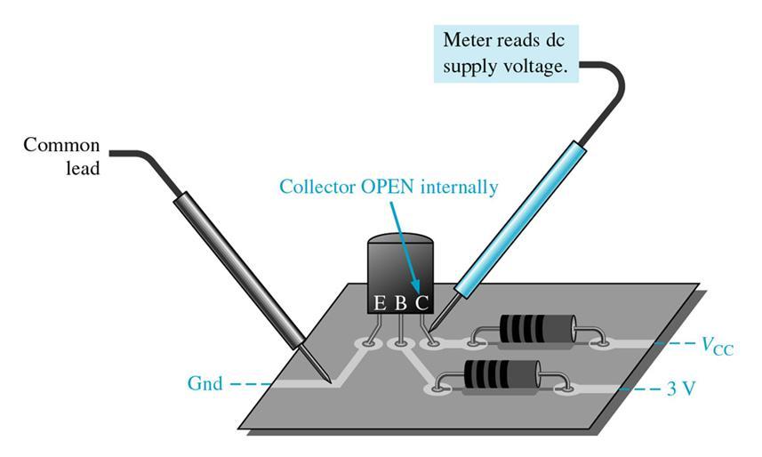
16 Objectives: Chapter 3 Section 3.9 Troubleshooting Troubleshoot various faults in transistor circuits 1. Define floating point 2. Use voltage measurements to identify a fault in a transistor circuit 3. Use a DMM to test a transistor 4. Explain how a transistor can be viewed in terms of a diode equivalent 5. Discuss in-circuit and out-of-circuit testing 6. Discuss point-of-measurement in troubleshooting 7. Discuss leakage and gain measurements


17 Troubleshooting Troubleshooting a Biased Transistor Common Faults: 1. Open bias resistors 2. Open or resistive connections 3. Shorted connections 4. Opens or shorts internal to the transistor itself Floating point refers to a point in the circuit that is not electrically connected to ground or a solid voltage
18 Troubleshooting Troubleshooting a Biased Transistor
19 Troubleshooting Troubleshooting a Biased Transistor


20 Troubleshooting Testing a Transistor with a DMM: 1. A good digital multimeter can be used as a fast and simple way to check a transistor for open or shorted junctions. 2. Recall that a good diode will show extremely high resistance with a reverse bias and a very low resistance with a forward bias. 3. Many DMMs have a diode test position that can be used. 4. DMMs without this feature, can use the ohms scale to check the resistance.

21 Troubleshooting Transistor Testers: 1. Transistor checkers will perform a comprehensive and/or automatic test(s) of the transistor curves.
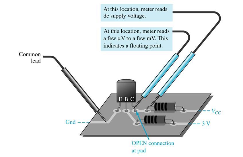
22 Troubleshooting Point-of-Measurement in Troubleshooting:

23 Troubleshooting EXAMPLE: Point-of-Measurement in Troubleshooting: 1. The transistor is in cutoff as indicated by the 10 V on the collector leads. 2. The base bias voltage of 3 V appears on the PC board but not on the transistor lead as indicated by the floating point measurement. This shows that there is an open external to the transistor between the two measured base points. 3. Check the solder joint on the base lead.


24 Troubleshooting Leakage and Gain Measurements 1. Leakage normally can be ignored 2. A faulty transistor may have more than na currents 3. Use a transistor tester 4. Gain can be determined by the transistor tester and should match the manufactures β DC 5. Most testers provide an in-circuit β DC test so that the transistor need not be removed form the circuit.
ET215 Devices I Unit 4A
 ITT Technical Institute ET215 Devices I Unit 4A Chapter 3, Section 3.1-3.2 This unit is divided into two parts; Unit 4A and Unit 4B Chapter 3 Section 3.1 Structure of Bipolar Junction Transistors The basic
EXPERIMENT 5 CURRENT AND VOLTAGE CHARACTERISTICS OF BJT
 EXPERIMENT 5 CURRENT AND VOLTAGE CHARACTERISTICS OF BJT 1. OBJECTIVES 1.1 To practice how to test NPN and PNP transistors using multimeter. 1.2 To demonstrate the relationship between collector current
The collector terminal is common to the input and output signals and is connected to the dc power supply. Common Collector Circuit
 Common Collector Circuit When you have completed this exercise, you will be able to determine the dc operating conditions of a common collector (CC) transistor circuit by using a typical CC circuit. You
ชาว ศวกรรมคอมพ วเตอร คณะว ศวกรรมศาสตร มหาว ทยาล ยเทคโนโลย ราชมงคลพระนคร
 EN2042102 วงจรไฟฟ าและอ เล กทรอน กส Circuits and Electronics บทท 7 ทรานซ สเตอร Bipolar Junction Transistor สาขาว ชาว ศวกรรมคอมพ วเตอร คณะว ศวกรรมศาสตร มหาว ทยาล ยเทคโนโลย ราชมงคลพระนคร Objectives Describe
Lecture (09) Bipolar Junction Transistor 3
 Bipolar Junction Transistor 3") Lecture (09) Bipolar Junction Transistor 3 By: Dr. Ahmed ElShafee ١ I THE BJT AS AN AMPLIFIER Amplification is the process of linearly increasing the amplitude of an electrical signal and is one of the
Lecture (09) Bipolar Junction Transistor 3 By: Dr. Ahmed ElShafee ١ I THE BJT AS AN AMPLIFIER Amplification is the process of linearly increasing the amplitude of an electrical signal and is one of the
When you have completed this exercise, you will be able to determine the ac operating characteristics of
 When you have completed this exercise, you will be able to determine the ac operating characteristics of multimeter and an oscilloscope. A sine wave generator connected between the transistor and ground
Chapter 3: Bipolar Junction Transistors
 Chapter 3: Bipolar Junction Transistors Transistor Construction There are two types of transistors: pnp npn pnp The terminals are labeled: E - Emitter B - Base C - Collector npn 2 Transistor Operation
Bipolar Junction Transistor (BJT)
") Bipolar Junction Transistor (BJT) 1 Objectives To understand the structure of BJT. To explain and analyze the basic transistor circuits. To use transistors as an amplifier and electronic switch. To design
Bipolar Junction Transistor (BJT) 1 Objectives To understand the structure of BJT. To explain and analyze the basic transistor circuits. To use transistors as an amplifier and electronic switch. To design
Electronic Devices. Floyd. Chapter 7. Ninth Edition. Electronic Devices, 9th edition Thomas L. Floyd
 Electronic Devices Ninth Edition Floyd Chapter 7 Power Amplifiers A power amplifier is a large signal amplifier that produces a replica of the input signal on its output. In the case shown here, the output
Analog Electronics. Electronic Devices, 9th edition Thomas L. Floyd Pearson Education. Upper Saddle River, NJ, All rights reserved.
 Analog Electronics BJT Structure The BJT has three regions called the emitter, base, and collector. Between the regions are junctions as indicated. The base is a thin lightly doped region compared to the
DISCUSSION The best way to test a transistor is to connect it in a circuit that uses the transistor.
 Exercise 1: EXERCISE OBJECTIVE When you have completed this exercise, you will be able to test a transistor by forward biasing and reverse biasing the junctions. You will verify your results with an ohmmeter.
Concepts to be Covered
 Introductory Medical Device Prototyping Analog Circuits Part 2 Semiconductors, http://saliterman.umn.edu/ Department of Biomedical Engineering, University of Minnesota Concepts to be Covered Semiconductors
Chapter 3. Bipolar Junction Transistors
 Chapter 3. Bipolar Junction Transistors Outline: Fundamental of Transistor Common-Base Configuration Common-Emitter Configuration Common-Collector Configuration Introduction The transistor is a three-layer
Transistor Biasing and Operational amplifier fundamentals. OP-amp Fundamentals and its DC characteristics. BJT biasing schemes
 Lab 1 Transistor Biasing and Operational amplifier fundamentals Experiment 1.1 Experiment 1.2 BJT biasing OP-amp Fundamentals and its DC characteristics BJT biasing schemes 1.1 Objective 1. To sketch potential
DC Bias. Graphical Analysis. Script
 Course: B.Sc. Applied Physical Science (Computer Science) Year & Sem.: Ist Year, Sem - IInd Subject: Electronics Paper No.: V Paper Title: Analog Circuits Lecture No.: 3 Lecture Title: Analog Circuits
Chapter 3-2 Semiconductor devices Transistors and Amplifiers-BJT Department of Mechanical Engineering
 MEMS1082 Chapter 3-2 Semiconductor devices Transistors and Amplifiers-BJT Bipolar Transistor Construction npn BJT Transistor Structure npn BJT I = I + E C I B V V BE CE = V = V B C V V E E Base-to-emitter
Tutorial 2 BJTs, Transistor Bias Circuits, BJT Amplifiers FETs and FETs Amplifiers. Part 1: BJTs, Transistor Bias Circuits and BJT Amplifiers
 Tutorial 2 BJTs, Transistor Bias Circuits, BJT Amplifiers FETs and FETs Amplifiers Part 1: BJTs, Transistor Bias Circuits and BJT Amplifiers 1. Explain the purpose of a thin, lightly doped base region.
Figure1: Basic BJT construction.
 Chapter 4: Bipolar Junction Transistors (BJTs) Bipolar Junction Transistor (BJT) Structure The BJT is constructed with three doped semiconductor regions separated by two pn junctions, as in Figure 1(a).
Bipolar Junction Transistors (BJTs)
") C H A P T E R 6 Bipolar Junction Transistors (BJTs) Figure 6.1 A simplified structure of the npn transistor and pnp transistor. Table 6.1: BJT modes of Operation Mode Cutoff Active Saturation EBJ Reverse
C H A P T E R 6 Bipolar Junction Transistors (BJTs) Figure 6.1 A simplified structure of the npn transistor and pnp transistor. Table 6.1: BJT modes of Operation Mode Cutoff Active Saturation EBJ Reverse
Transistors and Applications
 Chapter 17 Transistors and Applications DC Operation of Bipolar Junction Transistors (BJTs) The bipolar junction transistor (BJT) is constructed with three doped semiconductor regions separated by two
The first transistor. (Courtesy Bell Telephone Laboratories.)
") Fig. 3.1 The first transistor. (Courtesy Bell Telephone Laboratories.) Fig. 3.2 Types of transistors: (a) pnp; (b) npn. : (a) pnp; : (b) npn Fig. 3.3 Forward-biased junction of a pnp transistor. Fig. 3.4
Fig. 3.1 The first transistor. (Courtesy Bell Telephone Laboratories.) Fig. 3.2 Types of transistors: (a) pnp; (b) npn. : (a) pnp; : (b) npn Fig. 3.3 Forward-biased junction of a pnp transistor. Fig. 3.4
4 Transistors. 4.1 IV Relations
 4 Transistors Due date: Sunday, September 19 (midnight) Reading (Bipolar transistors): HH sections 2.01-2.07, (pgs. 62 77) Reading (Field effect transistors) : HH sections 3.01-3.03, 3.11-3.12 (pgs. 113
Chapter 5 Transistor Bias Circuits
 Chapter 5 Transistor Bias Circuits Objectives Discuss the concept of dc biasing of a transistor for linear operation Analyze voltage-divider bias, base bias, and collector-feedback bias circuits. Basic
BIPOLAR JUNCTION TRANSISTOR (BJT) NOISE MEASUREMENTS 1
 NOISE MEASUREMENTS 1") 4. BIPOLAR JUNCTION TRANSISTOR (BJT) NOISE MEASUREMENTS 4.1 Object The objective of this experiment is to measure the mean-square equivalent input noise, v 2 ni, and base spreading resistance, r x, of
4. BIPOLAR JUNCTION TRANSISTOR (BJT) NOISE MEASUREMENTS 4.1 Object The objective of this experiment is to measure the mean-square equivalent input noise, v 2 ni, and base spreading resistance, r x, of
Electronic Troubleshooting
 Electronic Troubleshooting Chapter 3 Bipolar Transistors Most devices still require some individual (discrete) transistors Used to customize operations Interface to external devices Understanding their
Chapter 6 DIFFERENT TYPES OF LOGIC GATES
 Chapter 6 DIFFERENT TYPES OF LOGIC GATES Lesson 3 RTL and DTL Gates Ch06L3-"Digital Principles and Design", Raj Kamal, Pearson Education, 2006 2 Outline Resistor transistor logic (RTL) RTL Circuit Characteristics
CHAPTER 3: BIPOLAR JUNCION TRANSISTOR DR. PHẠM NGUYỄN THANH LOAN
 CHAPTER 3: BIPOLAR JUNCION TRANSISTOR DR. PHẠM NGUYỄN THANH LOAN Hanoi, 9/24/2012 Contents 2 Structure and operation of BJT Different configurations of BJT Characteristic curves DC biasing method and analysis
Chapter 4 DC Biasing BJTs. BJTs
 hapter 4 D Biasing BJTs BJTs Biasing Biasing: The D voltages applied to a transistor in order to turn it on so that it can amplify the A signal. Operating Point The D input establishes an operating or
ECE 334: Electronic Circuits Lecture 2: BJT Large Signal Model
 Faculty of Engineering ECE 334: Electronic Circuits Lecture 2: BJT Large Signal Model Agenda I & V Notations BJT Devices & Symbols BJT Large Signal Model 2 I, V Notations (1) It is critical to understand
C H A P T E R 6 Bipolar Junction Transistors (BJTs)
") C H A P T E R 6 Bipolar Junction Transistors (BJTs) Figure 6.1 A simplified structure of the npn transistor and pnp transistor. Table 6.1: BJT modes of Operation Mode EBJ CBJ Cutoff Reverse Reverse Active
C H A P T E R 6 Bipolar Junction Transistors (BJTs) Figure 6.1 A simplified structure of the npn transistor and pnp transistor. Table 6.1: BJT modes of Operation Mode EBJ CBJ Cutoff Reverse Reverse Active
b b Fig. 1 Transistor symbols
 TRANSISTORS Transistors have three terminals which are referred to as emitter (e), base (b) and collector (c). Fig 1 shows the symbols used for the two types of transistors in common use. c c b b e e npn
Chapter 3 Bipolar Junction Transistors (BJT)
") Chapter 3 Bipolar Junction Transistors (BJT) Transistors In analog circuits, transistors are used in amplifiers and linear regulated power supplies. In digital circuits they function as electrical switches,
Chapter 3 Bipolar Junction Transistors (BJT) Transistors In analog circuits, transistors are used in amplifiers and linear regulated power supplies. In digital circuits they function as electrical switches,
Physics of Bipolar Transistor
 Physics of Bipolar Transistor Motivations - In many electronic applications, amplifier is the most fundamental building block. Ex Audio amplifier: amplifies electric signal to drive a speaker RF Power
Electronics EECE2412 Spring 2017 Exam #2
 Electronics EECE2412 Spring 2017 Exam #2 Prof. Charles A. DiMarzio Department of Electrical and Computer Engineering Northeastern University 30 March 2017 File:12198/exams/exam2 Name: : General Rules:
Transistor Configuration
 Transistor Configuration 1 Objectives To review BJT biasing circuit. To study BJT amplifier circuit To understand the BJT configuration. To analyse single-stage BJT amplifier circuits. To study the differential
ELEC 2210 EXPERIMENT 7 The Bipolar Junction Transistor (BJT)
") ELEC 2210 EXPERIMENT 7 The Bipolar Junction Transistor (BJT) Objectives: The experiments in this laboratory exercise will provide an introduction to the BJT. You will use the Bit Bucket breadboarding system
ELEC 2210 EXPERIMENT 7 The Bipolar Junction Transistor (BJT) Objectives: The experiments in this laboratory exercise will provide an introduction to the BJT. You will use the Bit Bucket breadboarding system
Chapter 3: TRANSISTORS. Dr. Gopika Sood PG Govt. College For Girls Sector -11, Chandigarh
 Chapter 3: TRANSISTORS Dr. Gopika Sood PG Govt. College For Girls Sector -11, Chandigarh OUTLINE Transistors Bipolar Junction Transistor (BJT) Operation of Transistor Transistor parameters Load Line Biasing
Electronic Circuits. Power Amplifiers. Manar Mohaisen Office: F208 Department of EECE
 Electronic Circuits Power Amplifiers Manar Mohaisen Office: F208 Email: manar.subhi@kut.ac.kr Department of EECE Review of the Precedent Lecture Explain the Amplifier Operation Explain the BJT AC Models
Lecture 3: Transistors
 Lecture 3: Transistors Now that we know about diodes, let s put two of them together, as follows: collector base emitter n p n moderately doped lightly doped, and very thin heavily doped At first glance,
STATIC CHARACTERISTICS OF TRANSISTOR
 STAT CHARACTERISTS OF TRANSISTOR OBJECTIVE The purpose of the experiment is to study the characteristics of bipolar transistor in common emitter (CE) configuration. From the characteristic curve it is
การไบอ สทรานซ สเตอร. Transistors Biasing
 การไบอ สทรานซ สเตอร Transistors iasing iasing iasing: Applying D voltages to a transistor in order to turn it on so that it can amplify A signals. The D input establishes an operating or quiescent point
(a) BJT-OPERATING MODES & CONFIGURATIONS
 BJT-OPERATING MODES & CONFIGURATIONS") (a) BJT-OPERATING MODES & CONFIGURATIONS 1. The leakage current I CBO flows in (a) The emitter, base and collector leads (b) The emitter and base leads. (c) The emitter and collector leads. (d) The base
(a) BJT-OPERATING MODES & CONFIGURATIONS 1. The leakage current I CBO flows in (a) The emitter, base and collector leads (b) The emitter and base leads. (c) The emitter and collector leads. (d) The base
ECE321 Electronics I Fall 2006
 ECE321 Electronics I Fall 2006 Professor James E. Morris Lecture 11 31 st October, 2006 Bipolar Junction Transistors (BJTs) 5.1 Device Structure & Physics 5.2 I-V Characteristics Convert 5.1 information
o Semiconductor Diode Symbol: The cathode contains the N-type material and the anode contains the P-type material.
 Cornerstone Electronics Technology and Robotics I Week 16 Diodes and Transistor Switches Administration: o Prayer o Turn in quiz Review: o Design and wire a voltage divider that divides your +9 V voltage
Lecture #3 BJT Transistors & DC Biasing
 November 2014 Ahmad El-Banna Integrated Technical Education Cluster At AlAmeeria J-601-1448 Electronic Principals Lecture #3 BJT Transistors & DC Biasing Instructor: Dr. Ahmad El-Banna Agenda Transistor
Exercise 2: Collector Current Versus Base Current
 Exercise 2: Collector Current Versus Base Current EXERCISE OBJECTIVE When you have completed this exercise, you will be able to demonstrate the relationship of collector current to base current by using
Experiment 9 Bipolar Junction Transistor Characteristics
 Experiment 9 Bipolar Junction Transistor Characteristics W.T. Yeung, W.Y. Leung, and R.T. Howe UC Berkeley EE 105 Fall 2005 1.0 Objective In this lab, you will determine the I C - V CE characteristics
Electronic Circuits II Laboratory 01 Voltage Divider Bias
 Electronic Circuits II Laboratory 01 Voltage Divider Bias # Student ID Student Name Grade (10) 1 Instructor signature 2 3 4 5 Delivery Date -1 / 8 - Objective The objective of this exercise is to examine
Analog Circuits Part 2 Semiconductors
 Introductory Medical Device Prototyping Analog Circuits Part 2 Semiconductors, http://saliterman.umn.edu/ Department of Biomedical Engineering, University of Minnesota Concepts to be Covered Semiconductors
Features: Phase A Phase B Phase C -DC_A -DC_B -DC_C
 Three Phase Inverter Power Stage Description: The SixPac TM from Applied Power Systems is a configurable IGBT based power stage that is configured as a three-phase bridge inverter for motor control, power
.dc Vcc Ib 0 50uA 5uA
 EE 2274 BJT Biasing PreLab: 1. Common Emitter (CE) Transistor Characteristics curve Generate the characteristics curves for a 2N3904 in LTspice by plotting Ic by sweeping Vce over a set of Ib steps. Label
University of Southern C alifornia School Of Engineering Department Of Electrical Engineering
 University of Southern C alifornia School Of Engineering Department Of Electrical Engineering EE 348: Homework Assignment #04 Spring, 2001 (Due 02/27/2001) Choma Problem #16: n monolithic circuits, diodes
EXPERIMENT 6 REPORT Bipolar Junction Transistor (BJT) Characteristics
 Characteristics") Name & Surname: ID: Date: EXPERIMENT 6 REPORT Bipolar Junction Transistor (BJT) Characteristics Objectives: 1. To determine transistor type (npn, pnp),terminals, and material using a DMM 2. To graph the
Name & Surname: ID: Date: EXPERIMENT 6 REPORT Bipolar Junction Transistor (BJT) Characteristics Objectives: 1. To determine transistor type (npn, pnp),terminals, and material using a DMM 2. To graph the
LABORATORY MODULE. Analog Electronics. Semester 2 (2005/2006)
") LABORATORY MODULE ENT 162 Analog Electronics Semester 2 (2005/2006) EXPERIMENT 5 : The Class A Common-Emitter Power Amplifier Name Matrix No. : : PUSAT PENGAJIAN KEJURUTERAAN MEKATRONIK KOLEJ UNIVERSITI
LABORATORY MODULE ENT 162 Analog Electronics Semester 2 (2005/2006) EXPERIMENT 5 : The Class A Common-Emitter Power Amplifier Name Matrix No. : : PUSAT PENGAJIAN KEJURUTERAAN MEKATRONIK KOLEJ UNIVERSITI
Electronics Fundamentals BIPOLAR TRANSISTORS. Construction, circuit symbols and biasing examples for NPN and PNP junction transistors.
 IPOLA TANSISTOS onstruction, circuit symbols and biasing examples for NPN and PNP junction transistors Slide 1 xternal bias voltages create an electric field, which pulls electrons (emitted into the base
Lab 3: BJT Digital Switch
 Lab 3: BJT Digital Switch Objectives The purpose of this lab is to acquaint you with the basic operation of bipolar junction transistor (BJT) and to demonstrate its functionality in digital switching circuits.
4.1.3 Structure of Actual Transistors
 4.1.3 Structure of Actual Transistors Figure 4.7 shows a more realistic BJT cross-section Collector virtually surrounds entire emitter region This makes it difficult for electrons injected into base to
Transistor Configuration
 Transistor Configuration 1 Objectives To review BJT biasing circuit. To study BJT amplifier circuit To understand the BJT configuration. To analyse single-stage BJT amplifier circuits. To study the differential
TENTATIVE PP225D120. POW-R-PAK TM 225A / 1200V Half Bridge IGBT Assembly. Description:
 Description: The Powerex is a configurable IGBT based power assembly that may be used as a converter, chopper, half or full bridge, or three phase inverter for motor control, power supply, UPS or other
BJT. Bipolar Junction Transistor BJT BJT 11/6/2018. Dr. Satish Chandra, Assistant Professor, P P N College, Kanpur 1
 BJT Bipolar Junction Transistor Satish Chandra Assistant Professor Department of Physics P P N College, Kanpur www.satish0402.weebly.com The Bipolar Junction Transistor is a semiconductor device which
BJT Characteristics & Common Emitter Transistor Amplifier
 LAB #07 Objectives 1. To graph the collector characteristics of a transistor. 2. To measure AC and DC voltages in a common-emitter amplifier. Theory BJT A bipolar (junction) transistor (BJT) is a three-terminal
Transistor fundamentals Nafees Ahamad
 Transistor fundamentals Nafees Ahamad Asstt. Prof., EECE Deptt, DIT University, Dehradun Website: www.eedofdit.weebly.com Transistor A transistor consists of two PN junctions formed by sandwiching either
Introduction PNP C NPN C
 Introduction JT Transistors: A JT (or any transistor) can be used either as a switch with positions of on or off, or an amplifier that controls its output at all levels in between the extreme on or off
Lecture (08) Bipolar Junction Transistor (2)
 Bipolar Junction Transistor (2)") Lecture (08) ipolar Junction Transistor (2) y: Dr. Ahmed lshafee 1 JT haracteristic ollector haracteristic urves 2 Applying fixed V, increasing V Saturation Assume that V is set to produce a certain value
Lecture (08) ipolar Junction Transistor (2) y: Dr. Ahmed lshafee 1 JT haracteristic ollector haracteristic urves 2 Applying fixed V, increasing V Saturation Assume that V is set to produce a certain value
Transistor Biasing Nafees Ahamad
 Transistor Biasing Nafees Ahamad Asstt. Prof., EECE Deptt, DIT University, Dehradun Website: www.eedofdit.weebly.com Introduction The basic function of transistor is to do amplification. (CE connection)
Bipolar Junction Transistors
 Bipolar Junction Transistors Invented in 1948 at Bell Telephone laboratories Bipolar junction transistor (BJT) - one of the major three terminal devices Three terminal devices more useful than two terminal
EE105 Fall 2014 Microelectronic Devices and Circuits. NPN Bipolar Junction Transistor (BJT)
") EE105 Fall 2014 Microelectronic Devices and Circuits Prof. Ming C. Wu wu@eecs.berkeley.edu 511 utardja Dai Hall (DH) 1 NPN Bipolar Junction Transistor (BJT) Forward Bias Reverse Bias Hole Flow Electron
EE105 Fall 2014 Microelectronic Devices and Circuits Prof. Ming C. Wu wu@eecs.berkeley.edu 511 utardja Dai Hall (DH) 1 NPN Bipolar Junction Transistor (BJT) Forward Bias Reverse Bias Hole Flow Electron
TO-92 SOT-23 Mark: 3B. TA = 25 C unless otherwise noted. Symbol Parameter Value Units
 PN98 Discrete POWER & Signal Technologies MMBT98 C C B E TO-92 SOT-23 Mark: 3B B E This device is designed for use as RF amplifiers, oscillators and multipliers with collector currents in the.0 ma to 30
Advanced Monolithic Systems
 Advanced Monolithic Systems FEATURES Internal Power Switch Output Voltage up to 20V Up to 89% Efficiency Low 0.08µA Shutdown Supply Current Internal Current Limit Thermal Shutdown Available in 5-Pin SOT-23
Transistor Biasing. DC Biasing of BJT. Transistor Biasing. Transistor Biasing 11/23/2018
 Transistor Biasing DC Biasing of BJT Satish Chandra Assistant Professor Department of Physics P P N College, Kanpur www.satish0402.weebly.com A transistors steady state of operation depends a great deal
Lecture 12. Bipolar Junction Transistor (BJT) BJT 1-1
 BJT 1-1") Lecture 12 Bipolar Junction Transistor (BJT) BJT 1-1 Course Info Lecture hours: 4 Two Lectures weekly (Saturdays and Wednesdays) Location: K2 Time: 1:40 pm Tutorial hours: 2 One tutorial class every week
Lecture 12 Bipolar Junction Transistor (BJT) BJT 1-1 Course Info Lecture hours: 4 Two Lectures weekly (Saturdays and Wednesdays) Location: K2 Time: 1:40 pm Tutorial hours: 2 One tutorial class every week
Lecture (06) Bipolar Junction Transistor
 Bipolar Junction Transistor") Lecture (06) Bipolar Junction Transistor By: Dr. Ahmed lshafee ١ Agenda BJT structure BJT operation BJT characteristics ٢ BJT structure The BJT is constructed with three doped semiconductor regions One
Lecture (06) Bipolar Junction Transistor By: Dr. Ahmed lshafee ١ Agenda BJT structure BJT operation BJT characteristics ٢ BJT structure The BJT is constructed with three doped semiconductor regions One
Electronics II Lecture 2(a): Bipolar Junction Transistors
: Bipolar Junction Transistors") Lecture 2(a): Bipolar Junction Transistors A/Lectr. Khalid Shakir Dept. Of Engineering Engineering by Pearson Transistor! Transistor=Transfer+Resistor. When Transistor operates in active region its input
Lecture 2(a): Bipolar Junction Transistors A/Lectr. Khalid Shakir Dept. Of Engineering Engineering by Pearson Transistor! Transistor=Transfer+Resistor. When Transistor operates in active region its input
I C I E =I B = I C 1 V BE 0.7 V
 Guide to NPN Amplifier Analysis Jason Woytowich 1. Transistor characteristics A BJT has three operating modes cutoff, active, and saturation. For applications, like amplifiers, where linear characteristics
Practical 2P12 Semiconductor Devices
 Practical 2P12 Semiconductor Devices What you should learn from this practical Science This practical illustrates some points from the lecture courses on Semiconductor Materials and Semiconductor Devices
Shown here is a schematic diagram for a real inverter circuit, complete with all necessary components for efficient and reliable operation:
 The NOT gate The single-transistor inverter circuit illustrated earlier is actually too crude to be of practical use as a gate. Real inverter circuits contain more than one transistor to maximize voltage
By: Dr. Ahmed ElShafee
 Lecture (02) Transistor operating point & DC Load line (2), Transistor Bias Circuit 1 By: Dr. Ahmed ElShafee ١ DC Load Line The dc operation can be described graphically using a dc load line. This is a
MAHARASHTRA STATE BOARD OF TECHNICAL EDUCATION (Autonomous) (ISO/IEC Certified) MODEL ANSWER
 (ISO/IEC Certified) MODEL ANSWER") Important Instructions to examiners: 1) The answers should be examined by key words and not as word-to-word as given in the model answer scheme. 2) The model answer and the answer written by candidate
Important Instructions to examiners: 1) The answers should be examined by key words and not as word-to-word as given in the model answer scheme. 2) The model answer and the answer written by candidate
Structure of Actual Transistors
 4.1.3. Structure of Actual Transistors Figure 4.7 shows a more realistic BJT cross-section Collector virtually surrounds entire emitter region This makes it difficult for electrons injected into base to
PHY405F 2009 EXPERIMENT 6 SIMPLE TRANSISTOR CIRCUITS
 PHY405F 2009 EXPERIMENT 6 SIMPLE TRANSISTOR CIRCUITS Due Date (NOTE CHANGE): Thursday, Nov 12 th @ 5 pm; Late penalty in effect! Most active electronic devices are based on the transistor as the fundamental
EE105 Fall 2015 Microelectronic Devices and Circuits
 EE105 Fall 2015 Microelectronic Devices and Circuits Prof. Ming C. Wu wu@eecs.berkeley.edu 511 Sutardja Dai Hall (SDH) 11-1 Transistor Operating Mode in Amplifiers Transistors are biased in flat part of
HOME ASSIGNMENT. Figure.Q3
 HOME ASSIGNMENT 1. For the differential amplifier circuit shown below in figure.q1, let I=1 ma, V CC =5V, v CM = -2V, R C =3kΩ and β=100. Assume that the BJTs have v BE =0.7 V at i C =1 ma. Find the voltage
The shape of the waveform will be the same, but its level is shifted either upward or downward. The values of the resistor R and capacitor C affect
 Diode as Clamper A clamping circuit is used to place either the positive or negative peak of a signal at a desired level. The dc component is simply added or subtracted to/from the input signal. The clamper
PHYS 3152 Methods of Experimental Physics I E2. Diodes and Transistors 1
 Part I Diodes Purpose PHYS 3152 Methods of Experimental Physics I E2. In this experiment, you will investigate the current-voltage characteristic of a semiconductor diode and examine the applications of
Chapter 6: Transistors and Gain
 I. Introduction Chapter 6: Transistors and Gain This week we introduce the transistor. Transistors are three-terminal devices that can amplify a signal and increase the signal s power. The price is that
The Common Emitter Amplifier Circuit
 The Common Emitter Amplifier Circuit In the Bipolar Transistor tutorial, we saw that the most common circuit configuration for an NPN transistor is that of the Common Emitter Amplifier circuit and that
UNIT-III Bipolar Junction Transistor
 DC UNT-3.xplain the construction and working of JT. UNT- ipolar Junction Transistor A bipolar (junction) transistor (JT) is a three-terminal electronic device constructed of doped semiconductor material
Phy 335, Unit 4 Transistors and transistor circuits (part one)
") Mini-lecture topics (multiple lectures): Phy 335, Unit 4 Transistors and transistor circuits (part one) p-n junctions re-visited How does a bipolar transistor works; analogy with a valve Basic circuit
Mini-lecture topics (multiple lectures): Phy 335, Unit 4 Transistors and transistor circuits (part one) p-n junctions re-visited How does a bipolar transistor works; analogy with a valve Basic circuit
SCHEMATIC OF GRAYMARK 808 POWERED BREADBOARD
 SCHEMATIC OF GRAYMARK 808 POWERED BREADBOARD 1a white SW1 white 2a TP1 blue TP2 black blue TP3 TP4 yellow TP5 yellow TP6 4 3 8 7 + D1 D2 D5 D6 C1 R1 TP8 Q1 R3 TP12 2 TP18 U2-0-15V C8 9 C2 + TP15 C5 R12
Lab 2: Discrete BJT Op-Amps (Part I)
") Lab 2: Discrete BJT Op-Amps (Part I) This is a three-week laboratory. You are required to write only one lab report for all parts of this experiment. 1.0. INTRODUCTION In this lab, we will introduce and
Lab 2: Discrete BJT Op-Amps (Part I) This is a three-week laboratory. You are required to write only one lab report for all parts of this experiment. 1.0. INTRODUCTION In this lab, we will introduce and
Technical. Application. Assembly. Availability. Pricing. Phone
 6121 Baker Road, Suite 108 Minnetonka, MN 55345 www.chtechnology.com Phone (952) 933-6190 Fax (952) 933-6223 1-800-274-4284 Thank you for downloading this document from C&H Technology, Inc. Please contact
E C B E. TO-92 SOT-23 Mark: 2X. TA = 25 C unless otherwise noted. Symbol Parameter Value Units
 2N4401 MMBT4401 C 2N4401 / MMBT4401 E C B E TO-92 SOT-23 Mark: 2X B NPN General Pupose Amplifier This device is designed for use as a medium power amplifier and switch requiring collector currents up to
PHYS225 Lecture 6. Electronic Circuits
 PHYS225 Lecture 6 Electronic Circuits Transistors History Basic physics of operation Ebers-Moll model Small signal equivalent Last lecture Introduction to Transistors A transistor is a device with three
Experiment #8: Designing and Measuring a Common-Collector Amplifier
 SCHOOL OF ENGINEERING AND APPLIED SCIENCE DEPARTMENT OF ELECTRICAL AND COMPUTER ENGINEERING ECE 2115: ENGINEERING ELECTRONICS LABORATORY Experiment #8: Designing and Measuring a Common-Collector Amplifier
Electronics 1 Lab (CME 2410)
") Electronics 1 Lab (CME 2410) School of Informatics & Computing German Jordanian University Laboratory Experiment (7) 1. Objective: The Bipolar Junction Transistor (BJT) DC Bias Stabilization 1. To be familiar
Electronics 1 Lab (CME 2410) School of Informatics & Computing German Jordanian University Laboratory Experiment (7) 1. Objective: The Bipolar Junction Transistor (BJT) DC Bias Stabilization 1. To be familiar
Electronic Circuits ELCT604 (Spring 2018) Lecture 2 BJT Amplifiers
 Lecture 2 BJT Amplifiers") Electronic Circuits ELCT604 (Spring 2018) Lecture 2 BJT Amplifiers Assistant Professor Office: C3.315 E-mail: eman.azab@guc.edu.eg 1 Analog Voltage Amplifiers Circuit Design and Configurations 2 Objective
Electronic Circuits ELCT604 (Spring 2018) Lecture 2 BJT Amplifiers Assistant Professor Office: C3.315 E-mail: eman.azab@guc.edu.eg 1 Analog Voltage Amplifiers Circuit Design and Configurations 2 Objective
Transistor Characteristics
 Transistor Characteristics Topics covered in this presentation: Transistor Construction Transistor Operation Transistor Characteristics 1 of 15 The Transistor The transistor is a semiconductor device that
Dual Bias Resistor Transistors
 DATA SHEET SEMICONDUCTOR MUN5DW Series Dual Bias Resistor Transistors PNP Silicon Surface Mount Transistors with Monolithic Bias Resistor Network The BRT (Bias Resistor Transistor) contains a single transistor
10 Semiconductors - Transistors
 10 Semiconductors - Transistors The transistor was invented in the late 1940s. Credit for its invention is given to three Bell Laboratories scientists, John Bardeen, Walter Brattain, and William Shockley.
ESE 372 / Spring 2011 / Lecture 19 Common Base Biased by current source
 ESE 372 / Spring 2011 / Lecture 19 Common Base Biased by current source Output from Collector Start with bias DC analysis make sure BJT is in FA, then calculate small signal parameters for AC analysis.