Lecture (05) BJT Amplifiers 2
|
|
|
- Abel Whitehead
- 5 years ago
- Views:
Transcription
1 Lecture (05) BJT Amplifiers 2 By: Dr. Ahmed ElShafee 1 Effect of the Emitter Bypass Capacitor on Voltage Gain The emitter bypass capacitor, provides an effective short to the ac signal around the emitter resistor, thus keeping the emitter at ac ground. With the bypass capacitor, the gain of a given amplifier is maximum. 2
2 The value of the bypass capacitor must be large enough so that its reactance over the frequency range of the amplifier is very small (ideally ) compared to RE. A good rule of thumb is that the capacitive reactance, XC, of the bypass capacitor should be at least 10 times smaller than RE at the minimum frequency for which the amplifier must operate 3 Example 01 Select a minimum value for the emitter bypass capacitor, C2, in Figure if the amplifier must operate over a frequency range from 200 Hz to 10 khz. 4


3 5 Voltage Gain Without the Bypass Capacitor To see how the bypass capacitor affects ac voltage gain, let s remove it from the circuit in, compare voltage gains. Without the bypass capacitor, the emitter is no longer at ac ground. Instead, RE is seen by the ac signal between the emitter and ground and effectively adds to in the voltage gain formula. 6


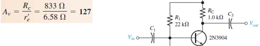
4 Example 02 Calculate the base to collector voltage gain of the amplifier in Figure both without and with an emitter bypass capacitor if there is no load resistor 7 8


5 Effect of a Load on the Voltage Gain A load is the amount of current drawn from the output of an amplifier or other circuit through a load resistance 9 The total ac collector resistance is Replacing RC with Rc in the voltage gain expression gives When Rc<<RC, because of RL, the voltage gain is reduced. However, if RL>>RC then Rc == RC and the load has very little effect on the gain. 10

6 Example

7 Stability of the Voltage Gain Stability is a measure of how well an amplifier maintains its design values over changes in temperature or for a transistor with a different β As Av = RC/r e r e depends on IE and temp with RE unbypassed, the gain is much less dependent on r e as, but gain is reduced too 13 Swamping r e to Stabilize the Voltage Gain Swamping is a method used to minimize the effect of without reducing the voltage gain to its minimum value. In a swamped amplifier, RE is partially bypassed so that a reasonable gain can be achieved, RE, is formed with two separate emitter resistors, RE1 and RE2, Both resistors (RE1 RE2) affect the dc bias while only RE1 affects the ac voltage gain 14

8 If RE1 is at least ten times larger than r e approximate voltage gain for the swamped amplifier is 15 Example 02 16
9 17 The Effect of Swamping on the Amplifier s Input Resistance looking in at the base of a common emitter amplifier with RE completely bypassed, is When the emitter resistance is partially bypassed, the portion of the resistance that is unbypassed is seen by the ac signal and results in an increase in the ac input resistance by appearing in series with re 18

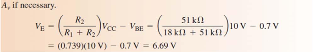
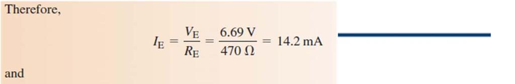
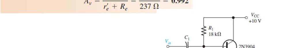
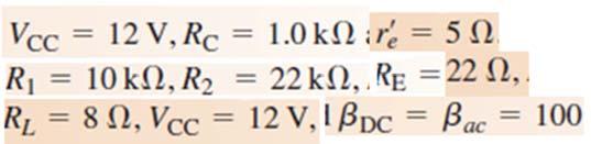
10 Example rms (a) Determine the dc collector voltage. 20


11 21 (b) Determine the ac collector voltage. 22


12 23 24


13 25 (c) Draw the total collector voltage waveform and the total output voltage waveform 26
14 27 Current Gain 28
15 Power Gain The overall power gain is the product of the overall voltage gain (Av ) and the overall current gain (Ai). 29 THE COMMON COLLECTOR AMPLIFIER An emitter follower circuit with voltage divider bias is shown in Figure, the input signal is capacitively coupled to the base, the output signal is capacitively coupled from the emitter, and the collector is at ac ground. There is no phase inversion, the output is approximately the same amplitude as the input 30

16 gain The capacitive reactances are assumed to be negligible at the frequency of operation. where Re is the parallel combination of RE and RL 31 If there is no load, then Re RE.. Since the output voltage is at the emitter, it is in phase with the base voltage, so there is no inversion from input to output. Because there is no inversion and because the voltage gain is approximately 1, the output voltage closely follows the input voltage in both phase and amplitude; thus the 32 term emitter follower.
17 Input Resistance The emitter follower is characterized by a high input resistance; this is what makes it a useful circuit. Because of the high input resistance, it can be used as a buffer to minimize loading effects when a circuit is driving a lowresistance load
18 Output Resistance 35 Current Gain 36

19 Power Gain 37 Example 01 38

20 39 40


21 41 The Darlington Pair βac is a major factor in determining the input resistance of an amplifier. One way to boost input resistance is to use a Darlington pair 42
22 Neglecting r e 43 An Application The emitter follower is often used as an interface between a circuit with a high output resistance and a low resistance load. In such an application, the emitterfollower is called a buffer. Suppose a common emitter amplifier with a collector resistance 1k ohm, must drive a low resistance load such as an 8 ohm lowpower speaker. This results in an ac collector resistance of 44


23 if the speaker is capacitively coupled to the output of the amplifier, the load appears8 ohm to the ac signal in parallel with the collector resistor. 1k 45 An emitter follower using a Darlington pair can be used to interface the amplifier and the speaker, 46
")


24 Example (a) Determine the voltage gain of the common emitter amplifier 48


 to be The")

25 49 (b) Determine the voltage gain of the Darlington emitterfollower. The effective ac emitter resistance was found in part (a) to be The voltage gain for the Darlington emitter follower is 50
26 (c) Determine the overall voltage gain and compare to the gain of the common emitter amplifier driving the speaker directly without the Darlington emitter follower. 51 The Sziklai Pair The Sziklai pair, is similar to the Darlington pair except that it consists of two types of transistors, an npn and a pnp. known as a complementary Darlington or a compound transistor The current gain is about the same as in the Darlington pair, as illustrated. The difference is that the Q2 base current is the Q1 collector current instead of emitter current, as in the Darlington arrangement. 52
27 An advantage of the Sziklai pair, compared to the Darlington, is that it takes less voltage to turn it on because only one barrier potential has to be overcome. 53 Thanks,.. See you next week (ISA), 54
Lecture (06) BJT Amplifiers 3
 BJT Amplifiers 3") Lecture (06) BJT Amplifiers 3 By: Dr. Ahmed ElShafee ١ THE COMMON COLLECTOR AMPLIFIER An emitter follower circuit with voltage divider bias is shown in Figure, the input signal is capacitively coupled
Lecture (06) BJT Amplifiers 3 By: Dr. Ahmed ElShafee ١ THE COMMON COLLECTOR AMPLIFIER An emitter follower circuit with voltage divider bias is shown in Figure, the input signal is capacitively coupled
Lecture (06) BJT Amplifiers 3
 BJT Amplifiers 3") Lecture (06) BJT Amplifiers 3 By: Dr. Ahmed ElShafee 1 Current Gain 2 Power Gain The overall power gain is the product of the overall voltage gain (Av ) and the overall current gain (Ai). 3 THE COMMON
Lecture (06) BJT Amplifiers 3 By: Dr. Ahmed ElShafee 1 Current Gain 2 Power Gain The overall power gain is the product of the overall voltage gain (Av ) and the overall current gain (Ai). 3 THE COMMON
Lecture (04) BJT Amplifiers 1
 BJT Amplifiers 1") Lecture (04) BJT Amplifiers 1 By: Dr. Ahmed ElShafee ١ The Linear Amplifier A linear amplifier provides amplification of a signal without any distortion so that the output signal A voltage divider biased
Lecture (04) BJT Amplifiers 1 By: Dr. Ahmed ElShafee ١ The Linear Amplifier A linear amplifier provides amplification of a signal without any distortion so that the output signal A voltage divider biased
By: Dr. Ahmed ElShafee
 Lecture (04) Transistor Bias Circuit 3 BJT Amplifiers 1 By: Dr. Ahmed ElShafee ١ Emitter Feedback Bias If an emitter resistor is added to the base bias circuit in Figure, the result is emitter feedback
Electronic Devices. Floyd. Chapter 6. Ninth Edition. Electronic Devices, 9th edition Thomas L. Floyd
 Electronic Devices Ninth Edition Floyd Chapter 6 Agenda BJT AC Analysis Linear Amplifier AC Load Line Transistor AC Model Common Emitter Amplifier Common Collector Amplifier Common Base Amplifier Special
Electrical, Electronic and Digital Principles (EEDP) Lecture 5. CE Amplifier, Coupling, and Multistage Amplifiers باسم ممدوح الحلوانى
 Lecture 5. CE Amplifier, Coupling, and Multistage Amplifiers باسم ممدوح الحلوانى") Electrical, Electronic and Digital Principles (EEDP) Lecture 5 CE Amplifier, Coupling, and Multistage Amplifiers د. باسم ممدوح الحلوانى Total Output Resistance The output resistance of any system is defined
Electrical, Electronic and Digital Principles (EEDP) Lecture 5 CE Amplifier, Coupling, and Multistage Amplifiers د. باسم ممدوح الحلوانى Total Output Resistance The output resistance of any system is defined
PartIIILectures. Multistage Amplifiers
 University of missan Electronic II, Second year 2015-2016 PartIIILectures Assistant Lecture: 1 Multistage and Compound Amplifiers Basic Definitions: 1- Gain of Multistage Amplifier: Fig.(1-1) A general
Lab 4. Transistor as an amplifier, part 2
 Lab 4 Transistor as an amplifier, part 2 INTRODUCTION We continue the bi-polar transistor experiments begun in the preceding experiment. In the common emitter amplifier experiment, you will learn techniques
... Second Semester
 كنا نظنك اي عيل تركتنا... لكن طيفك مل يزل يغشانا مثل الندى يسقي النبات بقطره... قد ابت ليال يف ادلىج عطشاان ما زلت أذكر حني أدخل معمال... متسك هجازا للقياس تحاكه... فأ راك جتلس هادئا حيرانا تكتب وترمس
Chapter 11 Output Stages
 1 Chapter 11 Output Stages Learning Objectives 2 1) The classification of amplifier output stages 2) Analysis and design of a variety of output-stage types 3) Overview of power amplifiers Introduction
ANALOG FUNDAMENTALS C. Topic 4 BASIC FET AMPLIFIER CONFIGURATIONS
 AV18-AFC ANALOG FUNDAMENTALS C Topic 4 BASIC FET AMPLIFIER CONFIGURATIONS 1 ANALOG FUNDAMENTALS C AV18-AFC Overview This topic identifies the basic FET amplifier configurations and their principles of
Electronic Devices. Floyd. Chapter 7. Ninth Edition. Electronic Devices, 9th edition Thomas L. Floyd
 Electronic Devices Ninth Edition Floyd Chapter 7 Power Amplifiers A power amplifier is a large signal amplifier that produces a replica of the input signal on its output. In the case shown here, the output
Experiment No. 9 DESIGN AND CHARACTERISTICS OF COMMON BASE AND COMMON COLLECTOR AMPLIFIERS
 Experiment No. 9 DESIGN AND CHARACTERISTICS OF COMMON BASE AND COMMON COLLECTOR AMPLIFIERS 1. Objective: The objective of this experiment is to explore the basic applications of the bipolar junction transistor
EXPERIMENT 12: SIMULATION STUDY OF DIFFERENT BIASING CIRCUITS USING NPN BJT
 EXPERIMENT 12: SIMULATION STUDY OF DIFFERENT BIASING CIRCUITS USING NPN BJT AIM: 1) To study different BJT DC biasing circuits 2) To design voltage divider bias circuit using NPN BJT SOFTWARE TOOL: PC
Lecture (09) Bipolar Junction Transistor 3
 Bipolar Junction Transistor 3") Lecture (09) Bipolar Junction Transistor 3 By: Dr. Ahmed ElShafee ١ I THE BJT AS AN AMPLIFIER Amplification is the process of linearly increasing the amplitude of an electrical signal and is one of the
Lecture (09) Bipolar Junction Transistor 3 By: Dr. Ahmed ElShafee ١ I THE BJT AS AN AMPLIFIER Amplification is the process of linearly increasing the amplitude of an electrical signal and is one of the
Electronics EECE2412 Spring 2017 Exam #2
 Electronics EECE2412 Spring 2017 Exam #2 Prof. Charles A. DiMarzio Department of Electrical and Computer Engineering Northeastern University 30 March 2017 File:12198/exams/exam2 Name: : General Rules:
Transistors and Applications
 Chapter 17 Transistors and Applications DC Operation of Bipolar Junction Transistors (BJTs) The bipolar junction transistor (BJT) is constructed with three doped semiconductor regions separated by two
ESE 372 / Spring 2011 / Lecture 19 Common Base Biased by current source
 ESE 372 / Spring 2011 / Lecture 19 Common Base Biased by current source Output from Collector Start with bias DC analysis make sure BJT is in FA, then calculate small signal parameters for AC analysis.
Last time: BJT CE and CB amplifiers biased by current source
 Last time: BJT CE and CB amplifiers biased by current source Assume FA regime, then VB VC V E I B I E, β 1 I Q C α I, V 0. 7V Calculate V CE and confirm it is > 0.2-0.3V, then BJT can be replaced with
The George Washington University School of Engineering and Applied Science Department of Electrical and Computer Engineering ECE 20 - LAB
 The George Washington University School of Engineering and Applied Science Department of Electrical and Computer Engineering ECE 20 - LAB Experiment # 6 (Part I) Bipolar Junction Transistors Common Emitter
Electronics Lab. (EE21338)
") Princess Sumaya University for Technology The King Abdullah II School for Engineering Electrical Engineering Department Electronics Lab. (EE21338) Prepared By: Eng. Eyad Al-Kouz October, 2012 Table of
Princess Sumaya University for Technology The King Abdullah II School for Engineering Electrical Engineering Department Electronics Lab. (EE21338) Prepared By: Eng. Eyad Al-Kouz October, 2012 Table of
THE UNIVERSITY OF HONG KONG. Department of Electrical and Electrical Engineering
 THE UNIVERSITY OF HONG KONG Department of Electrical and Electrical Engineering Experiment EC1 The Common-Emitter Amplifier Location: Part I Laboratory CYC 102 Objective: To study the basic operation and
2. SINGLE STAGE BIPOLAR JUNCTION TRANSISTOR (BJT) AMPLIFIERS
 AMPLIFIERS") 2. SINGLE STAGE BIPOLAR JUNCTION TRANSISTOR (BJT) AMPLIFIERS I. Objectives and Contents The goal of this experiment is to become familiar with BJT as an amplifier and to evaluate the basic configurations
2. SINGLE STAGE BIPOLAR JUNCTION TRANSISTOR (BJT) AMPLIFIERS I. Objectives and Contents The goal of this experiment is to become familiar with BJT as an amplifier and to evaluate the basic configurations
By: Dr. Ahmed ElShafee
 Lecture (02) Transistor operating point & DC Load line (2), Transistor Bias Circuit 1 By: Dr. Ahmed ElShafee ١ DC Load Line The dc operation can be described graphically using a dc load line. This is a
UNIVERSITY OF UTAH ELECTRICAL ENGINEERING DEPARTMENT
 UNIVERSITY OF UTAH ELECTRICAL ENGINEERING DEPARTMENT ECE 3110 LAB EXPERIMENT NO. 4 CLASS AB POWER OUTPUT STAGE Objective: In this laboratory exercise you will build and characterize a class AB power output
Lecture (10) Power Amplifiers (2)
 Power Amplifiers (2)") Lecture (10) Power Amplifiers (2) By: Dr. Ahmed ElShafee ١ Class B/AB Power the ideal maximum peak output current for both dual supply and single supply push pull amplifiers is approximately Ic(sat), and
Lecture (10) Power Amplifiers (2) By: Dr. Ahmed ElShafee ١ Class B/AB Power the ideal maximum peak output current for both dual supply and single supply push pull amplifiers is approximately Ic(sat), and
Lecture (07) BJT Amplifiers 4 JFET (1)
 BJT Amplifiers 4 JFET (1)") Lecture (07) BJT Amplifiers 4 JFET (1) By: r. Ahmed Elhafee 1 Capacitively Coupled Multistage Amplifier we will use the two stage capacitively coupled amplifier in Figure The output of the first stage
Lecture (07) BJT Amplifiers 4 JFET (1) By: r. Ahmed Elhafee 1 Capacitively Coupled Multistage Amplifier we will use the two stage capacitively coupled amplifier in Figure The output of the first stage
Homework Assignment 12
 Homework Assignment 12 Question 1 Shown the is Bode plot of the magnitude of the gain transfer function of a constant GBP amplifier. By how much will the amplifier delay a sine wave with the following
Power Amplifiers. Class B Class AB
 ower Amplifiers Class B Class AB Class B he circuit each transistor conducts for a half of every signal period complementary pair push-pull arrangement peration vi ( 0.6; 0.6) (off), (off) v 0 vi v 0.6
Code No: R Set No. 1
 Code No: R05010204 Set No. 1 I B.Tech Supplimentary Examinations, Aug/Sep 2007 ELECTRONIC DEVICES AND CIRCUITS ( Common to Electrical & Electronic Engineering, Electronics & Communication Engineering,
Phy 335, Unit 4 Transistors and transistor circuits (part one)
") Mini-lecture topics (multiple lectures): Phy 335, Unit 4 Transistors and transistor circuits (part one) p-n junctions re-visited How does a bipolar transistor works; analogy with a valve Basic circuit
Mini-lecture topics (multiple lectures): Phy 335, Unit 4 Transistors and transistor circuits (part one) p-n junctions re-visited How does a bipolar transistor works; analogy with a valve Basic circuit
Well we know that the battery Vcc must be 9V, so that is taken care of.
 HW 4 For the following problems assume a 9Volt battery available. 1. (50 points, BJT CE design) a) Design a common emitter amplifier using a 2N3904 transistor for a voltage gain of Av=-10 with the collector
Lecture (08) Bipolar Junction Transistor (2)
 Bipolar Junction Transistor (2)") Lecture (08) ipolar Junction Transistor (2) y: Dr. Ahmed lshafee 1 JT haracteristic ollector haracteristic urves 2 Applying fixed V, increasing V Saturation Assume that V is set to produce a certain value
Lecture (08) ipolar Junction Transistor (2) y: Dr. Ahmed lshafee 1 JT haracteristic ollector haracteristic urves 2 Applying fixed V, increasing V Saturation Assume that V is set to produce a certain value
Chapter 6: Transistors and Gain
 I. Introduction Chapter 6: Transistors and Gain This week we introduce the transistor. Transistors are three-terminal devices that can amplify a signal and increase the signal s power. The price is that
UNIVERSITY OF PENNSYLVANIA EE 206
 UNIVERSITY OF PENNSYLVANIA EE 206 TRANSISTOR BIASING CIRCUITS Introduction: One of the most critical considerations in the design of transistor amplifier stages is the ability of the circuit to maintain
Lecture (01) Transistor operating point & DC Load line
 Transistor operating point & DC Load line") Lecture (01) Transistor operating point & DC Load line By: Dr. Ahmed ElShafee ١ BJT Characteristic Collector Characteristic Curves B C E ٢ BJT modes of operation Conditions in Cutoff Conditions in Saturation
Lecture (01) Transistor operating point & DC Load line By: Dr. Ahmed ElShafee ١ BJT Characteristic Collector Characteristic Curves B C E ٢ BJT modes of operation Conditions in Cutoff Conditions in Saturation
Experiment #6: Biasing an NPN BJT Introduction to CE, CC, and CB Amplifiers
 SCHOOL OF ENGINEERING AND APPLIED SCIENCE DEPARTMENT OF ELECTRICAL AND COMPUTER ENGINEERING ECE 2115: ENGINEERING ELECTRONICS LABORATORY Experiment #6: Biasing an NPN BJT Introduction to CE, CC, and CB
Electronics EECE2412 Spring 2018 Exam #2
 Electronics EECE2412 Spring 2018 Exam #2 Prof. Charles A. DiMarzio Department of Electrical and Computer Engineering Northeastern University 29 March 2018 File:12262/exams/exam2 Name: General Rules: You
ECE 255, Discrete-Circuit Amplifiers
 ECE 255, Discrete-Circuit Amplifiers 20 March 2018 In this lecture, we will continue with the study of transistor amplifiers with the presence of biasing circuits and coupling capacitors in place. We will
Lecture (06) Bipolar Junction Transistor
 Bipolar Junction Transistor") Lecture (06) Bipolar Junction Transistor By: Dr. Ahmed lshafee ١ Agenda BJT structure BJT operation BJT characteristics ٢ BJT structure The BJT is constructed with three doped semiconductor regions One
Lecture (06) Bipolar Junction Transistor By: Dr. Ahmed lshafee ١ Agenda BJT structure BJT operation BJT characteristics ٢ BJT structure The BJT is constructed with three doped semiconductor regions One
Transistor Configuration
 Transistor Configuration 1 Objectives To review BJT biasing circuit. To study BJT amplifier circuit To understand the BJT configuration. To analyse single-stage BJT amplifier circuits. To study the differential
Experiment 8&9 BJT AMPLIFIER
 Experiment 8&9 BJT AMPLIFIER 1 BJT AS AMPLIFIER 1. Objectiv e: 1- To demonstrate the operation and characteristics of small signals common emitter amplifiers. 2- What do we mean by a linear amplifier and
Current Mirrors. Basic BJT Current Mirror. Current mirrors are basic building blocks of analog design. Figure shows the basic NPN current mirror.
 Current Mirrors Basic BJT Current Mirror Current mirrors are basic building blocks of analog design. Figure shows the basic NPN current mirror. For its analysis, we assume identical transistors and neglect
Chip Name Min VolT. Max Volt. Min. Out Power Typ. Out Power. LM386N-1 4 Volts 12 Volts 250 mw 325 mw. LM386N-3 4 Volts 12 Volts 500 mw 700 mw
 LM386 Audio Amplifier Analysis The LM386 Voltage Audio Power Amplifier by National Semiconductor and also manufactured by JRC/NJM, is an old chip (mid 70 s) that has been a popular choice for low-power
Experiment 6: Biasing Circuitry
 1 Objective UNIVERSITY OF CALIFORNIA AT BERKELEY College of Engineering Department of Electrical Engineering and Computer Sciences EE105 Lab Experiments Experiment 6: Biasing Circuitry Setting up a biasing
EE 332 Design Project
 EE 332 Design Project Variable Gain Audio Amplifier TA: Pohan Yang Students in the team: George Jenkins Mohamed Logman Dale Jackson Ben Alsin Instructor s Comments: Lab Grade: Introduction The goal of
Chapter 3-2 Semiconductor devices Transistors and Amplifiers-BJT Department of Mechanical Engineering
 MEMS1082 Chapter 3-2 Semiconductor devices Transistors and Amplifiers-BJT Bipolar Transistor Construction npn BJT Transistor Structure npn BJT I = I + E C I B V V BE CE = V = V B C V V E E Base-to-emitter
UNIT I BIASING OF DISCRETE BJT AND MOSFET PART A
 UNIT I BIASING OF DISCRETE BJT AND MOSFET PART A 1. Why do we choose Q point at the center of the load line? 2. Name the two techniques used in the stability of the q point.explain. 3. Give the expression
Capacitors, diodes, transistors
 Capacitors, diodes, transistors capacitors charging and time response filters (impedance) semi-conductor diodes rectifiers transformers transistors CHM6158C - Lecture 3 1 Capacitors Symbol 2 Capacitors
Objective Type Questions 1. Why pure semiconductors are insulators at 0 o K? 2. What is effect of temperature on barrier voltage? 3.
 Objective Type Questions 1. Why pure semiconductors are insulators at 0 o K? 2. What is effect of temperature on barrier voltage? 3. What is difference between electron and hole? 4. Why electrons have
Electronics I ELEC 311/1 BB. Final August 14, hours 6
 Course Number Section Electronics I ELEC 311/1 BB Examination Date Time # of pages Final August 14, 2009 3 hours 6 Instructor(s) Dr.R. Raut M aterials allowed: No Yes X (Please specify) Calculators allowed:
Başkent University Department of Electrical and Electronics Engineering EEM 214 Electronics I Experiment 9
 Başkent University Department of Electrical and Electronics Engineering EEM 214 Electronics I Experiment 9 COMMON-COLLECTOR (EMITTER FOLLOWER) AMPLIFIER Aim: 1. To measure the open-circuit voltage gain,
The Common Emitter Amplifier Circuit
 The Common Emitter Amplifier Circuit In the Bipolar Transistor tutorial, we saw that the most common circuit configuration for an NPN transistor is that of the Common Emitter Amplifier circuit and that
Learning Objectives:
 Learning Objectives: At the end of this topic you will be able to; recall the conditions for maximum voltage transfer between sub-systems; analyse a unity gain op-amp voltage follower, used in impedance
Chapter Three " BJT Small-Signal Analysis "
 Chapter Three " BJT Small-Signal Analysis " We now begin to examine the small-signal ac response of the BJT amplifier by reviewing the models most frequently used to represent the transistor in the sinusoidal
Electrical, Electronic and Communications Engineering Technology/Technician CIP Task Grid
 Secondary Task List 100 SAFETY 101 Describe OSHA safety regulations. 102 Identify, select, and demonstrate proper hand tool use for electronics work. 103 Recognize the types and usages of fire extinguishers.
Course Number Section. Electronics I ELEC 311 BB Examination Date Time # of pages. Final August 12, 2005 Three hours 3 Instructor
 Course Number Section Electronics ELEC 311 BB Examination Date Time # of pages Final August 12, 2005 Three hours 3 nstructor Dr. R. Raut M aterials allowed: No Yes X (Please specify) Calculators allowed:
When you have completed this exercise, you will be able to determine the ac operating characteristics of
 When you have completed this exercise, you will be able to determine the ac operating characteristics of multimeter and an oscilloscope. A sine wave generator connected between the transistor and ground
Electronics Prof. D. C. Dube Department of Physics Indian Institute of Technology, Delhi
 Electronics Prof. D. C. Dube Department of Physics Indian Institute of Technology, Delhi Module No # 05 FETS and MOSFETS Lecture No # 06 FET/MOSFET Amplifiers and their Analysis In the previous lecture
Code No: R Set No. 1
 Code No: R059210404 Set No. 1 II B.Tech I Semester Supplimentary Examinations, February 2008 ELECTRONIC CIRCUIT ANALYSIS ( Common to Electronics & Communication Engineering and Electronics & Telematics)
the reactance of the capacitor, 1/2πfC, is equal to the resistance at a frequency of 4 to 5 khz.
 EXPERIMENT 12 INTRODUCTION TO PSPICE AND AC VOLTAGE DIVIDERS OBJECTIVE To gain familiarity with PSPICE, and to review in greater detail the ac voltage dividers studied in Experiment 14. PROCEDURE 1) Connect
Lecture (03) Diodes and Diode Applications I
 Diodes and Diode Applications I") Lecture (03) Diodes and Diode Applications I By: Dr. Ahmed ElShafee ١ Agenda VOLTAGE CURRENT CHARACTERISTIC OF A DIODE Forward bias Reverse Bias V I Characteristic for Forward Bias V I Characteristic for
Lecture (03) Diodes and Diode Applications I By: Dr. Ahmed ElShafee ١ Agenda VOLTAGE CURRENT CHARACTERISTIC OF A DIODE Forward bias Reverse Bias V I Characteristic for Forward Bias V I Characteristic for
Lab 2: Discrete BJT Op-Amps (Part I)
") Lab 2: Discrete BJT Op-Amps (Part I) This is a three-week laboratory. You are required to write only one lab report for all parts of this experiment. 1.0. INTRODUCTION In this lab, we will introduce and
Lab 2: Discrete BJT Op-Amps (Part I) This is a three-week laboratory. You are required to write only one lab report for all parts of this experiment. 1.0. INTRODUCTION In this lab, we will introduce and
Experiment 6: Biasing Circuitry
 1 Objective UNIVERSITY OF CALIFORNIA AT BERKELEY College of Engineering Department of Electrical Engineering and Computer Sciences EE105 Lab Experiments Experiment 6: Biasing Circuitry Setting up a biasing
 UNIVERSITY PART-A ANSWERS Unit-1 1. What is an amplifier? An amplifier is a device which produces a large electrical output of similar characteristics to that of the input parameters. 2. What are transistors?
Document Name: Electronic Circuits Lab. Facebook: Twitter:
 Document Name: Electronic Circuits Lab www.vidyathiplus.in Facebook: www.facebook.com/vidyarthiplus Twitter: www.twitter.com/vidyarthiplus Copyright 2011-2015 Vidyarthiplus.in (VP Group) Page 1 CIRCUIT
BJT Circuits (MCQs of Moderate Complexity)
") BJT Circuits (MCQs of Moderate Complexity) 1. The current ib through base of a silicon npn transistor is 1+0.1 cos (1000πt) ma. At 300K, the rπ in the small signal model of the transistor is i b B C r
BJT Circuits (MCQs of Moderate Complexity) 1. The current ib through base of a silicon npn transistor is 1+0.1 cos (1000πt) ma. At 300K, the rπ in the small signal model of the transistor is i b B C r
Unit/Standard Number. LEA Task # Alignment
 1 Secondary Competency Task List 100 SAFETY 101 Demonstrate an understanding of State and School safety regulations. 102 Practice safety techniques for electronics work. 103 Demonstrate an understanding
Exercise 2: AC Voltage and Power Gains
 Exercise 2: AC Voltage and Power Gains When you have completed this exercise, you will be able to determine voltage and power gains by using oscilloscope. The ac operation schematic for the COMPLEMENTARY
Tutorial #5: Emitter Follower or Common Collector Amplifier Circuit
 Tutorial #5: Emitter Follower or Common Collector Amplifier Circuit This tutorial will help you to build and simulate a more complex circuit: an emitter follower. The emitter follower or common collector
PHYS225 Lecture 6. Electronic Circuits
 PHYS225 Lecture 6 Electronic Circuits Transistors History Basic physics of operation Ebers-Moll model Small signal equivalent Last lecture Introduction to Transistors A transistor is a device with three
Emitter base bias. Collector base bias Active Forward Reverse Saturation forward Forward Cut off Reverse Reverse Inverse Reverse Forward
 SEMICONDUCTOR PHYSICS-2 [Transistor, constructional characteristics, biasing of transistors, transistor configuration, transistor as an amplifier, transistor as a switch, transistor as an oscillator] Transistor
Unit WorkBook 4 Level 4 ENG U19 Electrical and Electronic Principles LO4 Digital & Analogue Electronics 2018 Unicourse Ltd. All Rights Reserved.
 Pearson BTEC Levels 4 Higher Nationals in Engineering (RQF) Unit 19: Electrical and Electronic Principles Unit Workbook 4 in a series of 4 for this unit Learning Outcome 4 Digital & Analogue Electronics
ECE 454 Homework #1 Due 11/28/2018 This Wednesday In Lab
 ECE 454 Homework #1 Due 11/28/2018 This Wednesday In Lab Design the Darlington push-pull amplifier specified in Lab 1: You will build this amplifier for Lab 1 so use parts that are available in the lab.
EXPERIMENT 10: SINGLE-TRANSISTOR AMPLIFIERS 11/11/10
 EXPERIMENT 10: SINGLE-TRANSISTOR AMPLIFIERS 11/11/10 In this experiment we will measure the characteristics of the standard common emitter amplifier. We will use the 2N3904 npn transistor. If you have
ECE 3274 Common-Emitter Amplifier Project
 ECE 3274 Common-Emitter Amplifier Project 1. Objective The objective of this lab is to design and build three variations of the common- emitter amplifier. 2. Components Qty Device 1 2N2222 BJT Transistor
Revised April Unit/Standard Number. Proficiency Level Achieved: (X) Indicates Competency Achieved to Industry Proficiency Level
 Indicates Competency Achieved to Industry Proficiency Level") Unit/Standard Number Electrical, Electronic and Communications Engineering Technology/Technician CIP 15.0303 Task Grid Secondary Competency Task List 100 SAFETY 101 Demonstrate an understanding of state,
Unit/Standard Number Electrical, Electronic and Communications Engineering Technology/Technician CIP 15.0303 Task Grid Secondary Competency Task List 100 SAFETY 101 Demonstrate an understanding of state,
Physics 623 Transistor Characteristics and Single Transistor Amplifier Sept. 12, 2017
 Physics 623 Transistor Characteristics and Single Transistor Amplifier Sept. 12, 2017 1 Purpose To measure and understand the common emitter transistor characteristic curves. To use the base current gain
Linear electronic. Lecture No. 1
 1 Lecture No. 1 2 3 4 5 Lecture No. 2 6 7 8 9 10 11 Lecture No. 3 12 13 14 Lecture No. 4 Example: find Frequency response analysis for the circuit shown in figure below. Where R S =4kR B1 =8kR B2 =4k R
Lecture (04) PN Diode applications II
 PN Diode applications II") Lecture (04) PN Diode applications II By: Dr. Ahmed ElShafee ١ Agenda Full wave rectifier, cont.,.. Filters Voltage Regulators ٢ RMS The RMS value of a set of values (or a continuous time waveform) is
Lecture (04) PN Diode applications II By: Dr. Ahmed ElShafee ١ Agenda Full wave rectifier, cont.,.. Filters Voltage Regulators ٢ RMS The RMS value of a set of values (or a continuous time waveform) is
II/IV B. TECH. DEGREE EXAMINATIONS, NOVEMBER Second Semester EC/EE ELECTRONIC CIRCUIT ANALYSIS. Time : Three Hours Max.
 Total No. of Questions : 9] [Total No. of Pages : 02 B.Tech. II/ IV YEAR DEGREE EXAMINATION, APRIL/MAY - 2014 (Second Semester) EC/EE/EI Electronic Circuit Analysis Time : 03 Hours Maximum Marks : 70 Q1)
Revised April Unit/Standard Number. High School Graduation Years 2016, 2017 and 2018
 Unit/Standard Number High School Graduation Years 2016, 2017 and 2018 Electrical, Electronic and Communications Engineering Technology/Technician CIP 15.0303 Task Grid Secondary Competency Task List 100
SIDDHARTH GROUP OF INSTITUTIONS :: PUTTUR (AUTONOMOUS) Siddharth Nagar, Narayanavanam Road QUESTION BANK
 Siddharth Nagar, Narayanavanam Road QUESTION BANK") SIDDHARTH GROUP OF INSTITUTIONS :: PUTTUR (AUTONOMOUS) Siddharth Nagar, Narayanavanam Road 517583 QUESTION BANK Subject with Code : Electronic Circuit Analysis (16EC407) Year & Sem: II-B.Tech & II-Sem
SIDDHARTH GROUP OF INSTITUTIONS :: PUTTUR (AUTONOMOUS) Siddharth Nagar, Narayanavanam Road 517583 QUESTION BANK Subject with Code : Electronic Circuit Analysis (16EC407) Year & Sem: II-B.Tech & II-Sem
Analog Electronic Circuits Lab-manual
 2014 Analog Electronic Circuits Lab-manual Prof. Dr Tahir Izhar University of Engineering & Technology LAHORE 1/09/2014 Contents Experiment-1:...4 Learning to use the multimeter for checking and indentifying
BJT AC Analysis CHAPTER OBJECTIVES 5.1 INTRODUCTION 5.2 AMPLIFICATION IN THE AC DOMAIN
 BJT AC Analysis 5 CHAPTER OBJECTIVES Become familiar with the, hybrid, and hybrid p models for the BJT transistor. Learn to use the equivalent model to find the important ac parameters for an amplifier.
DC Bias. Graphical Analysis. Script
 Course: B.Sc. Applied Physical Science (Computer Science) Year & Sem.: Ist Year, Sem - IInd Subject: Electronics Paper No.: V Paper Title: Analog Circuits Lecture No.: 3 Lecture Title: Analog Circuits
ECE 3400 Project. By: Josh Skow and Bryan Cheung
 ECE 3400 Project By: Josh Skow and Bryan Cheung Design Approach Goal: Design a 3 stage amplifier to amplify an acoustic input signal from a piezoelectric microphone Amplifier should only amplify frequencies
EXPT NO: 1.A. COMMON EMITTER AMPLIFIER (Software) PRELAB:
 PRELAB:") EXPT NO: 1.A COMMON EMITTER AMPLIFIER (Software) PRELAB: 1. Study the operation and working principle of CE amplifier. 2. Identify all the formulae you will need in this Lab. 3. Study the procedure of
EXPT NO: 1.A COMMON EMITTER AMPLIFIER (Software) PRELAB: 1. Study the operation and working principle of CE amplifier. 2. Identify all the formulae you will need in this Lab. 3. Study the procedure of
INDIANA UNIVERSITY, DEPT. OF PHYSICS, P400/540 LABORATORY FALL Laboratory #5: More Transistor Amplifier Circuits
 INDIANA UNIVERSITY, DEPT. OF PHYSICS, P400/540 LABORATORY FALL 2008 Laboratory #5: More Transistor Amplifier Circuits Goal: Use and measure the behavior of transistor circuits used to implement different
10. SINGLE-SUPPLY PUSH-PULL AMPLIFIER
 0. SNGE-SUY USH-U AMFE The push-pull amplifier circuit as discussed in section-9 requires a dual power supply. t can be tailored to operate on a single supply as illustrated in Figure 0.. n this case the
EXPERIMENT 5 CURRENT AND VOLTAGE CHARACTERISTICS OF BJT
 EXPERIMENT 5 CURRENT AND VOLTAGE CHARACTERISTICS OF BJT 1. OBJECTIVES 1.1 To practice how to test NPN and PNP transistors using multimeter. 1.2 To demonstrate the relationship between collector current
Chapter.8: Oscillators
 Chapter.8: Oscillators Objectives: To understand The basic operation of an Oscillator the working of low frequency oscillators RC phase shift oscillator Wien bridge Oscillator the working of tuned oscillator
Project (02) Dc 2 AC Inverter
 Dc 2 AC Inverter") Project (02) Dc 2 AC Inverter By: Dr. Ahmed ElShafee 1 12v DC to 220v AC Converter Circuit Using Astable Multivibrator Inverter circuits can either use thyristors as switching devices or transistors. Normally
Project (02) Dc 2 AC Inverter By: Dr. Ahmed ElShafee 1 12v DC to 220v AC Converter Circuit Using Astable Multivibrator Inverter circuits can either use thyristors as switching devices or transistors. Normally
ESE 319 MT Review
 ESE 319 MT1 2010 Review 1)--> Physical operation of a BJT (layout, why currents are related, npn vs. pnp). 2)Cover the Eber's Mole Model for forward and reverse active configurations. (large signal model)
5.25Chapter V Problem Set
 5.25Chapter V Problem Set P5.1 Analyze the circuits in Fig. P5.1 and determine the base, collector, and emitter currents of the BJTs as well as the voltages at the base, collector, and emitter terminals.
Lecture 18: Common Emitter Amplifier.
 Whites, EE 320 Lecture 18 Page 1 of 8 Lecture 18: Common Emitter Amplifier. We will now begin the analysis of the three basic types of linear BJT small-signal amplifiers: 1. Common emitter (CE) 2. Common
UNIVERSITY OF OSLO. Faculty of Mathematics and Natural Sciences
 UNIVERSITY OF OSLO Faculty of Mathematics and Natural Sciences Exam in: INF1411 Introduction to electronic systems Day of exam: May 28 th 2014 Exam hours: 4 hours This examination paper consists of 6 pages.
Microelectronics Circuit Analysis and Design
 Neamen Microelectronics Chapter 6-1 Microelectronics Circuit Analysis and Design Donald A. Neamen Chapter 6 Basic BJT Amplifiers Neamen Microelectronics Chapter 6-2 In this chapter, we will: Understand
55:041 Electronic Circuits The University of Iowa Fall Exam 3. Question 1 Unless stated otherwise, each question below is 1 point.
 Exam 3 Name: Score /65 Question 1 Unless stated otherwise, each question below is 1 point. 1. An engineer designs a class-ab amplifier to deliver 2 W (sinusoidal) signal power to an resistive load. Ignoring
SUMMER 13 EXAMINATION Subject Code: Model Answer Page No: / N
 Important Instructions to examiners: 1) The answers should be examined by key words and not as word-to-word as given in the model answer scheme. 2) The model answer and the answer written by candidate