Chapter 3-2 Semiconductor devices Transistors and Amplifiers-BJT Department of Mechanical Engineering
|
|
|
- Ashlynn Perry
- 6 years ago
- Views:
Transcription
1 MEMS1082 Chapter 3-2 Semiconductor devices Transistors and Amplifiers-BJT

2 Bipolar Transistor Construction
3 npn BJT
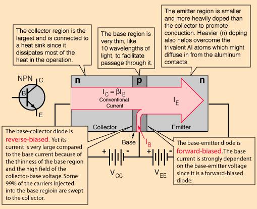
4 Transistor Structure
5 npn BJT I = I + E C I B V V BE CE = V = V B C V V E E Base-to-emitter pn junction is forward biased Base-to-collector pn junction is reverse biased Base is a very thin layer of p type region Emitter is more heavily n-doped than collector V > V > V C B E
6 Transistor as Current Amplifier The larger collector current I C is proportional to the base current I B according to the relationship I C =βi B, or more precisely it is proportional to the base-emitter voltage V BE. The smaller base current controls the larger collector current, achieving current amplification. The analogy to a valve is sometimes helpful. The smaller current in the base acts as a "valve", controlling the larger current from collector to emitter. A "signal" in the form of a variation in the base current is reproduced as a larger variation in the collector-to-emitter current, achieving an amplification of that signal. β is about 100 Amplification factor
7 pnp BJT Transistor Very thin

8 Transistor as Current Amplifier Constraints on Transistor Operation

9 BJT packages
10 Terminal characteristics of a typical BJT 0.2 V when saturation
11 Common emitter transistor circuit Transistor Characteristic Curves Controlled by collector circuit i c is proportional to i b 0.2 V when saturation

, useful for amplifier applications In saturation (collector a few tenths")
12 Transistors Transistor Operation Cut off (no collector current), useful for switch operation. In the active region (some collector current, more than a few tenths of a volt above the emitter), useful for amplifier applications In saturation (collector a few tenths of a volt above emitter), large current useful for "switch on" applications.
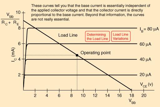
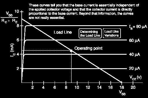
13 Transistors Transistor Characteristic Curves
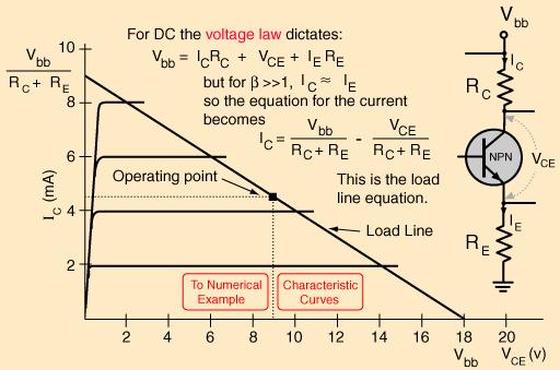
14 Transistors Transistor Characteristic Curves
15 Bipolar Transistor Switch V in =0.7V


16 Transistor Switch Example The base resistor is chosen small enough so that the base current drives the transistor into saturation. In this example the mechanical switch is used to produce the base current to close the transistor switch to show the principles. In practice, any voltage on the base sufficient to drive the transistor to saturation will close the switch and light the bulb. There is no current to the base, so the transistor is in the cut off condition with no collector current. All the voltage drop is across the transistor.


17 Transistor Switch Example NPN Common Emitter Switch For switching currents less than an ampere, the transistor switch can be used. Instead of a mechanical switch in the base circuit, an op-amp could be used. When the switch is open, no current flows in the base so the collector current is cut off. The resistor R B must be small enough to drive the transistor to saturation so that most of the voltage V cc appears across the load Rc. In a configuration where the output is taken below the load resistor, this kind of switch can function as an inverting buffer in digital circuits. For equal resistors, it has a gain of -1, and is used in digital circuits as an inverting buffer. A transistor switch with collector resistor can serve as an inverting buffer.

18 Transistor Switch Example Op-Amp Switching If an op-amp is used instead of a mechanical switch to operate a transistor switch. The diode is used for protection of the base-emitter junction in case the op-amp swings to its negative supply voltage.

19 LED Switch O V or 5V
20 Darlington Pair The emitter current of TR1 is the base current of TR2. A change in base current of TR1 can give a change 100 times larger in its emitter current. A change in the base current of TR2 has a similar effect on its emitter current. Therefore there is an overall amplification of 100 x 100 = times. This circuit is sometimes called the Super Alpha Pair. It is often used as a power output stage. The two transistors can come in the same package.
 and silicone dome (bottom) layouts - cross-section through a standard dual in-line")
21 Phototransistor and Optoisolator An electronic device designed to transfer electrical signals by utilizing light waves to provide coupling with electrical isolation between its input and output Planar (top) and silicone dome (bottom) layouts - cross-section through a standard dual in-line package
22 Guarantee a transistor in saturation Q:
23 Common emitter npn BJT
24 Common emitter npn BJT current amplifier The Common Emitter Amplifier Circuit This type of configuration is the most commonly used circuit for transistor based amplifiers and which represents the "normal" method of bipolar transistor connection.

25 Common emitter npn BJT current amplifier I = I + E C I B V > V > V C B E The collector current I C is proportional to the base current I B according to the relationship I C =βi B β has a value between 20 and 200 for most general purpose transistors
26 Common emitter npn BJT current amplifier

27 BJT current amplifier
28 Common base pnp BJT voltage amplifier Common base The BASE connection is common to both the input signal AND the output signal with the input signal being applied between the base and the emitter terminals. The corresponding output signal is taken from between the base and the collector terminals with the base terminal grounded. The input current flowing into the emitter is quite large as its the sum of both the base current and collector current respectively therefore, the collector current output is less than the emitter current input resulting in a current gain for this type of circuit of "1" (unity) or less, in other words the common base configuration "attenuates" the input signal.
29 pnp BJT voltage amplifier This type of amplifier configuration is a non-inverting voltage amplifier circuit, in that the signal voltages V in and V out are in-phase. This type of transistor arrangement is not very common due to its unusually high voltage gain characteristics due to its high ratio of output to input resistance or more importantly "load" resistance (R L ) to "input" resistance (R in ) giving it a value of "Resistance Gain". Then the voltage gain (Av for a common base configuration

30 Emitter Follower Circuit a large Current gain This type of configuration is commonly known as a Voltage Follower or Emitter Follower circuit. This type of bipolar transistor configuration is a non-inverting circuit in that the signal voltages of V in and V out are in-phase. It has a voltage gain that is always less than "1" (unity).

31 Emitter Follower Switch NPN Emitter Follower Switch The emitter follower can also be used for switching. The resistor R B must be small enough to drive the transistor to saturation so that most of the voltage V cc appears across the load.
32 Angular Position of a Robotic Scanner Photo-interrupter
Lecture 3: Transistors
 Lecture 3: Transistors Now that we know about diodes, let s put two of them together, as follows: collector base emitter n p n moderately doped lightly doped, and very thin heavily doped At first glance,
Transistors and Applications
 Chapter 17 Transistors and Applications DC Operation of Bipolar Junction Transistors (BJTs) The bipolar junction transistor (BJT) is constructed with three doped semiconductor regions separated by two
EXPERIMENT 5 CURRENT AND VOLTAGE CHARACTERISTICS OF BJT
 EXPERIMENT 5 CURRENT AND VOLTAGE CHARACTERISTICS OF BJT 1. OBJECTIVES 1.1 To practice how to test NPN and PNP transistors using multimeter. 1.2 To demonstrate the relationship between collector current
BJT. Bipolar Junction Transistor BJT BJT 11/6/2018. Dr. Satish Chandra, Assistant Professor, P P N College, Kanpur 1
 BJT Bipolar Junction Transistor Satish Chandra Assistant Professor Department of Physics P P N College, Kanpur www.satish0402.weebly.com The Bipolar Junction Transistor is a semiconductor device which
Transistor Characteristics
 Transistor Characteristics Topics covered in this presentation: Transistor Construction Transistor Operation Transistor Characteristics 1 of 15 The Transistor The transistor is a semiconductor device that
Lecture 12. Bipolar Junction Transistor (BJT) BJT 1-1
 BJT 1-1") Lecture 12 Bipolar Junction Transistor (BJT) BJT 1-1 Course Info Lecture hours: 4 Two Lectures weekly (Saturdays and Wednesdays) Location: K2 Time: 1:40 pm Tutorial hours: 2 One tutorial class every week
Lecture 12 Bipolar Junction Transistor (BJT) BJT 1-1 Course Info Lecture hours: 4 Two Lectures weekly (Saturdays and Wednesdays) Location: K2 Time: 1:40 pm Tutorial hours: 2 One tutorial class every week
EE105 Fall 2014 Microelectronic Devices and Circuits. NPN Bipolar Junction Transistor (BJT)
") EE105 Fall 2014 Microelectronic Devices and Circuits Prof. Ming C. Wu wu@eecs.berkeley.edu 511 utardja Dai Hall (DH) 1 NPN Bipolar Junction Transistor (BJT) Forward Bias Reverse Bias Hole Flow Electron
EE105 Fall 2014 Microelectronic Devices and Circuits Prof. Ming C. Wu wu@eecs.berkeley.edu 511 utardja Dai Hall (DH) 1 NPN Bipolar Junction Transistor (BJT) Forward Bias Reverse Bias Hole Flow Electron
Lecture (09) Bipolar Junction Transistor 3
 Bipolar Junction Transistor 3") Lecture (09) Bipolar Junction Transistor 3 By: Dr. Ahmed ElShafee ١ I THE BJT AS AN AMPLIFIER Amplification is the process of linearly increasing the amplitude of an electrical signal and is one of the
Lecture (09) Bipolar Junction Transistor 3 By: Dr. Ahmed ElShafee ١ I THE BJT AS AN AMPLIFIER Amplification is the process of linearly increasing the amplitude of an electrical signal and is one of the
Lecture 24: Bipolar Junction Transistors (1) Bipolar Junction Structure, Operating Regions, Biasing
 Bipolar Junction Structure, Operating Regions, Biasing") Lecture 24: Bipolar Junction Transistors (1) Bipolar Junction Structure, Operating Regions, Biasing BJT Structure the BJT is formed by doping three semiconductor regions (emitter, base, and collector)
Lecture 24: Bipolar Junction Transistors (1) Bipolar Junction Structure, Operating Regions, Biasing BJT Structure the BJT is formed by doping three semiconductor regions (emitter, base, and collector)
4.2.2 Metal Oxide Semiconductor Field Effect Transistor (MOSFET)
") 4.2.2 Metal Oxide Semiconductor Field Effect Transistor (MOSFET) The Metal Oxide Semitonductor Field Effect Transistor (MOSFET) has two modes of operation, the depletion mode, and the enhancement mode.
4.2.2 Metal Oxide Semiconductor Field Effect Transistor (MOSFET) The Metal Oxide Semitonductor Field Effect Transistor (MOSFET) has two modes of operation, the depletion mode, and the enhancement mode.
Chapter 3 Bipolar Junction Transistors (BJT)
") Chapter 3 Bipolar Junction Transistors (BJT) Transistors In analog circuits, transistors are used in amplifiers and linear regulated power supplies. In digital circuits they function as electrical switches,
Chapter 3 Bipolar Junction Transistors (BJT) Transistors In analog circuits, transistors are used in amplifiers and linear regulated power supplies. In digital circuits they function as electrical switches,
UNIT-III Bipolar Junction Transistor
 DC UNT-3.xplain the construction and working of JT. UNT- ipolar Junction Transistor A bipolar (junction) transistor (JT) is a three-terminal electronic device constructed of doped semiconductor material
Electronic Circuits - Tutorial 07 BJT transistor 1
 Electronic Circuits - Tutorial 07 BJT transistor 1-1 / 20 - T & F # Question 1 A bipolar junction transistor has three terminals. T 2 For operation in the linear or active region, the base-emitter junction
Electronics I Circuit Drawings. Robert R. Krchnavek Rowan University Spring, 2018
 Electronics I Circuit Drawings Robert R. Krchnavek Rowan University Spring, 2018 Ideal Diode Piecewise Linear Models of a Diode Piecewise Linear Models of a Diode 1 r d Piecewise Linear Models of a Diode
Analog & Digital Electronics Course No: PH-218
 Analog & Digital Electronics Course No: PH-218 Lec-5: Bipolar Junction Transistor (BJT) Course nstructors: Dr. A. P. VAJPEY Department of Physics, ndian nstitute of Technology Guwahati, ndia 1 Bipolar
Chapter 3. Bipolar Junction Transistors
 Chapter 3. Bipolar Junction Transistors Outline: Fundamental of Transistor Common-Base Configuration Common-Emitter Configuration Common-Collector Configuration Introduction The transistor is a three-layer
Concepts to be Covered
 Introductory Medical Device Prototyping Analog Circuits Part 2 Semiconductors, http://saliterman.umn.edu/ Department of Biomedical Engineering, University of Minnesota Concepts to be Covered Semiconductors
Chapter 3: Bipolar Junction Transistors
 Chapter 3: Bipolar Junction Transistors Transistor Construction There are two types of transistors: pnp npn pnp The terminals are labeled: E - Emitter B - Base C - Collector npn 2 Transistor Operation
THE METAL-SEMICONDUCTOR CONTACT
 THE METAL-SEMICONDUCTOR CONTACT PROBLEM 1 To calculate the theoretical barrier height, built-in potential barrier, and maximum electric field in a metal-semiconductor diode for zero applied bias. Consider
Mechatronics and Measurement. Lecturer:Dung-An Wang Lecture 2
 Mechatronics and Measurement Lecturer:Dung-An Wang Lecture 2 Lecture outline Reading:Ch3 of text Today s lecture Semiconductor 2 Diode 3 4 Zener diode Voltage-regulator diodes. This family of diodes exhibits
Bipolar Junction Transistors
 Bipolar Junction Transistors Invented in 1948 at Bell Telephone laboratories Bipolar junction transistor (BJT) - one of the major three terminal devices Three terminal devices more useful than two terminal
The shape of the waveform will be the same, but its level is shifted either upward or downward. The values of the resistor R and capacitor C affect
 Diode as Clamper A clamping circuit is used to place either the positive or negative peak of a signal at a desired level. The dc component is simply added or subtracted to/from the input signal. The clamper
Electronics EECE2412 Spring 2017 Exam #2
 Electronics EECE2412 Spring 2017 Exam #2 Prof. Charles A. DiMarzio Department of Electrical and Computer Engineering Northeastern University 30 March 2017 File:12198/exams/exam2 Name: : General Rules:
CHAPTER 3: BIPOLAR JUNCION TRANSISTOR DR. PHẠM NGUYỄN THANH LOAN
 CHAPTER 3: BIPOLAR JUNCION TRANSISTOR DR. PHẠM NGUYỄN THANH LOAN Hanoi, 9/24/2012 Contents 2 Structure and operation of BJT Different configurations of BJT Characteristic curves DC biasing method and analysis
EEE225: Analogue and Digital Electronics
 EEE225: Analogue and Digital Electronics Lecture I James E. Green Department of Electronic Engineering University of Sheffield j.e.green@sheffield.ac.uk Introduction This Lecture 1 Introduction Aims &
Figure1: Basic BJT construction.
 Chapter 4: Bipolar Junction Transistors (BJTs) Bipolar Junction Transistor (BJT) Structure The BJT is constructed with three doped semiconductor regions separated by two pn junctions, as in Figure 1(a).
Chapter 6: Transistors and Gain
 I. Introduction Chapter 6: Transistors and Gain This week we introduce the transistor. Transistors are three-terminal devices that can amplify a signal and increase the signal s power. The price is that
UNIT 3 Transistors JFET
 UNIT 3 Transistors JFET Mosfet Definition of BJT A bipolar junction transistor is a three terminal semiconductor device consisting of two p-n junctions which is able to amplify or magnify a signal. It
An Introduction to Bipolar Junction Transistors. Prepared by Dr Yonas M Gebremichael, 2005
 An Introduction to Bipolar Junction Transistors Transistors Transistors are three port devices used in most integrated circuits such as amplifiers. Non amplifying components we have seen so far, such as
COE/EE152: Basic Electronics. Lecture 5. Andrew Selasi Agbemenu. Outline
 COE/EE152: Basic Electronics Lecture 5 Andrew Selasi Agbemenu 1 Outline Physical Structure of BJT Two Diode Analogy Modes of Operation Forward Active Mode of BJTs BJT Configurations Early Effect Large
5.1 BJT Device Structure and Physical Operation
 11/28/2004 section 5_1 BJT Device Structure and Physical Operation blank 1/2 5.1 BJT Device Structure and Physical Operation Reading Assignment: pp. 377-392 Another kind of transistor is the Bipolar Junction
The first transistor. (Courtesy Bell Telephone Laboratories.)
") Fig. 3.1 The first transistor. (Courtesy Bell Telephone Laboratories.) Fig. 3.2 Types of transistors: (a) pnp; (b) npn. : (a) pnp; : (b) npn Fig. 3.3 Forward-biased junction of a pnp transistor. Fig. 3.4
Fig. 3.1 The first transistor. (Courtesy Bell Telephone Laboratories.) Fig. 3.2 Types of transistors: (a) pnp; (b) npn. : (a) pnp; : (b) npn Fig. 3.3 Forward-biased junction of a pnp transistor. Fig. 3.4
Analog Electronics. Electronic Devices, 9th edition Thomas L. Floyd Pearson Education. Upper Saddle River, NJ, All rights reserved.
 Analog Electronics BJT Structure The BJT has three regions called the emitter, base, and collector. Between the regions are junctions as indicated. The base is a thin lightly doped region compared to the
ET215 Devices I Unit 4A
 ITT Technical Institute ET215 Devices I Unit 4A Chapter 3, Section 3.1-3.2 This unit is divided into two parts; Unit 4A and Unit 4B Chapter 3 Section 3.1 Structure of Bipolar Junction Transistors The basic
EXPERIMENT 12: SIMULATION STUDY OF DIFFERENT BIASING CIRCUITS USING NPN BJT
 EXPERIMENT 12: SIMULATION STUDY OF DIFFERENT BIASING CIRCUITS USING NPN BJT AIM: 1) To study different BJT DC biasing circuits 2) To design voltage divider bias circuit using NPN BJT SOFTWARE TOOL: PC
Lecture 9 Transistors
 Lecture 9 Transistors Physics Transistor/transistor logic CMOS logic CA 1947 http://www.extremetech.com/extreme/164301-graphenetransistors-based-on-negative-resistance-could-spell-theend-of-silicon-and-semiconductors
Transistor fundamentals Nafees Ahamad
 Transistor fundamentals Nafees Ahamad Asstt. Prof., EECE Deptt, DIT University, Dehradun Website: www.eedofdit.weebly.com Transistor A transistor consists of two PN junctions formed by sandwiching either
Lecture (06) Bipolar Junction Transistor
 Bipolar Junction Transistor") Lecture (06) Bipolar Junction Transistor By: Dr. Ahmed lshafee ١ Agenda BJT structure BJT operation BJT characteristics ٢ BJT structure The BJT is constructed with three doped semiconductor regions One
Lecture (06) Bipolar Junction Transistor By: Dr. Ahmed lshafee ١ Agenda BJT structure BJT operation BJT characteristics ٢ BJT structure The BJT is constructed with three doped semiconductor regions One
BJT Characteristics & Common Emitter Transistor Amplifier
 LAB #07 Objectives 1. To graph the collector characteristics of a transistor. 2. To measure AC and DC voltages in a common-emitter amplifier. Theory BJT A bipolar (junction) transistor (BJT) is a three-terminal
Lecture #3 BJT Transistors & DC Biasing
 November 2014 Ahmad El-Banna Integrated Technical Education Cluster At AlAmeeria J-601-1448 Electronic Principals Lecture #3 BJT Transistors & DC Biasing Instructor: Dr. Ahmad El-Banna Agenda Transistor
Transistor electronic technologies
 Transistor electronic technologies Bipolar Junction Transistor discrete or integrated circuit discrete = individual component MOS (Metal-Oxide-Silicon) Field Effect Transistor mainly used in integrated
PHY405F 2009 EXPERIMENT 6 SIMPLE TRANSISTOR CIRCUITS
 PHY405F 2009 EXPERIMENT 6 SIMPLE TRANSISTOR CIRCUITS Due Date (NOTE CHANGE): Thursday, Nov 12 th @ 5 pm; Late penalty in effect! Most active electronic devices are based on the transistor as the fundamental
BIPOLAR JUNCTION TRANSISTORS (BJTs) Dr Derek Molloy, DCU
 Dr Derek Molloy, DCU") IPOLAR JUNCTION TRANSISTORS (JTs) Dr Derek Molloy, DCU What are JTs? Two PN junctions joined together is a JT Simply known as a transistor! ipolar? Current carried by electrons and holes Will see FETs
IPOLAR JUNCTION TRANSISTORS (JTs) Dr Derek Molloy, DCU What are JTs? Two PN junctions joined together is a JT Simply known as a transistor! ipolar? Current carried by electrons and holes Will see FETs
Bipolar Junction Transistor (BJT)
") Bipolar Junction Transistor (BJT) - three terminal device - output port controlled by current flow into input port Structure - three layer sandwich of n-type and p-type material - npn and pnp transistors
Bipolar Junction Transistor (BJT) - three terminal device - output port controlled by current flow into input port Structure - three layer sandwich of n-type and p-type material - npn and pnp transistors
Dr. Charles Kim ELECTRONICS I. Lab 5 Bipolar Junction Transistor (BJT) I TRADITIONAL LAB
 I TRADITIONAL LAB") ELECTRONICS I Lab 5 Bipolar Junction Transistor (BJT) I TRADITIONAL LAB MOBILE STUDIO LAB Before We Start A transistor is a 3-terminal device available in two configurations, NPN and PNP. The transistor
ELECTRONICS I Lab 5 Bipolar Junction Transistor (BJT) I TRADITIONAL LAB MOBILE STUDIO LAB Before We Start A transistor is a 3-terminal device available in two configurations, NPN and PNP. The transistor
ECE 334: Electronic Circuits Lecture 2: BJT Large Signal Model
 Faculty of Engineering ECE 334: Electronic Circuits Lecture 2: BJT Large Signal Model Agenda I & V Notations BJT Devices & Symbols BJT Large Signal Model 2 I, V Notations (1) It is critical to understand
Analytical Chemistry II
 Analytical Chemistry II L3: Signal processing (selected slides) Semiconductor devices Apart from resistors and capacitors, electronic circuits often contain nonlinear devices: transistors and diodes. The
BJT Amplifier. Superposition principle (linear amplifier)
") BJT Amplifier Two types analysis DC analysis Applied DC voltage source AC analysis Time varying signal source Superposition principle (linear amplifier) The response of a linear amplifier circuit excited
BJT Amplifier Two types analysis DC analysis Applied DC voltage source AC analysis Time varying signal source Superposition principle (linear amplifier) The response of a linear amplifier circuit excited
Bipolar junction transistors.
 Bipolar junction transistors. Third Semester Course code : 15EECC202 Analog electronic circuits (AEC) Team: Dr. Nalini C Iyer, R.V. Hangal, Sujata N, Prashant A, Sneha Meti AEC Team, Faculty, School of
BFF1303: ELECTRICAL / ELECTRONICS ENGINEERING. Analog Electronics: Bipolar Junction Transistors
 BFF1303: ELECTRICAL / ELECTRONICS ENGINEERING Analog Electronics: Bipolar Junction Transistors Ismail Mohd Khairuddin, Zulkifil Md Yusof Faculty of Manufacturing Engineering Universiti Malaysia Pahang
PHYS225 Lecture 6. Electronic Circuits
 PHYS225 Lecture 6 Electronic Circuits Transistors History Basic physics of operation Ebers-Moll model Small signal equivalent Last lecture Introduction to Transistors A transistor is a device with three
(a) BJT-OPERATING MODES & CONFIGURATIONS
 BJT-OPERATING MODES & CONFIGURATIONS") (a) BJT-OPERATING MODES & CONFIGURATIONS 1. The leakage current I CBO flows in (a) The emitter, base and collector leads (b) The emitter and base leads. (c) The emitter and collector leads. (d) The base
(a) BJT-OPERATING MODES & CONFIGURATIONS 1. The leakage current I CBO flows in (a) The emitter, base and collector leads (b) The emitter and base leads. (c) The emitter and collector leads. (d) The base
ITT Technical Institute. ET215 Devices 1. Unit 6 Chapter 3, Sections
 ITT Technical Institute ET215 Devices 1 Unit 6 Chapter 3, Sections 3.7-3.9 Chapter 3 Section 3.7 The Bipolar Transistor as a Switch Objectives: Explain how a transistor can be used as a switch 1. Compute
ECE 440 Lecture 29 : Introduction to the BJT-I Class Outline:
 ECE 440 Lecture 29 : Introduction to the BJT-I Class Outline: Narrow-Base Diode BJT Fundamentals BJT Amplification Things you should know when you leave Key Questions How does the narrow-base diode multiply
Electronics Fundamentals BIPOLAR TRANSISTORS. Construction, circuit symbols and biasing examples for NPN and PNP junction transistors.
 IPOLA TANSISTOS onstruction, circuit symbols and biasing examples for NPN and PNP junction transistors Slide 1 xternal bias voltages create an electric field, which pulls electrons (emitted into the base
Chapter Two "Bipolar Transistor Circuits"
 Chapter Two "Bipolar Transistor Circuits" 1.TRANSISTOR CONSTRUCTION:- The transistor is a three-layer semiconductor device consisting of either two n- and one p-type layers of material or two p- and one
N9-1. Gain. Input and Output Impedances. Amplifier Types. Z out. Z in = AH( jω)
") Amplification We have seen in earlier notes that a carbon composition resistor continuously dissipates heat to the environment. Most circuit elements do likewise to some degree, including the capacitor
Amplification We have seen in earlier notes that a carbon composition resistor continuously dissipates heat to the environment. Most circuit elements do likewise to some degree, including the capacitor
EXPERIMENT 6 REPORT Bipolar Junction Transistor (BJT) Characteristics
 Characteristics") Name & Surname: ID: Date: EXPERIMENT 6 REPORT Bipolar Junction Transistor (BJT) Characteristics Objectives: 1. To determine transistor type (npn, pnp),terminals, and material using a DMM 2. To graph the
Name & Surname: ID: Date: EXPERIMENT 6 REPORT Bipolar Junction Transistor (BJT) Characteristics Objectives: 1. To determine transistor type (npn, pnp),terminals, and material using a DMM 2. To graph the
ECE321 Electronics I Fall 2006
 ECE321 Electronics I Fall 2006 Professor James E. Morris Lecture 11 31 st October, 2006 Bipolar Junction Transistors (BJTs) 5.1 Device Structure & Physics 5.2 I-V Characteristics Convert 5.1 information
7. Bipolar Junction Transistor
 41 7. Bipolar Junction Transistor 7.1. Objectives - To experimentally examine the principles of operation of bipolar junction transistor (BJT); - To measure basic characteristics of n-p-n silicon transistor
Physics of Bipolar Transistor
 Physics of Bipolar Transistor Motivations - In many electronic applications, amplifier is the most fundamental building block. Ex Audio amplifier: amplifies electric signal to drive a speaker RF Power
Lecture #3 ( 2 weeks) Transistors
 Transistors") Spring 2015 Benha University Faculty of Engineering at Shoubra ECE-291 Electronic Engineering Lecture #3 ( 2 weeks) Transistors Instructor: Dr. Ahmad El-Banna 1 Agenda BJT Structure Basic Operation Transistor
Spring 2015 Benha University Faculty of Engineering at Shoubra ECE-291 Electronic Engineering Lecture #3 ( 2 weeks) Transistors Instructor: Dr. Ahmad El-Banna 1 Agenda BJT Structure Basic Operation Transistor
KOM2751 Analog Electronics :: Dr. Muharrem Mercimek :: YTU - Control and Automation Dept. 1 2 (CONT D - II) DIODE APPLICATIONS
 DIODE APPLICATIONS") KOM2751 Analog Electronics :: Dr. Muharrem Mercimek :: YTU - Control and Automation Dept. 1 2 (CONT D - II) DIODE APPLICATIONS Most of the content is from the textbook: Electronic devices and circuit theory,
KOM2751 Analog Electronics :: Dr. Muharrem Mercimek :: YTU - Control and Automation Dept. 1 2 (CONT D - II) DIODE APPLICATIONS Most of the content is from the textbook: Electronic devices and circuit theory,
C H A P T E R 6 Bipolar Junction Transistors (BJTs)
") C H A P T E R 6 Bipolar Junction Transistors (BJTs) Figure 6.1 A simplified structure of the npn transistor and pnp transistor. Table 6.1: BJT modes of Operation Mode EBJ CBJ Cutoff Reverse Reverse Active
C H A P T E R 6 Bipolar Junction Transistors (BJTs) Figure 6.1 A simplified structure of the npn transistor and pnp transistor. Table 6.1: BJT modes of Operation Mode EBJ CBJ Cutoff Reverse Reverse Active
ECE 310 Microelectronics Circuits
 ECE 310 Microelectronics Circuits Bipolar Transistors Dr. Vishal Saxena (vishalsaxena@boisetstate.edu) Jan 20, 2014 Vishal Saxena 1 Bipolar Transistor n the chapter, we will study the physics of bipolar
b b Fig. 1 Transistor symbols
 TRANSISTORS Transistors have three terminals which are referred to as emitter (e), base (b) and collector (c). Fig 1 shows the symbols used for the two types of transistors in common use. c c b b e e npn
Analog Circuits Prof. Jayanta Mukherjee Department of Electrical Engineering Indian Institute of Technology - Bombay
 Analog Circuits Prof. Jayanta Mukherjee Department of Electrical Engineering Indian Institute of Technology - Bombay Week - 08 Module - 04 BJT DC Circuits Hello, welcome to another module of this course
Electronic Circuits ELCT604 (Spring 2018) Lecture 2 BJT Amplifiers
 Lecture 2 BJT Amplifiers") Electronic Circuits ELCT604 (Spring 2018) Lecture 2 BJT Amplifiers Assistant Professor Office: C3.315 E-mail: eman.azab@guc.edu.eg 1 Analog Voltage Amplifiers Circuit Design and Configurations 2 Objective
Electronic Circuits ELCT604 (Spring 2018) Lecture 2 BJT Amplifiers Assistant Professor Office: C3.315 E-mail: eman.azab@guc.edu.eg 1 Analog Voltage Amplifiers Circuit Design and Configurations 2 Objective
EIE209 Basic Electronics. Transistor Devices. Contents BJT and FET Characteristics Operations. Prof. C.K. Tse: T ransistor devices
 EIE209 Basic Electronics Transistor Devices Contents BJT and FET Characteristics Operations 1 What is a transistor? Three-terminal device whose voltage-current relationship is controlled by a third voltage
UNIT I Introduction to DC & AC circuits
 SIDDHARTH GROUP OF INSTITUTIONS :: PUTTUR Siddharth Nagar, Narayanavanam Road 517583 QUESTION BANK (DESCRIPTIVE) Subject with Code: Basic Electrical and Electronics Engineering (16EE207) Year & Sem: II-B.
ME 4447 / 6405 Student Lecture. Transistors. Abiodun Otolorin Michael Abraham Waqas Majeed
 ME 4447 / 6405 Student Lecture Transistors Abiodun Otolorin Michael Abraham Waqas Majeed Lecture Overview Transistor? History Underlying Science Properties Types of transistors Bipolar Junction Transistors
Analog Circuits Part 2 Semiconductors
 Introductory Medical Device Prototyping Analog Circuits Part 2 Semiconductors, http://saliterman.umn.edu/ Department of Biomedical Engineering, University of Minnesota Concepts to be Covered Semiconductors
Student Lecture by: Giangiacomo Groppi Joel Cassell Pierre Berthelot September 28 th 2004
 Student Lecture by: Giangiacomo Groppi Joel Cassell Pierre Berthelot September 28 th 2004 Lecture outline Historical introduction Semiconductor devices overview Bipolar Junction Transistor (BJT) Field
ชาว ศวกรรมคอมพ วเตอร คณะว ศวกรรมศาสตร มหาว ทยาล ยเทคโนโลย ราชมงคลพระนคร
 EN2042102 วงจรไฟฟ าและอ เล กทรอน กส Circuits and Electronics บทท 7 ทรานซ สเตอร Bipolar Junction Transistor สาขาว ชาว ศวกรรมคอมพ วเตอร คณะว ศวกรรมศาสตร มหาว ทยาล ยเทคโนโลย ราชมงคลพระนคร Objectives Describe
Operational Amplifiers
 Operational Amplifiers November 23, 2017 1 Pre-lab Calculations 1) Calculate the gain for all four circuits in Fig. 3. 2 Introduction Operational Amplifiers? They should call them fun amplifiers. Because,
Course Roadmap Rectification Bipolar Junction Transistor
 Course oadmap ectification Bipolar Junction Transistor Acnowledgements: Neamen, Donald: Microelectronics Circuit Analysis and Design, 3 rd Edition 6.101 Spring 2017 Lecture 3 1 6.101 Spring 2017 Lecture
SRM INSTITUTE OF SCIENCE AND TECHNOLOGY (DEEMED UNIVERSITY)
") SRM INSTITUTE OF SCIENCE AND TECHNOLOGY (DEEMED UNIVERSITY) QUESTION BANK I YEAR B.Tech (II Semester) ELECTRONIC DEVICES (COMMON FOR EC102, EE104, IC108, BM106) UNIT-I PART-A 1. What are intrinsic and
SRM INSTITUTE OF SCIENCE AND TECHNOLOGY (DEEMED UNIVERSITY) QUESTION BANK I YEAR B.Tech (II Semester) ELECTRONIC DEVICES (COMMON FOR EC102, EE104, IC108, BM106) UNIT-I PART-A 1. What are intrinsic and
Field Effect Transistors
 Field Effect Transistors Purpose In this experiment we introduce field effect transistors (FETs). We will measure the output characteristics of a FET, and then construct a common-source amplifier stage,
Electronic Circuits for Mechatronics ELCT 609 Lecture 5: BJT Voltage Amplifiers
 Electronic Circuits for Mechatronics ELCT 609 Lecture 5: BJT Voltage Amplifiers Assistant Professor Office: C3.315 E-mail: eman.azab@guc.edu.eg 1 BJT Modes of Operation Electrical Equations of BJT 2 BJT
Lab no. 4 Bipolar Transistor (NPN and PNP)
") Lab no. 4 Bipolar Transistor (NPN and PNP) Transistors are semiconductor devices that enable to control the flow of large current by much smaller current. Bipolar transistor consists of three areas of
Lab no. 4 Bipolar Transistor (NPN and PNP) Transistors are semiconductor devices that enable to control the flow of large current by much smaller current. Bipolar transistor consists of three areas of
EE 330 Laboratory 8 Discrete Semiconductor Amplifiers
 EE 330 Laboratory 8 Discrete Semiconductor Amplifiers Fall 2018 Contents Objective:...2 Discussion:...2 Components Needed:...2 Part 1 Voltage Controlled Amplifier...2 Part 2 A Nonlinear Application...3
Basic Electronics Prof. Dr. Chitralekha Mahanta Department of Electronics and Communication Engineering Indian Institute of Technology, Guwahati
 Basic Electronics Prof. Dr. Chitralekha Mahanta Department of Electronics and Communication Engineering Indian Institute of Technology, Guwahati Module: 2 Bipolar Junction Transistors Lecture-1 Transistor
Chapter 3: TRANSISTORS. Dr. Gopika Sood PG Govt. College For Girls Sector -11, Chandigarh
 Chapter 3: TRANSISTORS Dr. Gopika Sood PG Govt. College For Girls Sector -11, Chandigarh OUTLINE Transistors Bipolar Junction Transistor (BJT) Operation of Transistor Transistor parameters Load Line Biasing
ANALOG FUNDAMENTALS C. Topic 4 BASIC FET AMPLIFIER CONFIGURATIONS
 AV18-AFC ANALOG FUNDAMENTALS C Topic 4 BASIC FET AMPLIFIER CONFIGURATIONS 1 ANALOG FUNDAMENTALS C AV18-AFC Overview This topic identifies the basic FET amplifier configurations and their principles of
Transistors. electrons N P N holes. Base. An NPN device makes a transistor
 NPN Transistor Theory Transistors Transistors are similar to diodes in that they are made up on ntype and ptype silicon. They differ in that Transistors are 3terminal devices (NPN or PNP), Transistors
Bipolar Junction Transistors (BJTs) Overview
 Overview") 1 Bipolar Junction Transistors (BJTs) Asst. Prof. MONTREE SIRIPRUCHYANUN, D. Eng. Dept. of Teacher Training in Electrical Engineering, Faculty of Technical Education King Mongkut s Institute of Technology
1 Bipolar Junction Transistors (BJTs) Asst. Prof. MONTREE SIRIPRUCHYANUN, D. Eng. Dept. of Teacher Training in Electrical Engineering, Faculty of Technical Education King Mongkut s Institute of Technology
Prof. Anyes Taffard. Physics 120/220. Diode Transistor
 Prof. Anyes Taffard Physics 120/220 Diode Transistor Diode One can think of a diode as a device which allows current to flow in only one direction. Anode I F Cathode stripe Diode conducts current in this
MTLE-6120: Advanced Electronic Properties of Materials. Semiconductor transistors for logic and memory. Reading: Kasap
 MTLE-6120: Advanced Electronic Properties of Materials 1 Semiconductor transistors for logic and memory Reading: Kasap 6.6-6.8 Vacuum tube diodes 2 Thermionic emission from cathode Electrons collected
University of Southern C alifornia School Of Engineering Department Of Electrical Engineering
 University of Southern C alifornia School Of Engineering Department Of Electrical Engineering EE 348: Homework Assignment #04 Spring, 2001 (Due 02/27/2001) Choma Problem #16: n monolithic circuits, diodes
Practical 2P12 Semiconductor Devices
 Practical 2P12 Semiconductor Devices What you should learn from this practical Science This practical illustrates some points from the lecture courses on Semiconductor Materials and Semiconductor Devices
PART-A UNIT I Introduction to DC & AC circuits
 SIDDHARTH GROUP OF INSTITUTIONS :: PUTTUR (AUTONOMOUS) Siddharth Nagar, Narayanavanam Road 517583 QUESTION BANK (DESCRIPTIVE) Subject with Code : Basic Electrical and Electronics Engineering (16EE207)
Single-Stage BJT Amplifiers and BJT High-Frequency Model. Single-Stage BJT Amplifier Configurations
 1 Single-Stage BJT Amplifiers and BJT High-Frequency Model Asst. Prof. MONTREE SIRIPRUCHYANUN, D. Eng. Dept. of Teacher Training in Electrical Engineering, Faculty of Technical Education King Mongkut s
Communication Microelectronics (W17)
") Communication Microelectronics (W17) Lecture 4: Bipolar Junction Transistor Assistant Professor Office: C3.315 E-mail: eman.azab@guc.edu.eg 1 Bipolar Junction Transistor (BJT) Physical Structure and I-V
Communication Microelectronics (W17) Lecture 4: Bipolar Junction Transistor Assistant Professor Office: C3.315 E-mail: eman.azab@guc.edu.eg 1 Bipolar Junction Transistor (BJT) Physical Structure and I-V
UNIT-1 Bipolar Junction Transistors. Text Book:, Microelectronic Circuits 6 ed., by Sedra and Smith, Oxford Press
 UNIT-1 Bipolar Junction Transistors Text Book:, Microelectronic Circuits 6 ed., by Sedra and Smith, Oxford Press Figure 6.1 A simplified structure of the npn transistor. Microelectronic Circuits, Sixth
SAMPLE FINAL EXAMINATION FALL TERM
 ENGINEERING SCIENCES 154 ELECTRONIC DEVICES AND CIRCUITS SAMPLE FINAL EXAMINATION FALL TERM 2001-2002 NAME Some Possible Solutions a. Please answer all of the questions in the spaces provided. If you need
Objective: To study and verify the functionality of a) PN junction diode in forward bias. Sl.No. Name Quantity Name Quantity 1 Diode
 PN junction diode in forward bias. Sl.No. Name Quantity Name Quantity 1 Diode") Experiment No: 1 Diode Characteristics Objective: To study and verify the functionality of a) PN junction diode in forward bias Components/ Equipments Required: b) Point-Contact diode in reverse bias Components
Experiment No: 1 Diode Characteristics Objective: To study and verify the functionality of a) PN junction diode in forward bias Components/ Equipments Required: b) Point-Contact diode in reverse bias Components
Practical 2P12 Semiconductor Devices
 Practical 2P12 Semiconductor Devices What you should learn from this practical Science This practical illustrates some points from the lecture courses on Semiconductor Materials and Semiconductor Devices
10 Semiconductors - Transistors
 10 Semiconductors - Transistors The transistor was invented in the late 1940s. Credit for its invention is given to three Bell Laboratories scientists, John Bardeen, Walter Brattain, and William Shockley.
Bipolar Junction Transistors (BJTs)
") C H A P T E R 6 Bipolar Junction Transistors (BJTs) Figure 6.1 A simplified structure of the npn transistor and pnp transistor. Table 6.1: BJT modes of Operation Mode Cutoff Active Saturation EBJ Reverse
C H A P T E R 6 Bipolar Junction Transistors (BJTs) Figure 6.1 A simplified structure of the npn transistor and pnp transistor. Table 6.1: BJT modes of Operation Mode Cutoff Active Saturation EBJ Reverse
Lecture 4. Reading: Chapter EE105 Fall 2007 Lecture 4, Slide 1 Prof. Liu, UC Berkeley
 Lecture 4 OUTLNE Bipolar Junction Transistor (BJT) General considerations Structure Operation in active mode Large-signal model and - characteristics Reading: Chapter 4.1-4.4.2 EE105 Fall 2007 Lecture