Capacitors, diodes, transistors
|
|
|
- Poppy Clark
- 5 years ago
- Views:
Transcription
1 Capacitors, diodes, transistors capacitors charging and time response filters (impedance) semi-conductor diodes rectifiers transformers transistors CHM6158C - Lecture 3 1
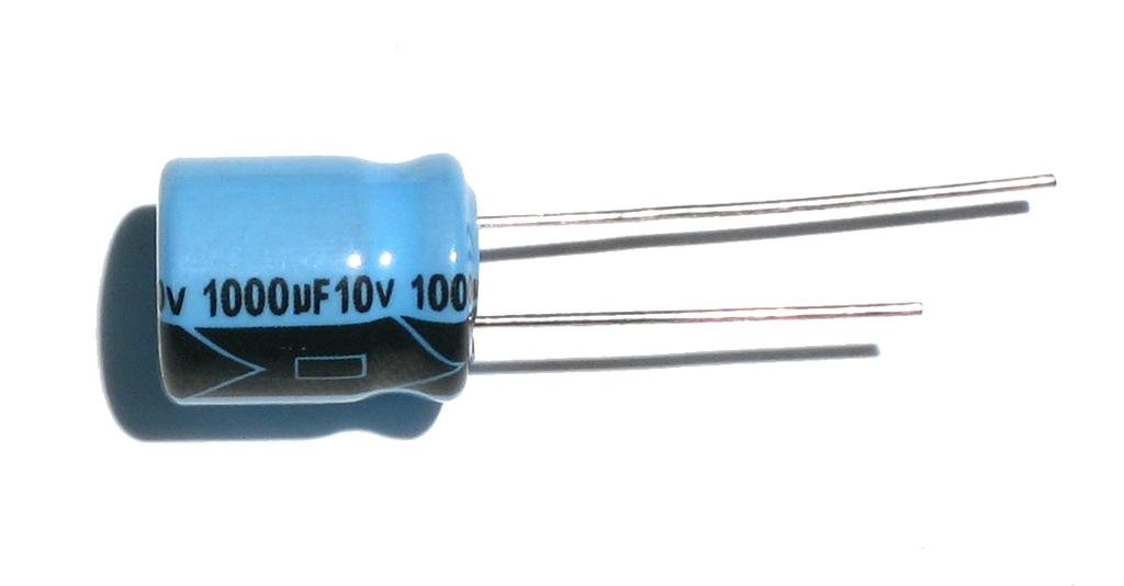
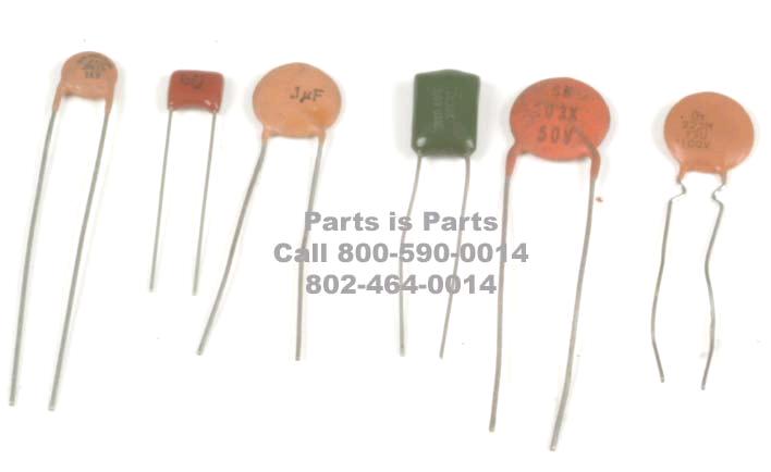
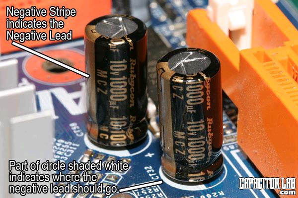
2 Capacitors Symbol 2
 = C/V (electrical charge that can be built up for a particular voltage) Typically µf (10-6 ), nf (10-9 ), pf (10-12 ) Dielectric material = insulating material that")
3 Capacitors Device consisting of two conducting plates separated by an insulating material By e.g. pulling away electrons from one side (Q+), build up electric field, which pulls electrons onto Q-. Unit of capacitance is Farad (F) = C/V (electrical charge that can be built up for a particular voltage) Typically µf (10-6 ), nf (10-9 ), pf (10-12 ) Dielectric material = insulating material that contains polar molecules that orient with the electric field (energy storage) What is the resistance of a capacitor? 3
4 Charging up a capacitor takes time RC circuit Every circuit has a resistance, which slows down the flow of electrons What will be the DC potential here? V = Vi ( 1 exp( t / RC)) Why? What will the current plot as a function of time look like? 4
5 Capacitors in parallel Electron flow from the same circuit has access to both sides of the capacitors Capacitances in parallel add up like resistors in series. N 1 C total = ( C i ) e.g. C 1 = µf, C 2 = µf and C 3 = µf, what is the total capacitance? 5
6 Capacitors in series Electron flow from the same circuit do NOT have access to both sides of the capacitors Capacitances in series add up like resistors in parallel. N 1 1 = Ctotal 1 C i Total capacitance lower than sum of capacitances. capacitors adversely affect each others ability to store charge. e.g. C 1 = µf, C 2 = µf, what is the total capacitance? 6

7 AC and capacitors In alternating current, orientation of electron flow keeps changing. What will happen if RC time constant is slower than AC frequency? i = C dv dt Note that current leads voltage by 90 o. 7
8 Voltage response At any moment in time, total voltage V r + V c = E, but relative voltages for V r and V c change as a function of time. Remember that V c as a function of time looks like this: What will be corresponding voltage across resistor as a function of time? What is RC in this case? 8

9 Voltage response Initially, total voltage on resistor why? What will happen for an ac voltage source, if frequency is low, frequency is high? Topics/DC-Current/gifs/Circuits50.gif 9
10 High- and low- pass filter For high-frequency signal, where will signal be transmitted? For low-frequency signal, where will signal be transmitted? More on noise and filters later 10
11 Note on impedance: AC equivalent of DC resistance Impedance = measure of opposition to alternating current What does voltage response compared to current look like? AC voltage source 11
12 Pure resistance circuit: Impedance For capacitance-only circuit: Current leads voltage i = C dv dt Does this make sense based on formula? More on impedance in lecture 17 12
13 + - (Semi- conductor) Diodes What happens here? doped material causes local charge imbalance between P (holes) and N (electrons) in forward bias, holes and electrons combine at P-N junction in reverse bias, a depletion region is created, which impedes conductance current flow occurs in one direction only 13
 What will the DC voltage look like? How can this voltage be made more continuous? 14")
14 ApplicaQon: RecQfier circuits: AC DC Only ac phase in forward direction leads to flow of current Draw which way does electricity flows (i.e., holes) What will the DC voltage look like? How can this voltage be made more continuous? 14
15 RC circuit to create smoother DC RC >> 1/f 15

16 Transformer: converqng ac voltage No. of coils V S N = S V N P P Principle of. 115 V ac converted to 12 VDC: Notice that current in secondary winding flows in opposite direction 115 ac 16

17 BJT (Bipolar JuncQon Transistor) Transistor = device that switches or amplifies electronic signals NPN transistor = two diodes with a shared anode (+) 17
18 BJT (Bipolar JuncQon Transistor) Bipolar junction transistor (BJT): pnp or npn Base current I B controls collector current I C. I C = β I B Common emitter circuit: Note design of pnp junction to allow much larger current flow from emitter to collector (i.e., very narrow n layer) 6th Ed., Douglas A. Skoog, F. James Holler and Stanley R. Crouch, Thomson Brooks/Cole, Gain 18

19 NPN transistor: common base Smaller current (base-emitter) acts as a gate to allow a larger current (collector-emitter). Collector-emitter current α base-emitter current Gate: base-emitter Larger current: collector-emitter Draw this circuit diagram Source: Wikipedia 19
20 Transistor amplifies current Collector current I C is h FE times larger than base current I B I C = h FE I B Art of Electronics 20
, which are at the basis")
21 Other examples Common collector circuit Which way does I B flow? Transistors are essential units in integrated circuits (IC s), which are at the basis of computer operation. 21
Lecture 12. Bipolar Junction Transistor (BJT) BJT 1-1
 BJT 1-1") Lecture 12 Bipolar Junction Transistor (BJT) BJT 1-1 Course Info Lecture hours: 4 Two Lectures weekly (Saturdays and Wednesdays) Location: K2 Time: 1:40 pm Tutorial hours: 2 One tutorial class every week
Lecture 12 Bipolar Junction Transistor (BJT) BJT 1-1 Course Info Lecture hours: 4 Two Lectures weekly (Saturdays and Wednesdays) Location: K2 Time: 1:40 pm Tutorial hours: 2 One tutorial class every week
Physics of Bipolar Transistor
 Physics of Bipolar Transistor Motivations - In many electronic applications, amplifier is the most fundamental building block. Ex Audio amplifier: amplifies electric signal to drive a speaker RF Power
Lecture 3: Transistors
 Lecture 3: Transistors Now that we know about diodes, let s put two of them together, as follows: collector base emitter n p n moderately doped lightly doped, and very thin heavily doped At first glance,
Lesson 5. Electronics: Semiconductors Doping p-n Junction Diode Half Wave and Full Wave Rectification Introduction to Transistors-
 Lesson 5 Electronics: Semiconductors Doping p-n Junction Diode Half Wave and Full Wave Rectification Introduction to Transistors- Types and Connections Semiconductors Semiconductors If there are many free
EXPERIMENT 5 CURRENT AND VOLTAGE CHARACTERISTICS OF BJT
 EXPERIMENT 5 CURRENT AND VOLTAGE CHARACTERISTICS OF BJT 1. OBJECTIVES 1.1 To practice how to test NPN and PNP transistors using multimeter. 1.2 To demonstrate the relationship between collector current
Lecture 24: Bipolar Junction Transistors (1) Bipolar Junction Structure, Operating Regions, Biasing
 Bipolar Junction Structure, Operating Regions, Biasing") Lecture 24: Bipolar Junction Transistors (1) Bipolar Junction Structure, Operating Regions, Biasing BJT Structure the BJT is formed by doping three semiconductor regions (emitter, base, and collector)
Lecture 24: Bipolar Junction Transistors (1) Bipolar Junction Structure, Operating Regions, Biasing BJT Structure the BJT is formed by doping three semiconductor regions (emitter, base, and collector)
Electronics I Circuit Drawings. Robert R. Krchnavek Rowan University Spring, 2018
 Electronics I Circuit Drawings Robert R. Krchnavek Rowan University Spring, 2018 Ideal Diode Piecewise Linear Models of a Diode Piecewise Linear Models of a Diode 1 r d Piecewise Linear Models of a Diode
Lecture - 18 Transistors
 Electronic Materials, Devices and Fabrication Dr. S. Prarasuraman Department of Metallurgical and Materials Engineering Indian Institute of Technology, Madras Lecture - 18 Transistors Last couple of classes
Prof. Anyes Taffard. Physics 120/220. Diode Transistor
 Prof. Anyes Taffard Physics 120/220 Diode Transistor Diode One can think of a diode as a device which allows current to flow in only one direction. Anode I F Cathode stripe Diode conducts current in this
Objective Type Questions 1. Why pure semiconductors are insulators at 0 o K? 2. What is effect of temperature on barrier voltage? 3.
 Objective Type Questions 1. Why pure semiconductors are insulators at 0 o K? 2. What is effect of temperature on barrier voltage? 3. What is difference between electron and hole? 4. Why electrons have
BJT Characteristics & Common Emitter Transistor Amplifier
 LAB #07 Objectives 1. To graph the collector characteristics of a transistor. 2. To measure AC and DC voltages in a common-emitter amplifier. Theory BJT A bipolar (junction) transistor (BJT) is a three-terminal
Experiment No. 9 DESIGN AND CHARACTERISTICS OF COMMON BASE AND COMMON COLLECTOR AMPLIFIERS
 Experiment No. 9 DESIGN AND CHARACTERISTICS OF COMMON BASE AND COMMON COLLECTOR AMPLIFIERS 1. Objective: The objective of this experiment is to explore the basic applications of the bipolar junction transistor
Diode conducts when V anode > V cathode. Positive current flow. Diodes (and transistors) are non-linear device: V IR!
 are non-linear device: V IR!") Diodes: What do we use diodes for? Lecture 5: Diodes and Transistors protect circuits by limiting the voltage (clipping and clamping) turn AC into DC (voltage rectifier) voltage multipliers (e.g. double
Diodes: What do we use diodes for? Lecture 5: Diodes and Transistors protect circuits by limiting the voltage (clipping and clamping) turn AC into DC (voltage rectifier) voltage multipliers (e.g. double
Chapter 3. Bipolar Junction Transistors
 Chapter 3. Bipolar Junction Transistors Outline: Fundamental of Transistor Common-Base Configuration Common-Emitter Configuration Common-Collector Configuration Introduction The transistor is a three-layer
ECE 334: Electronic Circuits Lecture 2: BJT Large Signal Model
 Faculty of Engineering ECE 334: Electronic Circuits Lecture 2: BJT Large Signal Model Agenda I & V Notations BJT Devices & Symbols BJT Large Signal Model 2 I, V Notations (1) It is critical to understand
Transistors and Applications
 Chapter 17 Transistors and Applications DC Operation of Bipolar Junction Transistors (BJTs) The bipolar junction transistor (BJT) is constructed with three doped semiconductor regions separated by two
THE METAL-SEMICONDUCTOR CONTACT
 THE METAL-SEMICONDUCTOR CONTACT PROBLEM 1 To calculate the theoretical barrier height, built-in potential barrier, and maximum electric field in a metal-semiconductor diode for zero applied bias. Consider
Chapter 3 Bipolar Junction Transistors (BJT)
") Chapter 3 Bipolar Junction Transistors (BJT) Transistors In analog circuits, transistors are used in amplifiers and linear regulated power supplies. In digital circuits they function as electrical switches,
Chapter 3 Bipolar Junction Transistors (BJT) Transistors In analog circuits, transistors are used in amplifiers and linear regulated power supplies. In digital circuits they function as electrical switches,
COE/EE152: Basic Electronics. Lecture 5. Andrew Selasi Agbemenu. Outline
 COE/EE152: Basic Electronics Lecture 5 Andrew Selasi Agbemenu 1 Outline Physical Structure of BJT Two Diode Analogy Modes of Operation Forward Active Mode of BJTs BJT Configurations Early Effect Large
Lecture 4. Reading: Chapter EE105 Fall 2007 Lecture 4, Slide 1 Prof. Liu, UC Berkeley
 Lecture 4 OUTLNE Bipolar Junction Transistor (BJT) General considerations Structure Operation in active mode Large-signal model and - characteristics Reading: Chapter 4.1-4.4.2 EE105 Fall 2007 Lecture
Transistor electronic technologies
 Transistor electronic technologies Bipolar Junction Transistor discrete or integrated circuit discrete = individual component MOS (Metal-Oxide-Silicon) Field Effect Transistor mainly used in integrated
Bipolar Junction Transistors (BJTs) Overview
 Overview") 1 Bipolar Junction Transistors (BJTs) Asst. Prof. MONTREE SIRIPRUCHYANUN, D. Eng. Dept. of Teacher Training in Electrical Engineering, Faculty of Technical Education King Mongkut s Institute of Technology
1 Bipolar Junction Transistors (BJTs) Asst. Prof. MONTREE SIRIPRUCHYANUN, D. Eng. Dept. of Teacher Training in Electrical Engineering, Faculty of Technical Education King Mongkut s Institute of Technology
Transistor Characteristics
 Transistor Characteristics Topics covered in this presentation: Transistor Construction Transistor Operation Transistor Characteristics 1 of 15 The Transistor The transistor is a semiconductor device that
Physics 160 Lecture 5. R. Johnson April 13, 2015
 Physics 160 Lecture 5 R. Johnson April 13, 2015 Half Wave Diode Rectifiers Full Wave April 13, 2015 Physics 160 2 Note that there is no ground connection on this side of the rectifier! Output Smoothing
Electronic Circuits - Tutorial 07 BJT transistor 1
 Electronic Circuits - Tutorial 07 BJT transistor 1-1 / 20 - T & F # Question 1 A bipolar junction transistor has three terminals. T 2 For operation in the linear or active region, the base-emitter junction
Analog Electronics. Electronic Devices, 9th edition Thomas L. Floyd Pearson Education. Upper Saddle River, NJ, All rights reserved.
 Analog Electronics BJT Structure The BJT has three regions called the emitter, base, and collector. Between the regions are junctions as indicated. The base is a thin lightly doped region compared to the
I E I C since I B is very small
 Figure 2: Symbols and nomenclature of a (a) npn and (b) pnp transistor. The BJT consists of three regions, emitter, base, and collector. The emitter and collector are usually of one type of doping, while
UNIT 3 Transistors JFET
 UNIT 3 Transistors JFET Mosfet Definition of BJT A bipolar junction transistor is a three terminal semiconductor device consisting of two p-n junctions which is able to amplify or magnify a signal. It
SEMICONDUCTOR ELECTRONICS: MATERIALS, DEVICES AND SIMPLE CIRCUITS. Class XII : PHYSICS WORKSHEET
 SEMICONDUCT ELECTRONICS: MATERIALS, DEVICES AND SIMPLE CIRCUITS Class XII : PHYSICS WKSHEET 1. How is a n-p-n transistor represented symbolically? (1) 2. How does conductivity of a semiconductor change
Electronics EECE2412 Spring 2017 Exam #2
 Electronics EECE2412 Spring 2017 Exam #2 Prof. Charles A. DiMarzio Department of Electrical and Computer Engineering Northeastern University 30 March 2017 File:12198/exams/exam2 Name: : General Rules:
SUMMER 13 EXAMINATION Subject Code: Model Answer Page No: / N
 Important Instructions to examiners: 1) The answers should be examined by key words and not as word-to-word as given in the model answer scheme. 2) The model answer and the answer written by candidate
BJT. Bipolar Junction Transistor BJT BJT 11/6/2018. Dr. Satish Chandra, Assistant Professor, P P N College, Kanpur 1
 BJT Bipolar Junction Transistor Satish Chandra Assistant Professor Department of Physics P P N College, Kanpur www.satish0402.weebly.com The Bipolar Junction Transistor is a semiconductor device which
ECE 310 Microelectronics Circuits
 ECE 310 Microelectronics Circuits Bipolar Transistors Dr. Vishal Saxena (vishalsaxena@boisetstate.edu) Jan 20, 2014 Vishal Saxena 1 Bipolar Transistor n the chapter, we will study the physics of bipolar
The shape of the waveform will be the same, but its level is shifted either upward or downward. The values of the resistor R and capacitor C affect
 Diode as Clamper A clamping circuit is used to place either the positive or negative peak of a signal at a desired level. The dc component is simply added or subtracted to/from the input signal. The clamper
Electrical, Electronic and Communications Engineering Technology/Technician CIP Task Grid
 Secondary Task List 100 SAFETY 101 Describe OSHA safety regulations. 102 Identify, select, and demonstrate proper hand tool use for electronics work. 103 Recognize the types and usages of fire extinguishers.
Unit/Standard Number. LEA Task # Alignment
 1 Secondary Competency Task List 100 SAFETY 101 Demonstrate an understanding of State and School safety regulations. 102 Practice safety techniques for electronics work. 103 Demonstrate an understanding
This tutorial will suit all beginners who want to learn the fundamental concepts of transistors and transistor amplifier circuits.
 About the Tutorial An electronic signal contains some information which cannot be utilized if doesn t have proper strength. The process of increasing the signal strength is called as Amplification. Almost
WINTER 14 EXAMINATION. Model Answer. 1) The answers should be examined by key words and not as word-to-word as given in the
 The answers should be examined by key words and not as word-to-word as given in the") WINTER 14 EXAMINATION Subject Code: 17213 Model Answer Important Instructions to examiners: 1) The answers should be examined by key words and not as word-to-word as given in the model answer scheme. 2)
WINTER 14 EXAMINATION Subject Code: 17213 Model Answer Important Instructions to examiners: 1) The answers should be examined by key words and not as word-to-word as given in the model answer scheme. 2)
Bipolar Junction Transistors (BJTs)
") C H A P T E R 6 Bipolar Junction Transistors (BJTs) Figure 6.1 A simplified structure of the npn transistor and pnp transistor. Table 6.1: BJT modes of Operation Mode Cutoff Active Saturation EBJ Reverse
C H A P T E R 6 Bipolar Junction Transistors (BJTs) Figure 6.1 A simplified structure of the npn transistor and pnp transistor. Table 6.1: BJT modes of Operation Mode Cutoff Active Saturation EBJ Reverse
TRANSISTOR TRANSISTOR
 It is made up of semiconductor material such as Si and Ge. Usually, it comprises of three terminals namely, base, emitter and collector for providing connection to the external circuit. Today, some transistors
CHAPTER 3: BIPOLAR JUNCION TRANSISTOR DR. PHẠM NGUYỄN THANH LOAN
 CHAPTER 3: BIPOLAR JUNCION TRANSISTOR DR. PHẠM NGUYỄN THANH LOAN Hanoi, 9/24/2012 Contents 2 Structure and operation of BJT Different configurations of BJT Characteristic curves DC biasing method and analysis
Final Exam: Electronics 323 December 14, 2010
 Final Exam: Electronics 323 December 4, 200 Formula sheet provided. In all questions give at least some explanation of what you are doing to receive full value. You may answer some questions ON the question
ECE321 Electronics I Fall 2006
 ECE321 Electronics I Fall 2006 Professor James E. Morris Lecture 11 31 st October, 2006 Bipolar Junction Transistors (BJTs) 5.1 Device Structure & Physics 5.2 I-V Characteristics Convert 5.1 information
ET215 Devices I Unit 4A
 ITT Technical Institute ET215 Devices I Unit 4A Chapter 3, Section 3.1-3.2 This unit is divided into two parts; Unit 4A and Unit 4B Chapter 3 Section 3.1 Structure of Bipolar Junction Transistors The basic
CHAPTER SEMI-CONDUCTING DEVICES QUESTION & PROBLEM SOLUTIONS
 Solutions--Ch. 15 (Semi-conducting Devices) CHAPTER 15 -- SEMI-CONDUCTING DEVICES QUESTION & PROBLEM SOLUTIONS 15.1) What is the difference between a conductor and a semi-conductor? Solution: A conductor
THE JFET. Script. Discuss the JFET and how it differs from the BJT. Describe the basic structure of n-channel and p -channel JFETs
 Course: B.Sc. Applied Physical Science (Computer Science) Year & Sem.: Ist Year, Sem - IInd Subject: Electronics Paper No.: V Paper Title: Analog Circuits Lecture No.: 12 Lecture Title: Analog Circuits
Field Effect Transistors (npn)
") Field Effect Transistors (npn) gate drain source FET 3 terminal device channel e - current from source to drain controlled by the electric field generated by the gate base collector emitter BJT 3 terminal
Field Effect Transistors (npn) gate drain source FET 3 terminal device channel e - current from source to drain controlled by the electric field generated by the gate base collector emitter BJT 3 terminal
Lecture (06) Bipolar Junction Transistor
 Bipolar Junction Transistor") Lecture (06) Bipolar Junction Transistor By: Dr. Ahmed lshafee ١ Agenda BJT structure BJT operation BJT characteristics ٢ BJT structure The BJT is constructed with three doped semiconductor regions One
Lecture (06) Bipolar Junction Transistor By: Dr. Ahmed lshafee ١ Agenda BJT structure BJT operation BJT characteristics ٢ BJT structure The BJT is constructed with three doped semiconductor regions One
Module 04.(B1) Electronic Fundamentals
 Electronic Fundamentals") 1.1a. Semiconductors - Diodes. Module 04.(B1) Electronic Fundamentals Question Number. 1. What gives the colour of an LED?. Option A. The active element. Option B. The plastic it is encased in. Option
1.1a. Semiconductors - Diodes. Module 04.(B1) Electronic Fundamentals Question Number. 1. What gives the colour of an LED?. Option A. The active element. Option B. The plastic it is encased in. Option
PartIIILectures. Multistage Amplifiers
 University of missan Electronic II, Second year 2015-2016 PartIIILectures Assistant Lecture: 1 Multistage and Compound Amplifiers Basic Definitions: 1- Gain of Multistage Amplifier: Fig.(1-1) A general
MTLE-6120: Advanced Electronic Properties of Materials. Semiconductor transistors for logic and memory. Reading: Kasap
 MTLE-6120: Advanced Electronic Properties of Materials 1 Semiconductor transistors for logic and memory Reading: Kasap 6.6-6.8 Vacuum tube diodes 2 Thermionic emission from cathode Electrons collected
Experiment (1) Principles of Switching
 Principles of Switching") Experiment (1) Principles of Switching Introduction When you use microcontrollers, sometimes you need to control devices that requires more electrical current than a microcontroller can supply; for this,
Experiment (1) Principles of Switching Introduction When you use microcontrollers, sometimes you need to control devices that requires more electrical current than a microcontroller can supply; for this,
An Introduction to Bipolar Junction Transistors. Prepared by Dr Yonas M Gebremichael, 2005
 An Introduction to Bipolar Junction Transistors Transistors Transistors are three port devices used in most integrated circuits such as amplifiers. Non amplifying components we have seen so far, such as
Lecture 16. The Bipolar Junction Transistor (I) Forward Active Regime. Outline. The Bipolar Junction Transistor (BJT): structure and basic operation
 Forward Active Regime. Outline. The Bipolar Junction Transistor (BJT): structure and basic operation") Lecture 16 The Bipolar Junction Transistor (I) Forward Active Regime Outline The Bipolar Junction Transistor (BJT): structure and basic operation I-V characteristics in forward active regime Reading Assignment:
Lecture 16 The Bipolar Junction Transistor (I) Forward Active Regime Outline The Bipolar Junction Transistor (BJT): structure and basic operation I-V characteristics in forward active regime Reading Assignment:
Transistors. Bipolar Junction transistors Principle of operation Characteristics. Field effect transistors Principle of operation Characteristics
 Transistors ipolar Junction transistors Principle of operation haracteristics Field effect transistors Principle of operation haracteristics ntroduction Radio based on vacuum tubes Fundamental building
Document Name: Electronic Circuits Lab. Facebook: Twitter:
 Document Name: Electronic Circuits Lab www.vidyathiplus.in Facebook: www.facebook.com/vidyarthiplus Twitter: www.twitter.com/vidyarthiplus Copyright 2011-2015 Vidyarthiplus.in (VP Group) Page 1 CIRCUIT
EE105 Fall 2014 Microelectronic Devices and Circuits. NPN Bipolar Junction Transistor (BJT)
") EE105 Fall 2014 Microelectronic Devices and Circuits Prof. Ming C. Wu wu@eecs.berkeley.edu 511 utardja Dai Hall (DH) 1 NPN Bipolar Junction Transistor (BJT) Forward Bias Reverse Bias Hole Flow Electron
EE105 Fall 2014 Microelectronic Devices and Circuits Prof. Ming C. Wu wu@eecs.berkeley.edu 511 utardja Dai Hall (DH) 1 NPN Bipolar Junction Transistor (BJT) Forward Bias Reverse Bias Hole Flow Electron
Federal Urdu University of Arts, Science & Technology Islamabad Pakistan SECOND SEMESTER ELECTRONICS - I
 SECOND SEMESTER ELECTRONICS - I BASIC ELECTRICAL & ELECTRONICS LAB DEPARTMENT OF ELECTRICAL ENGINEERING Prepared By: Checked By: Approved By: Engr. Yousaf Hameed Engr. M.Nasim Khan Dr.Noman Jafri Lecturer
Chapter Three " BJT Small-Signal Analysis "
 Chapter Three " BJT Small-Signal Analysis " We now begin to examine the small-signal ac response of the BJT amplifier by reviewing the models most frequently used to represent the transistor in the sinusoidal
KOM2751 Analog Electronics :: Dr. Muharrem Mercimek :: YTU - Control and Automation Dept. 1 2 (CONT D - II) DIODE APPLICATIONS
 DIODE APPLICATIONS") KOM2751 Analog Electronics :: Dr. Muharrem Mercimek :: YTU - Control and Automation Dept. 1 2 (CONT D - II) DIODE APPLICATIONS Most of the content is from the textbook: Electronic devices and circuit theory,
KOM2751 Analog Electronics :: Dr. Muharrem Mercimek :: YTU - Control and Automation Dept. 1 2 (CONT D - II) DIODE APPLICATIONS Most of the content is from the textbook: Electronic devices and circuit theory,
Concepts to be Covered
 Introductory Medical Device Prototyping Analog Circuits Part 2 Semiconductors, http://saliterman.umn.edu/ Department of Biomedical Engineering, University of Minnesota Concepts to be Covered Semiconductors
SAMPLE FINAL EXAMINATION FALL TERM
 ENGINEERING SCIENCES 154 ELECTRONIC DEVICES AND CIRCUITS SAMPLE FINAL EXAMINATION FALL TERM 2001-2002 NAME Some Possible Solutions a. Please answer all of the questions in the spaces provided. If you need
Bipolar Junction Transistors
 Bipolar Junction Transistors Invented in 1948 at Bell Telephone laboratories Bipolar junction transistor (BJT) - one of the major three terminal devices Three terminal devices more useful than two terminal
Bipolar Junction Transistor
 ESE 211 / Spring 2011 / Lecture 10 Bipolar Junction Transistor Let us first consider general transconductance amplifier loaded with short circuit Transconductance Obviously, power supplies are needed for
Power Bipolar Junction Transistors (BJTs)
") ECE442 Power Semiconductor Devices and Integrated Circuits Power Bipolar Junction Transistors (BJTs) Zheng Yang (ERF 3017, email: yangzhen@uic.edu) Power Bipolar Junction Transistor (BJT) Background The
ECE442 Power Semiconductor Devices and Integrated Circuits Power Bipolar Junction Transistors (BJTs) Zheng Yang (ERF 3017, email: yangzhen@uic.edu) Power Bipolar Junction Transistor (BJT) Background The
Chapter 3-2 Semiconductor devices Transistors and Amplifiers-BJT Department of Mechanical Engineering
 MEMS1082 Chapter 3-2 Semiconductor devices Transistors and Amplifiers-BJT Bipolar Transistor Construction npn BJT Transistor Structure npn BJT I = I + E C I B V V BE CE = V = V B C V V E E Base-to-emitter
Shankersinh Vaghela Bapu Institute of Technology INDEX
 Shankersinh Vaghela Bapu Institute of Technology Diploma EE Semester III 3330905: ELECTRONIC COMPONENTS AND CIRCUITS INDEX Sr. No. Title Page Date Sign Grade 1 Obtain I-V characteristic of Diode. 2 To
UNIT I Introduction to DC & AC circuits
 SIDDHARTH GROUP OF INSTITUTIONS :: PUTTUR Siddharth Nagar, Narayanavanam Road 517583 QUESTION BANK (DESCRIPTIVE) Subject with Code: Basic Electrical and Electronics Engineering (16EE207) Year & Sem: II-B.
Chapter Two "Bipolar Transistor Circuits"
 Chapter Two "Bipolar Transistor Circuits" 1.TRANSISTOR CONSTRUCTION:- The transistor is a three-layer semiconductor device consisting of either two n- and one p-type layers of material or two p- and one
4.2.2 Metal Oxide Semiconductor Field Effect Transistor (MOSFET)
") 4.2.2 Metal Oxide Semiconductor Field Effect Transistor (MOSFET) The Metal Oxide Semitonductor Field Effect Transistor (MOSFET) has two modes of operation, the depletion mode, and the enhancement mode.
4.2.2 Metal Oxide Semiconductor Field Effect Transistor (MOSFET) The Metal Oxide Semitonductor Field Effect Transistor (MOSFET) has two modes of operation, the depletion mode, and the enhancement mode.
C H A P T E R 6 Bipolar Junction Transistors (BJTs)
") C H A P T E R 6 Bipolar Junction Transistors (BJTs) Figure 6.1 A simplified structure of the npn transistor and pnp transistor. Table 6.1: BJT modes of Operation Mode EBJ CBJ Cutoff Reverse Reverse Active
C H A P T E R 6 Bipolar Junction Transistors (BJTs) Figure 6.1 A simplified structure of the npn transistor and pnp transistor. Table 6.1: BJT modes of Operation Mode EBJ CBJ Cutoff Reverse Reverse Active
Basic Electronics: Diodes and Transistors. October 14, 2005 ME 435
 Basic Electronics: Diodes and Transistors Eşref Eşkinat E October 14, 2005 ME 435 Electric lectricity ity to Electronic lectronics Electric circuits are connections of conductive wires and other devices
BIPOLAR JUNCTION TRANSISTORS (BJTs) Dr Derek Molloy, DCU
 Dr Derek Molloy, DCU") IPOLAR JUNCTION TRANSISTORS (JTs) Dr Derek Molloy, DCU What are JTs? Two PN junctions joined together is a JT Simply known as a transistor! ipolar? Current carried by electrons and holes Will see FETs
IPOLAR JUNCTION TRANSISTORS (JTs) Dr Derek Molloy, DCU What are JTs? Two PN junctions joined together is a JT Simply known as a transistor! ipolar? Current carried by electrons and holes Will see FETs
PHYS225 Lecture 6. Electronic Circuits
 PHYS225 Lecture 6 Electronic Circuits Transistors History Basic physics of operation Ebers-Moll model Small signal equivalent Last lecture Introduction to Transistors A transistor is a device with three
Basic Electronics Prof. Dr. Chitralekha Mahanta Department of Electronics and Communication Engineering Indian Institute of Technology, Guwahati
 Basic Electronics Prof. Dr. Chitralekha Mahanta Department of Electronics and Communication Engineering Indian Institute of Technology, Guwahati Module: 3 Field Effect Transistors Lecture-7 High Frequency
Analytical Chemistry II
 Analytical Chemistry II L3: Signal processing (selected slides) Semiconductor devices Apart from resistors and capacitors, electronic circuits often contain nonlinear devices: transistors and diodes. The
Communication Microelectronics (W17)
") Communication Microelectronics (W17) Lecture 4: Bipolar Junction Transistor Assistant Professor Office: C3.315 E-mail: eman.azab@guc.edu.eg 1 Bipolar Junction Transistor (BJT) Physical Structure and I-V
Communication Microelectronics (W17) Lecture 4: Bipolar Junction Transistor Assistant Professor Office: C3.315 E-mail: eman.azab@guc.edu.eg 1 Bipolar Junction Transistor (BJT) Physical Structure and I-V
BIPOLAR JUNCTION TRANSISTOR (BJT) NOISE MEASUREMENTS 1
 NOISE MEASUREMENTS 1") 4. BIPOLAR JUNCTION TRANSISTOR (BJT) NOISE MEASUREMENTS 4.1 Object The objective of this experiment is to measure the mean-square equivalent input noise, v 2 ni, and base spreading resistance, r x, of
4. BIPOLAR JUNCTION TRANSISTOR (BJT) NOISE MEASUREMENTS 4.1 Object The objective of this experiment is to measure the mean-square equivalent input noise, v 2 ni, and base spreading resistance, r x, of
Electronics, Sensors, and Actuators
 Electronics, Sensors, and Actuators 4/14/15 David Flicker BE107 Overview Basic electronics and components Sensors Actuators Electronics 101 Voltage, V, is fundamentally how much energy is gained or lost
Laboratory #5 BJT Basics and MOSFET Basics
 Laboratory #5 BJT Basics and MOSFET Basics I. Objectives 1. Understand the physical structure of BJTs and MOSFETs. 2. Learn to measure I-V characteristics of BJTs and MOSFETs. II. Components and Instruments
Integrated diodes. The forward voltage drop only slightly depends on the forward current. ELEKTRONIKOS ĮTAISAI
 1 Integrated diodes pn junctions of transistor structures can be used as integrated diodes. The choice of the junction is limited by the considerations of switching speed and breakdown voltage. The forward
PHYS 3152 Methods of Experimental Physics I E2. Diodes and Transistors 1
 Part I Diodes Purpose PHYS 3152 Methods of Experimental Physics I E2. In this experiment, you will investigate the current-voltage characteristic of a semiconductor diode and examine the applications of
Class XII - Physics Semiconductor Electronics. Chapter-wise Problems
 lass X - Physics Semiconductor Electronics Materials, Device and Simple ircuit hapter-wise Problems Multiple hoice Question :- 14.1 The conductivity of a semiconductor increases with increase in temperature
Current Mirrors. Basic BJT Current Mirror. Current mirrors are basic building blocks of analog design. Figure shows the basic NPN current mirror.
 Current Mirrors Basic BJT Current Mirror Current mirrors are basic building blocks of analog design. Figure shows the basic NPN current mirror. For its analysis, we assume identical transistors and neglect
Lecture #4 BJT AC Analysis
 November 2014 Ahmad El-Banna Integrated Technical Education Cluster At AlAmeeria J-601-1448 Electronic Principals Lecture #4 BJT AC Analysis Instructor: Dr. Ahmad El-Banna Agenda BJT transistor Modeling
EXPERIMENT 12: SIMULATION STUDY OF DIFFERENT BIASING CIRCUITS USING NPN BJT
 EXPERIMENT 12: SIMULATION STUDY OF DIFFERENT BIASING CIRCUITS USING NPN BJT AIM: 1) To study different BJT DC biasing circuits 2) To design voltage divider bias circuit using NPN BJT SOFTWARE TOOL: PC
Module 2. B.Sc. I Electronics. Developed by: Mrs. Neha S. Joshi Asst. Professor Department of Electronics Willingdon College, Sangli
 Module 2 B.Sc. I Electronics Developed by: Mrs. Neha S. Joshi Asst. Professor Department of Electronics Willingdon College, Sangli BIPOLAR JUNCTION TRANSISTOR SCOPE OF THE CHAPTER- This chapter introduces
Analog & Digital Electronics Course No: PH-218
 Analog & Digital Electronics Course No: PH-218 Lec-5: Bipolar Junction Transistor (BJT) Course nstructors: Dr. A. P. VAJPEY Department of Physics, ndian nstitute of Technology Guwahati, ndia 1 Bipolar
Phy 335, Unit 4 Transistors and transistor circuits (part one)
") Mini-lecture topics (multiple lectures): Phy 335, Unit 4 Transistors and transistor circuits (part one) p-n junctions re-visited How does a bipolar transistor works; analogy with a valve Basic circuit
Mini-lecture topics (multiple lectures): Phy 335, Unit 4 Transistors and transistor circuits (part one) p-n junctions re-visited How does a bipolar transistor works; analogy with a valve Basic circuit
PART-A UNIT I Introduction to DC & AC circuits
 SIDDHARTH GROUP OF INSTITUTIONS :: PUTTUR (AUTONOMOUS) Siddharth Nagar, Narayanavanam Road 517583 QUESTION BANK (DESCRIPTIVE) Subject with Code : Basic Electrical and Electronics Engineering (16EE207)
(a) BJT-OPERATING MODES & CONFIGURATIONS
 BJT-OPERATING MODES & CONFIGURATIONS") (a) BJT-OPERATING MODES & CONFIGURATIONS 1. The leakage current I CBO flows in (a) The emitter, base and collector leads (b) The emitter and base leads. (c) The emitter and collector leads. (d) The base
(a) BJT-OPERATING MODES & CONFIGURATIONS 1. The leakage current I CBO flows in (a) The emitter, base and collector leads (b) The emitter and base leads. (c) The emitter and collector leads. (d) The base
Elements of Electronics and Circuit Analysis
 and Circuit Analysis ARSLAB - Autonomous and Robotic Systems Laboratory Dipartimento di Matematica e Informatica - Università di Catania, Italy santoro@dmi.unict.it L.A.P. 1 Course Basic Element of Direct
Lab 4. Transistor as an amplifier, part 2
 Lab 4 Transistor as an amplifier, part 2 INTRODUCTION We continue the bi-polar transistor experiments begun in the preceding experiment. In the common emitter amplifier experiment, you will learn techniques
PHY405F 2009 EXPERIMENT 6 SIMPLE TRANSISTOR CIRCUITS
 PHY405F 2009 EXPERIMENT 6 SIMPLE TRANSISTOR CIRCUITS Due Date (NOTE CHANGE): Thursday, Nov 12 th @ 5 pm; Late penalty in effect! Most active electronic devices are based on the transistor as the fundamental
Revised April Unit/Standard Number. Proficiency Level Achieved: (X) Indicates Competency Achieved to Industry Proficiency Level
 Indicates Competency Achieved to Industry Proficiency Level") Unit/Standard Number Electrical, Electronic and Communications Engineering Technology/Technician CIP 15.0303 Task Grid Secondary Competency Task List 100 SAFETY 101 Demonstrate an understanding of state,
Unit/Standard Number Electrical, Electronic and Communications Engineering Technology/Technician CIP 15.0303 Task Grid Secondary Competency Task List 100 SAFETY 101 Demonstrate an understanding of state,
UNIT-III Bipolar Junction Transistor
 DC UNT-3.xplain the construction and working of JT. UNT- ipolar Junction Transistor A bipolar (junction) transistor (JT) is a three-terminal electronic device constructed of doped semiconductor material
Bipolar Junction Transistor (BJT)
") Bipolar Junction Transistor (BJT) - three terminal device - output port controlled by current flow into input port Structure - three layer sandwich of n-type and p-type material - npn and pnp transistors
Bipolar Junction Transistor (BJT) - three terminal device - output port controlled by current flow into input port Structure - three layer sandwich of n-type and p-type material - npn and pnp transistors
EC6202- ELECTRONIC DEVICES AND CIRCUITS TWO MARK QUESTIONS AND ANSWERS UNIT- 1 PN JUNCTION DEVICES
 EC6202- ELECTRONIC DEVICES AND CIRCUITS TWO MARK QUESTIONS AND ANSWERS UNIT- 1 PN JUNCTION DEVICES 1. What is an ideal diode? An ideal diode is one which offers zero resistance when forward biased and
Electronics II Lecture 2(a): Bipolar Junction Transistors
: Bipolar Junction Transistors") Lecture 2(a): Bipolar Junction Transistors A/Lectr. Khalid Shakir Dept. Of Engineering Engineering by Pearson Transistor! Transistor=Transfer+Resistor. When Transistor operates in active region its input
Lecture 2(a): Bipolar Junction Transistors A/Lectr. Khalid Shakir Dept. Of Engineering Engineering by Pearson Transistor! Transistor=Transfer+Resistor. When Transistor operates in active region its input
 Electronic Devices 1. Current flowing in each of the following circuits A and respectively are: (Circuit 1) (Circuit 2) 1) 1A, 2A 2) 2A, 1A 3) 4A, 2A 4) 2A, 4A 2. Among the following one statement is not