ESE 319 MT Review
|
|
|
- Magnus May
- 6 years ago
- Views:
Transcription
1 ESE 319 MT Review 1)--> Physical operation of a BJT (layout, why currents are related, npn vs. pnp). 2)Cover the Eber's Mole Model for forward and reverse active configurations. (large signal model) 3)Cover the various resistances in the small signal model e.g. r(e), r(pi), r(o) etc. 4)Design of PNP transistor circuits. 5)Consider the gain formulae, should we use the -Rc/Re approximation for a CE amplifier, or should we work with the small signal model and consider all the other resistances in parallel. (approximations) 6)CC & CB Amplifier Configurations 1
2 2

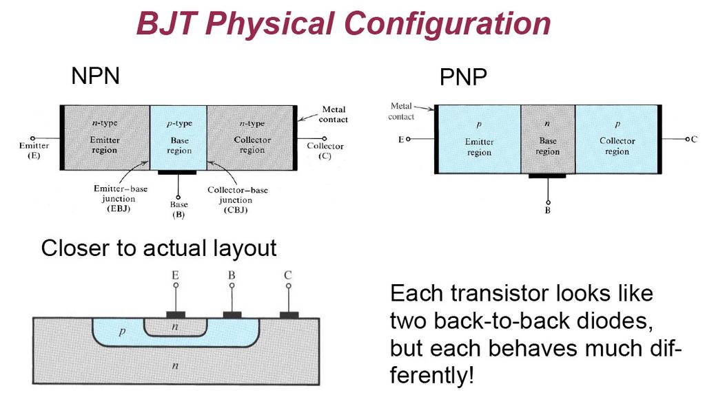
3 Physical Operation of Forward Active NPN BJT i E =i C i B Forward Active => i C = F i E i C = F i B 3
4 Saturation forwardactive 4
5 ESE 319 MT Review cont. 1)Physical operation of a BJT (layout, why currents are related, npn vs. pnp). 2)--> Cover the Eber's Mole Model for forward and reverse active configurations. (large signal model) 3)Cover the various resistances in the small signal model e.g. r(e), r(pi), r(o) etc. 4)Design of PNP transistor circuits. 5)Consider the gain formulae, should we use the -Rc/Re approximation for a CE amplifier, or should we work with the small signal model and consider all the other resistances in parallel. (approximations) 6)CC & CB Amplifier Configurations 5


6 i C i B R F i E i DE i DC I SC I SE 6

7 Ebers-Moll Mode in Forward-Active Mode. 1 i C =I S e v B E V T I S 1 R 1 i E = I v BE S V e T I S 1 1 F F V BE > 0 V BC < 0 i B = 1 F F I S e v BE V T 1 1 R R I S = 1 F e v BE V T I S 1 F 1 R 7
8 Conclusions Ebers-Moll model is accurate large signal model. Used for all operation modes. includes bias + ac. Too complex for pencil-and-paper computations for most applications, e.g. nonlinear. Has been used in computer simulation, e.g. SPICE. 8
9 ESE 319 MT Review cont. 1)Physical operation of a BJT (layout, why currents are related, npn vs. pnp). 2)Cover the Eber's Mole Model for forward and reverse active configurations. (large signal model) 3)--> Cover the various resistances in the small signal model e.g. r(e), r(pi), r(o) etc. 4)Design of PNP transistor circuits. 5)Consider the gain formulae, should we use the -Rc/Re approximation for a CE amplifier, or should we work with the small signal model and consider all the other resistances in parallel. (approximations) 6)CC & CB Amplifier Configurations 9
10 Small Signal Analysis Origin of r π, r e & r o I C VCCS 10
11 Origin of r π, r e & r o cont. r e r e = r 1 Note: i e = 1 i b = 1 v be r = v be r e 11
12 Origin of r π, r e & r o cont. 12
13 Conclusions Resistors g m, r π, r e, r o are equivalent circuit model parameters, not parasitic resistances. Resistor r x, the ohmic base resistance, is a parasitic resistance. v BE V I S e term T from Ebers-Moll model linearized by limiting the ac signal amplitude. 13
14 ESE 319 MT Review cont. 1)Physical operation of a BJT (layout, why currents are related, npn vs. pnp). 2)Cover the Eber's Mole Model for forward and reverse active configurations. (large signal model) 3)Cover the various resistances in the small signal model e.g. r(e), r(pi), r(o) etc. 4)--> Design of PNP transistor circuits. 5)Consider the gain formulae, should we use the -Rc/Re approximation for a CE amplifier, or should we work with the small signal model and consider all the other resistances in parallel. (approximations) 6)CC & CB Amplifier Configurations 14
15 Amplifier Design with PNP Transistors Bipolar process are optimized for NPN performance: a. PNP have lower β than NPN transistors. b. PNP have lower f T than NPN transistors. Example: Intersil CA3096 NPN & PNP array (Data Sheet) NPN: h fe = β = 390, f T = 280 Mhz (I C = 1mA) PNP: h fe = β = 47, f T < 10 Mhz (I C = 1mA) c. NPN transistors are typically used where high gain and f T are needed, e.g. amplifier transistor d. PNP transistors are used where gain and f T are not as needed, e.g. current sources and active loads. e. When NPNs and PNPs are used together, two power supplies are needed. 15
16 NPN vs. PNP CE Design I C I C NPN PNP I I B B IE I E v O Forward Active: V BE 0V V BC 0V Forward Active: V EB 0V V CB 0V 16
17 NPN and PNP Small Signal Models v O v O NPN: dc and ac currents in same direction Small signal model is identical for NPN and PNP transistors! PNP: dc and ac currents in opposite direction due to vsig polarity 17
18 NPN vs. PNP CE Design cont. I 1 I Let C I 1 Let =100 =100 v O I C v O I B I E I B I E V B = R 2 R 2 R 1 V CC R B =R 1 R 2 V B = R 2 R 2 R 1 V CC 0 R B =R 1 R 2 I C = V CC V C R C I C = I B = V V B BE R B 1 R E V E =V B V BE =I E R E I C = V C V CC = V C V CC => V C < 0 R C R C I C = I B = V B V EB R B 1 R E V E =V EB V B =I E R E 0 18
19 Base DC Thevenin Equivalent Circuit I B I C v O => I E V B =I B R B V EB I E R E = R B 1 R E I B V EB V B V EB I B = R B 1 R E I C = I B = V B V EB R B 1 R E 19
20 NPN vs. PNP CE Design Conclusions DC Bias design same for both NPN & PNP. Be careful! PNP DC I & V are inverse of NPN DC I & V. PNP DC supply voltage V CC polarity is inverse of NPN. AC design the same for both NPN & PNP. Small signal models are identical. Be careful! PNP ac current directions are inverse of DC current directions. 20
21 ESE 319 MT Review cont. 1)Physical operation of a BJT (layout, why currents are related, npn vs. pnp). 2)Cover the Eber's Mole Model for forward and reverse active configurations. (large signal model) 3)Cover the various resistances in the small signal model e.g. r(e), r(pi), r(o) etc. 4)Design of PNP transistor circuits. 5)--> Consider the gain formulae, should we use the -Rc/Re approximation for a CE amplifier, or should we work with the small signal model and consider all the other resistances in parallel. (approximations) 6)CC & CB Amplifier Configurations 21
22 Rs 50 Ohm AC Small-Signal CE Voltage Gain b c R S e v c = v o R S v o = R C i c = R S R C v R S r 1 R s E If 1 R S v o R C 1 R E R S A v = v o R C R E 22
23 I REF I REF 23
24 Conclusions Approximations are encouraged when conditions are satisfied, i.e. If R E = 0: v o = R C i c = R C R S r 1 R E => A v = v o R C R E If r π >> R S => A V = v o r R C = g m R C 24
25 ESE 319 MT Review cont. 1)Physical operation of a BJT (layout, why currents are related, npn vs. pnp). 2)Cover the Eber's Mole Model for forward and reverse active configurations. (large signal model) 3)Cover the various resistances in the small signal model e.g. r(e), r(pi), r(o) etc. 4)Design of PNP transistor circuits. 5)Consider the gain formulae, should we use the -Rc/Re approximation for a CE amplifier, or should we work with the small signal model and consider all the other resistances in parallel. (approximations) 6)--> CC & CB Amplifier Configurations 25
26 CC Amplifier R in R out R in R out 26
27 CB Amplifier v O v O R in R out R in R out 27
28 Conclusions low (r e R E ) low (r e ) high (R C r o ) **All parameters for ac small signal. 28
ESE319 Introduction to Microelectronics BJT Intro and Large Signal Model
 BJT Intro and Large Signal Model 1 VLSI Chip Manufacturing Process 2 0.35 mm SiGe BiCMOS Layout for RF (3.5 GHz) Two-Stage Power Amplifier Each transistor above is realized as net of four heterojunction
ECE321 Electronics I Fall 2006
 ECE321 Electronics I Fall 2006 Professor James E. Morris Lecture 11 31 st October, 2006 Bipolar Junction Transistors (BJTs) 5.1 Device Structure & Physics 5.2 I-V Characteristics Convert 5.1 information
CHAPTER 3: BIPOLAR JUNCION TRANSISTOR DR. PHẠM NGUYỄN THANH LOAN
 CHAPTER 3: BIPOLAR JUNCION TRANSISTOR DR. PHẠM NGUYỄN THANH LOAN Hanoi, 9/24/2012 Contents 2 Structure and operation of BJT Different configurations of BJT Characteristic curves DC biasing method and analysis
Electronic Circuits EE359A
 Electronic Circuits EE359A Bruce McNair B206 bmcnair@stevens.edu 201-216-5549 Lecture 4 0 Bipolar Junction Transistors (BJT) Small Signal Analysis Graphical Analysis / Biasing Amplifier, Switch and Logic
Experiment 9 Bipolar Junction Transistor Characteristics
 Experiment 9 Bipolar Junction Transistor Characteristics W.T. Yeung, W.Y. Leung, and R.T. Howe UC Berkeley EE 105 Fall 2005 1.0 Objective In this lab, you will determine the I C - V CE characteristics
I C I E =I B = I C 1 V BE 0.7 V
 Guide to NPN Amplifier Analysis Jason Woytowich 1. Transistor characteristics A BJT has three operating modes cutoff, active, and saturation. For applications, like amplifiers, where linear characteristics
Physics of Bipolar Transistor
 Physics of Bipolar Transistor Motivations - In many electronic applications, amplifier is the most fundamental building block. Ex Audio amplifier: amplifies electric signal to drive a speaker RF Power
Bipolar Junction Transistors (BJTs)
") C H A P T E R 6 Bipolar Junction Transistors (BJTs) Figure 6.1 A simplified structure of the npn transistor and pnp transistor. Table 6.1: BJT modes of Operation Mode Cutoff Active Saturation EBJ Reverse
C H A P T E R 6 Bipolar Junction Transistors (BJTs) Figure 6.1 A simplified structure of the npn transistor and pnp transistor. Table 6.1: BJT modes of Operation Mode Cutoff Active Saturation EBJ Reverse
Lecture 24: Bipolar Junction Transistors (1) Bipolar Junction Structure, Operating Regions, Biasing
 Bipolar Junction Structure, Operating Regions, Biasing") Lecture 24: Bipolar Junction Transistors (1) Bipolar Junction Structure, Operating Regions, Biasing BJT Structure the BJT is formed by doping three semiconductor regions (emitter, base, and collector)
Lecture 24: Bipolar Junction Transistors (1) Bipolar Junction Structure, Operating Regions, Biasing BJT Structure the BJT is formed by doping three semiconductor regions (emitter, base, and collector)
The Bipolar Junction Transistor- Small Signal Characteristics
 The Bipolar Junction Transistor- Small Signal Characteristics Debapratim Ghosh deba21pratim@gmail.com Electronic Systems Group Department of Electrical Engineering Indian Institute of Technology Bombay
EXPERIMENT 12: SIMULATION STUDY OF DIFFERENT BIASING CIRCUITS USING NPN BJT
 EXPERIMENT 12: SIMULATION STUDY OF DIFFERENT BIASING CIRCUITS USING NPN BJT AIM: 1) To study different BJT DC biasing circuits 2) To design voltage divider bias circuit using NPN BJT SOFTWARE TOOL: PC
Electronics EECE2412 Spring 2017 Exam #2
 Electronics EECE2412 Spring 2017 Exam #2 Prof. Charles A. DiMarzio Department of Electrical and Computer Engineering Northeastern University 30 March 2017 File:12198/exams/exam2 Name: : General Rules:
EXPERIMENT 5 CURRENT AND VOLTAGE CHARACTERISTICS OF BJT
 EXPERIMENT 5 CURRENT AND VOLTAGE CHARACTERISTICS OF BJT 1. OBJECTIVES 1.1 To practice how to test NPN and PNP transistors using multimeter. 1.2 To demonstrate the relationship between collector current
Bipolar Junction Transistors (BJTs) Overview
 Overview") 1 Bipolar Junction Transistors (BJTs) Asst. Prof. MONTREE SIRIPRUCHYANUN, D. Eng. Dept. of Teacher Training in Electrical Engineering, Faculty of Technical Education King Mongkut s Institute of Technology
1 Bipolar Junction Transistors (BJTs) Asst. Prof. MONTREE SIRIPRUCHYANUN, D. Eng. Dept. of Teacher Training in Electrical Engineering, Faculty of Technical Education King Mongkut s Institute of Technology
C H A P T E R 6 Bipolar Junction Transistors (BJTs)
") C H A P T E R 6 Bipolar Junction Transistors (BJTs) Figure 6.1 A simplified structure of the npn transistor and pnp transistor. Table 6.1: BJT modes of Operation Mode EBJ CBJ Cutoff Reverse Reverse Active
C H A P T E R 6 Bipolar Junction Transistors (BJTs) Figure 6.1 A simplified structure of the npn transistor and pnp transistor. Table 6.1: BJT modes of Operation Mode EBJ CBJ Cutoff Reverse Reverse Active
Improving Amplifier Voltage Gain
 15.1 Multistage ac-coupled Amplifiers 1077 TABLE 15.3 Three-Stage Amplifier Summary HAND ANALYSIS SPICE RESULTS Voltage gain 998 1010 Input signal range 92.7 V Input resistance 1 M 1M Output resistance
Lecture 12. Bipolar Junction Transistor (BJT) BJT 1-1
 BJT 1-1") Lecture 12 Bipolar Junction Transistor (BJT) BJT 1-1 Course Info Lecture hours: 4 Two Lectures weekly (Saturdays and Wednesdays) Location: K2 Time: 1:40 pm Tutorial hours: 2 One tutorial class every week
Lecture 12 Bipolar Junction Transistor (BJT) BJT 1-1 Course Info Lecture hours: 4 Two Lectures weekly (Saturdays and Wednesdays) Location: K2 Time: 1:40 pm Tutorial hours: 2 One tutorial class every week
Lecture #4 BJT AC Analysis
 November 2014 Ahmad El-Banna Integrated Technical Education Cluster At AlAmeeria J-601-1448 Electronic Principals Lecture #4 BJT AC Analysis Instructor: Dr. Ahmad El-Banna Agenda BJT transistor Modeling
Fundamentals of Microelectronics. Bipolar Amplifier
 Bipolar Amplifier Voltage Amplifier Performance Metrics - There are many metrics that are used to evaluate how good an amplifier is (1) (Voltage) Gain= Vout/ Vin. Can be found from small-signal 10 8 6
Tutorial 2 BJTs, Transistor Bias Circuits, BJT Amplifiers FETs and FETs Amplifiers. Part 1: BJTs, Transistor Bias Circuits and BJT Amplifiers
 Tutorial 2 BJTs, Transistor Bias Circuits, BJT Amplifiers FETs and FETs Amplifiers Part 1: BJTs, Transistor Bias Circuits and BJT Amplifiers 1. Explain the purpose of a thin, lightly doped base region.
Well we know that the battery Vcc must be 9V, so that is taken care of.
 HW 4 For the following problems assume a 9Volt battery available. 1. (50 points, BJT CE design) a) Design a common emitter amplifier using a 2N3904 transistor for a voltage gain of Av=-10 with the collector
ESE319 Introduction to Microelectronics High Frequency BJT Model & Cascode BJT Amplifier
 High Frequency BJT Model & Cascode BJT Amplifier 1 Gain of 10 Amplifier Non-ideal Transistor C in R 1 V CC R 2 v s Gain starts dropping at > 1MHz. Why! Because of internal transistor capacitances that
ECE 310 Microelectronics Circuits
 ECE 310 Microelectronics Circuits Bipolar Transistors Dr. Vishal Saxena (vishalsaxena@boisetstate.edu) Jan 20, 2014 Vishal Saxena 1 Bipolar Transistor n the chapter, we will study the physics of bipolar
Transistor Biasing. DC Biasing of BJT. Transistor Biasing. Transistor Biasing 11/23/2018
 Transistor Biasing DC Biasing of BJT Satish Chandra Assistant Professor Department of Physics P P N College, Kanpur www.satish0402.weebly.com A transistors steady state of operation depends a great deal
ECE 334: Electronic Circuits Lecture 2: BJT Large Signal Model
 Faculty of Engineering ECE 334: Electronic Circuits Lecture 2: BJT Large Signal Model Agenda I & V Notations BJT Devices & Symbols BJT Large Signal Model 2 I, V Notations (1) It is critical to understand
Chapter 6: Transistors and Gain
 I. Introduction Chapter 6: Transistors and Gain This week we introduce the transistor. Transistors are three-terminal devices that can amplify a signal and increase the signal s power. The price is that
Bipolar Junction Transistors
 Bipolar Junction Transistors Invented in 1948 at Bell Telephone laboratories Bipolar junction transistor (BJT) - one of the major three terminal devices Three terminal devices more useful than two terminal
Multistage Amplifiers
 Multistage Amplifiers Single-stage transistor amplifiers are inadequate for meeting most design requirements for any of the four amplifier types (voltage, current, transconductance, and transresistance.)
Chapter 3. Bipolar Junction Transistors
 Chapter 3. Bipolar Junction Transistors Outline: Fundamental of Transistor Common-Base Configuration Common-Emitter Configuration Common-Collector Configuration Introduction The transistor is a three-layer
5.25Chapter V Problem Set
 5.25Chapter V Problem Set P5.1 Analyze the circuits in Fig. P5.1 and determine the base, collector, and emitter currents of the BJTs as well as the voltages at the base, collector, and emitter terminals.
PHYS225 Lecture 6. Electronic Circuits
 PHYS225 Lecture 6 Electronic Circuits Transistors History Basic physics of operation Ebers-Moll model Small signal equivalent Last lecture Introduction to Transistors A transistor is a device with three
Analog Electronics. Electronic Devices, 9th edition Thomas L. Floyd Pearson Education. Upper Saddle River, NJ, All rights reserved.
 Analog Electronics BJT Structure The BJT has three regions called the emitter, base, and collector. Between the regions are junctions as indicated. The base is a thin lightly doped region compared to the
Electronics EECE2412 Spring 2018 Exam #2
 Electronics EECE2412 Spring 2018 Exam #2 Prof. Charles A. DiMarzio Department of Electrical and Computer Engineering Northeastern University 29 March 2018 File:12262/exams/exam2 Name: General Rules: You
4.1.3 Structure of Actual Transistors
 4.1.3 Structure of Actual Transistors Figure 4.7 shows a more realistic BJT cross-section Collector virtually surrounds entire emitter region This makes it difficult for electrons injected into base to
REVIEW TRANSISTOR BIAS CIRCUIT
 EVIEW TANSISTO BIAS CICUIT OBJECTIVES Discuss the concept of dc biasing of a transistor for linear operation Analyze voltage-divider bias, base bias, and collectorfeedback bias circuits. Basic troubleshooting
Experiment #8: Designing and Measuring a Common-Collector Amplifier
 SCHOOL OF ENGINEERING AND APPLIED SCIENCE DEPARTMENT OF ELECTRICAL AND COMPUTER ENGINEERING ECE 2115: ENGINEERING ELECTRONICS LABORATORY Experiment #8: Designing and Measuring a Common-Collector Amplifier
output passes full first (positive) hump and 1/2-scale second hump
 hump and 1/2-scale second hump") 3. For V i > 0, V o 0. For V i < 0, V o V i. The resulting waveform consists only of the negative "humps" of the original cosine wave. Each hump has a duration of 0.5s there is a 0.5s gap between each
3. For V i > 0, V o 0. For V i < 0, V o V i. The resulting waveform consists only of the negative "humps" of the original cosine wave. Each hump has a duration of 0.5s there is a 0.5s gap between each
Chapter 5 Transistor Bias Circuits
 Chapter 5 Transistor Bias Circuits Objectives Discuss the concept of dc biasing of a transistor for linear operation Analyze voltage-divider bias, base bias, and collector-feedback bias circuits. Basic
COE/EE152: Basic Electronics. Lecture 5. Andrew Selasi Agbemenu. Outline
 COE/EE152: Basic Electronics Lecture 5 Andrew Selasi Agbemenu 1 Outline Physical Structure of BJT Two Diode Analogy Modes of Operation Forward Active Mode of BJTs BJT Configurations Early Effect Large
EE105 Fall 2014 Microelectronic Devices and Circuits. NPN Bipolar Junction Transistor (BJT)
") EE105 Fall 2014 Microelectronic Devices and Circuits Prof. Ming C. Wu wu@eecs.berkeley.edu 511 utardja Dai Hall (DH) 1 NPN Bipolar Junction Transistor (BJT) Forward Bias Reverse Bias Hole Flow Electron
EE105 Fall 2014 Microelectronic Devices and Circuits Prof. Ming C. Wu wu@eecs.berkeley.edu 511 utardja Dai Hall (DH) 1 NPN Bipolar Junction Transistor (BJT) Forward Bias Reverse Bias Hole Flow Electron
7. Bipolar Junction Transistor
 41 7. Bipolar Junction Transistor 7.1. Objectives - To experimentally examine the principles of operation of bipolar junction transistor (BJT); - To measure basic characteristics of n-p-n silicon transistor
ECE 255, Discrete-Circuit Amplifiers
 ECE 255, Discrete-Circuit Amplifiers 20 March 2018 In this lecture, we will continue with the study of transistor amplifiers with the presence of biasing circuits and coupling capacitors in place. We will
ET215 Devices I Unit 4A
 ITT Technical Institute ET215 Devices I Unit 4A Chapter 3, Section 3.1-3.2 This unit is divided into two parts; Unit 4A and Unit 4B Chapter 3 Section 3.1 Structure of Bipolar Junction Transistors The basic
Transistors and Applications
 Chapter 17 Transistors and Applications DC Operation of Bipolar Junction Transistors (BJTs) The bipolar junction transistor (BJT) is constructed with three doped semiconductor regions separated by two
F7 Transistor Amplifiers
 Lars Ohlsson 2018-09-25 F7 Transistor Amplifiers Outline Transfer characteristics Small signal operation and models Basic configurations Common source (CS) CS/CE w/ source/ emitter degeneration resistance
Communication Microelectronics (W17)
") Communication Microelectronics (W17) Lecture 4: Bipolar Junction Transistor Assistant Professor Office: C3.315 E-mail: eman.azab@guc.edu.eg 1 Bipolar Junction Transistor (BJT) Physical Structure and I-V
Communication Microelectronics (W17) Lecture 4: Bipolar Junction Transistor Assistant Professor Office: C3.315 E-mail: eman.azab@guc.edu.eg 1 Bipolar Junction Transistor (BJT) Physical Structure and I-V
Lecture 7. ANNOUNCEMENTS MIDTERM #1 willbe held in class on Thursday, October 11 Review session will be held on Friday, October 5
 Lecture 7 ANNOUNCEMENTS MIDTERM #1 willbe held in class on Thursday, October 11 Review session will be held on Friday, October 5 MIDTERM #2 will be held in class on Tuesday, November 13 OUTLINE BJT Amplifiers
Capacitors, diodes, transistors
 Capacitors, diodes, transistors capacitors charging and time response filters (impedance) semi-conductor diodes rectifiers transformers transistors CHM6158C - Lecture 3 1 Capacitors Symbol 2 Capacitors
Chapter 3-2 Semiconductor devices Transistors and Amplifiers-BJT Department of Mechanical Engineering
 MEMS1082 Chapter 3-2 Semiconductor devices Transistors and Amplifiers-BJT Bipolar Transistor Construction npn BJT Transistor Structure npn BJT I = I + E C I B V V BE CE = V = V B C V V E E Base-to-emitter
Lab 2: Common Emitter Design: Part 2
 Lab 2: Common Emitter Design: Part 2 ELE 344 University of Rhode Island, Kingston, RI 02881-0805, U.S.A. 1 Linearity in High Gain Amplifiers The common emitter amplifier, shown in figure 1, will provide
Exercises 6.1, 6.2, 6.3 (page 315 on 7 th edition textbook)
") Exercises 6.1, 6.2, 6.3 (page 315 on 7 th edition textbook) Recapitulation and Equivalent Circuit Models Previous slides present first order BJT model. Assumes npn transistor in active mode. Basic relationship
Exercises 6.1, 6.2, 6.3 (page 315 on 7 th edition textbook) Recapitulation and Equivalent Circuit Models Previous slides present first order BJT model. Assumes npn transistor in active mode. Basic relationship
(a) BJT-OPERATING MODES & CONFIGURATIONS
 BJT-OPERATING MODES & CONFIGURATIONS") (a) BJT-OPERATING MODES & CONFIGURATIONS 1. The leakage current I CBO flows in (a) The emitter, base and collector leads (b) The emitter and base leads. (c) The emitter and collector leads. (d) The base
(a) BJT-OPERATING MODES & CONFIGURATIONS 1. The leakage current I CBO flows in (a) The emitter, base and collector leads (b) The emitter and base leads. (c) The emitter and collector leads. (d) The base
The shape of the waveform will be the same, but its level is shifted either upward or downward. The values of the resistor R and capacitor C affect
 Diode as Clamper A clamping circuit is used to place either the positive or negative peak of a signal at a desired level. The dc component is simply added or subtracted to/from the input signal. The clamper
Engineering Spring Homework Assignment 4: BJT Biasing and Small Signal Properties
 Engineering 1620 -- Spring 2011 Homework Assignment 4: BJT Biasing and Small Signal Properties 1.) The circuit below is a common collector amplifier using constant current biasing. (Constant current biasing
Structure of Actual Transistors
 4.1.3. Structure of Actual Transistors Figure 4.7 shows a more realistic BJT cross-section Collector virtually surrounds entire emitter region This makes it difficult for electrons injected into base to
Lecture 9 Transistors
 Lecture 9 Transistors Physics Transistor/transistor logic CMOS logic CA 1947 http://www.extremetech.com/extreme/164301-graphenetransistors-based-on-negative-resistance-could-spell-theend-of-silicon-and-semiconductors
4.2.2 Metal Oxide Semiconductor Field Effect Transistor (MOSFET)
") 4.2.2 Metal Oxide Semiconductor Field Effect Transistor (MOSFET) The Metal Oxide Semitonductor Field Effect Transistor (MOSFET) has two modes of operation, the depletion mode, and the enhancement mode.
4.2.2 Metal Oxide Semiconductor Field Effect Transistor (MOSFET) The Metal Oxide Semitonductor Field Effect Transistor (MOSFET) has two modes of operation, the depletion mode, and the enhancement mode.
BJT. Bipolar Junction Transistor BJT BJT 11/6/2018. Dr. Satish Chandra, Assistant Professor, P P N College, Kanpur 1
 BJT Bipolar Junction Transistor Satish Chandra Assistant Professor Department of Physics P P N College, Kanpur www.satish0402.weebly.com The Bipolar Junction Transistor is a semiconductor device which
Prof. Anyes Taffard. Physics 120/220. Diode Transistor
 Prof. Anyes Taffard Physics 120/220 Diode Transistor Diode One can think of a diode as a device which allows current to flow in only one direction. Anode I F Cathode stripe Diode conducts current in this
DC Bias. Graphical Analysis. Script
 Course: B.Sc. Applied Physical Science (Computer Science) Year & Sem.: Ist Year, Sem - IInd Subject: Electronics Paper No.: V Paper Title: Analog Circuits Lecture No.: 3 Lecture Title: Analog Circuits
ELEC 2210 EXPERIMENT 7 The Bipolar Junction Transistor (BJT)
") ELEC 2210 EXPERIMENT 7 The Bipolar Junction Transistor (BJT) Objectives: The experiments in this laboratory exercise will provide an introduction to the BJT. You will use the Bit Bucket breadboarding system
ELEC 2210 EXPERIMENT 7 The Bipolar Junction Transistor (BJT) Objectives: The experiments in this laboratory exercise will provide an introduction to the BJT. You will use the Bit Bucket breadboarding system
Transistor electronic technologies
 Transistor electronic technologies Bipolar Junction Transistor discrete or integrated circuit discrete = individual component MOS (Metal-Oxide-Silicon) Field Effect Transistor mainly used in integrated
Lecture #3 BJT Transistors & DC Biasing
 November 2014 Ahmad El-Banna Integrated Technical Education Cluster At AlAmeeria J-601-1448 Electronic Principals Lecture #3 BJT Transistors & DC Biasing Instructor: Dr. Ahmad El-Banna Agenda Transistor
Linear electronic. Lecture No. 1
 1 Lecture No. 1 2 3 4 5 Lecture No. 2 6 7 8 9 10 11 Lecture No. 3 12 13 14 Lecture No. 4 Example: find Frequency response analysis for the circuit shown in figure below. Where R S =4kR B1 =8kR B2 =4k R
Chapter 3: Bipolar Junction Transistors
 Chapter 3: Bipolar Junction Transistors Transistor Construction There are two types of transistors: pnp npn pnp The terminals are labeled: E - Emitter B - Base C - Collector npn 2 Transistor Operation
BJT Circuits (MCQs of Moderate Complexity)
") BJT Circuits (MCQs of Moderate Complexity) 1. The current ib through base of a silicon npn transistor is 1+0.1 cos (1000πt) ma. At 300K, the rπ in the small signal model of the transistor is i b B C r
BJT Circuits (MCQs of Moderate Complexity) 1. The current ib through base of a silicon npn transistor is 1+0.1 cos (1000πt) ma. At 300K, the rπ in the small signal model of the transistor is i b B C r
MOS Field-Effect Transistors (MOSFETs)
") 6 MOS Field-Effect Transistors (MOSFETs) A three-terminal device that uses the voltages of the two terminals to control the current flowing in the third terminal. The basis for amplifier design. The basis
6 MOS Field-Effect Transistors (MOSFETs) A three-terminal device that uses the voltages of the two terminals to control the current flowing in the third terminal. The basis for amplifier design. The basis
KOM2751 Analog Electronics :: Dr. Muharrem Mercimek :: YTU - Control and Automation Dept. 1 2 (CONT D - II) DIODE APPLICATIONS
 DIODE APPLICATIONS") KOM2751 Analog Electronics :: Dr. Muharrem Mercimek :: YTU - Control and Automation Dept. 1 2 (CONT D - II) DIODE APPLICATIONS Most of the content is from the textbook: Electronic devices and circuit theory,
KOM2751 Analog Electronics :: Dr. Muharrem Mercimek :: YTU - Control and Automation Dept. 1 2 (CONT D - II) DIODE APPLICATIONS Most of the content is from the textbook: Electronic devices and circuit theory,
ELECTRONICS LAB. PART 3
 ELECTRONICS LAB. PART 3 Yrd. Doç. Dr. Taha İMECİ Arş. Gör. Ezgi YAMAÇ Arş. Gör. Ufuk ŞANVER İSTANBUL COMMERCE UNIVERSITY Contents TRANSISTORS... 2 5.1 INTRODUCTION... 2 5.2 OPERATION OF TRANSISTORS...
Current Mirrors. Basic BJT Current Mirror. Current mirrors are basic building blocks of analog design. Figure shows the basic NPN current mirror.
 Current Mirrors Basic BJT Current Mirror Current mirrors are basic building blocks of analog design. Figure shows the basic NPN current mirror. For its analysis, we assume identical transistors and neglect
ECEN 325 Lab 7: Characterization and DC Biasing of the BJT
 ECEN 325 Lab 7: Characterization and DC Biasing of the BJT 1 Objectives The purpose of this lab is to characterize NPN and PNP bipolar junction transistors (BJT), and to analyze and design DC biasing circuits
BJT Characteristics & Common Emitter Transistor Amplifier
 LAB #07 Objectives 1. To graph the collector characteristics of a transistor. 2. To measure AC and DC voltages in a common-emitter amplifier. Theory BJT A bipolar (junction) transistor (BJT) is a three-terminal
Electronic Circuits ELCT604 (Spring 2018) Lecture 2 BJT Amplifiers
 Lecture 2 BJT Amplifiers") Electronic Circuits ELCT604 (Spring 2018) Lecture 2 BJT Amplifiers Assistant Professor Office: C3.315 E-mail: eman.azab@guc.edu.eg 1 Analog Voltage Amplifiers Circuit Design and Configurations 2 Objective
Electronic Circuits ELCT604 (Spring 2018) Lecture 2 BJT Amplifiers Assistant Professor Office: C3.315 E-mail: eman.azab@guc.edu.eg 1 Analog Voltage Amplifiers Circuit Design and Configurations 2 Objective
Electronic Circuits - Tutorial 07 BJT transistor 1
 Electronic Circuits - Tutorial 07 BJT transistor 1-1 / 20 - T & F # Question 1 A bipolar junction transistor has three terminals. T 2 For operation in the linear or active region, the base-emitter junction
Phy 335, Unit 4 Transistors and transistor circuits (part one)
") Mini-lecture topics (multiple lectures): Phy 335, Unit 4 Transistors and transistor circuits (part one) p-n junctions re-visited How does a bipolar transistor works; analogy with a valve Basic circuit
Mini-lecture topics (multiple lectures): Phy 335, Unit 4 Transistors and transistor circuits (part one) p-n junctions re-visited How does a bipolar transistor works; analogy with a valve Basic circuit
Alexandria University Faculty of Engineering Electrical Engineering Department
 Chapter 10: Alexandria University Faculty of Engineering Electrical Engineering Department ECE 336: Semiconductor Devices Sheet 6 1. A Si pnp BJT with N AE = 5x10 17 / cm 3, N DB = 10 15 /cm 3 and N AC
EBERS Moll Model. Presented by K.Pandiaraj Assistant Professor ECE Department Kalasalingam University
 EBERS Moll Model Presented by K.Pandiaraj Assistant Professor ECE Department Kalasalingam University BJT Device Models The primary function of a model is to predict the behaviour of a device in particular
ES 330 Electronics II Homework # 2 (Fall 2016 Due Wednesday, September 7, 2016)
") Page1 Name ES 330 Electronics II Homework # 2 (Fall 2016 Due Wednesday, September 7, 2016) Problem 1 (15 points) You are given an NMOS amplifier with drain load resistor R D = 20 k. The DC voltage (V RD
Page1 Name ES 330 Electronics II Homework # 2 (Fall 2016 Due Wednesday, September 7, 2016) Problem 1 (15 points) You are given an NMOS amplifier with drain load resistor R D = 20 k. The DC voltage (V RD
Emitter base bias. Collector base bias Active Forward Reverse Saturation forward Forward Cut off Reverse Reverse Inverse Reverse Forward
 SEMICONDUCTOR PHYSICS-2 [Transistor, constructional characteristics, biasing of transistors, transistor configuration, transistor as an amplifier, transistor as a switch, transistor as an oscillator] Transistor
ESE 372 / Spring 2011 / Lecture 19 Common Base Biased by current source
 ESE 372 / Spring 2011 / Lecture 19 Common Base Biased by current source Output from Collector Start with bias DC analysis make sure BJT is in FA, then calculate small signal parameters for AC analysis.
Lecture (06) BJT Amplifiers 3
 BJT Amplifiers 3") Lecture (06) BJT Amplifiers 3 By: Dr. Ahmed ElShafee ١ THE COMMON COLLECTOR AMPLIFIER An emitter follower circuit with voltage divider bias is shown in Figure, the input signal is capacitively coupled
Lecture (06) BJT Amplifiers 3 By: Dr. Ahmed ElShafee ١ THE COMMON COLLECTOR AMPLIFIER An emitter follower circuit with voltage divider bias is shown in Figure, the input signal is capacitively coupled
Electronic Circuits for Mechatronics ELCT 609 Lecture 5: BJT Voltage Amplifiers
 Electronic Circuits for Mechatronics ELCT 609 Lecture 5: BJT Voltage Amplifiers Assistant Professor Office: C3.315 E-mail: eman.azab@guc.edu.eg 1 BJT Modes of Operation Electrical Equations of BJT 2 BJT
Field Effect Transistors
 Field Effect Transistors Purpose In this experiment we introduce field effect transistors (FETs). We will measure the output characteristics of a FET, and then construct a common-source amplifier stage,
UNIT I - TRANSISTOR BIAS STABILITY
 UNIT I - TRANSISTOR BIAS STABILITY OBJECTIVE On the completion of this unit the student will understand NEED OF BIASING CONCEPTS OF LOAD LINE Q-POINT AND ITS STABILIZATION AND COMPENSATION DIFFERENT TYPES
UNIT 3 Transistors JFET
 UNIT 3 Transistors JFET Mosfet Definition of BJT A bipolar junction transistor is a three terminal semiconductor device consisting of two p-n junctions which is able to amplify or magnify a signal. It
By: Dr. Ahmed ElShafee
 Lecture (04) Transistor Bias Circuit 3 BJT Amplifiers 1 By: Dr. Ahmed ElShafee ١ Emitter Feedback Bias If an emitter resistor is added to the base bias circuit in Figure, the result is emitter feedback
Early Effect & BJT Biasing
 Early Effect & BJT Biasing Early Effect DC BJT Behavior DC Biasing the BJT 1 ESE319 Introduction to Microelectronics Early Effect Saturation region Forward-Active region 4 3 Ideal NPN BJT Transfer V Characteristic
Bipolar junction transistors.
 Bipolar junction transistors. Third Semester Course code : 15EECC202 Analog electronic circuits (AEC) Team: Dr. Nalini C Iyer, R.V. Hangal, Sujata N, Prashant A, Sneha Meti AEC Team, Faculty, School of
Index. Small-Signal Models, 14 saturation current, 3, 5 Transistor Cutoff Frequency, 18 transconductance, 16, 22 transit time, 10
 Index A absolute value, 308 additional pole, 271 analog multiplier, 190 B BiCMOS,107 Bode plot, 266 base-emitter voltage, 16, 50 base-emitter voltages, 296 bias current, 111, 124, 133, 137, 166, 185 bipolar
55:041 Electronic Circuits The University of Iowa Fall Exam 1 Solution
 Exam 1 Name: Score /60 Question 1 Short takes. For True/False questions, write T, or F in the right-hand column as appropriate. For other questions, provide answers in the space provided. 1. Tue of false:
Chapter 3 Bipolar Junction Transistors (BJT)
") Chapter 3 Bipolar Junction Transistors (BJT) Transistors In analog circuits, transistors are used in amplifiers and linear regulated power supplies. In digital circuits they function as electrical switches,
Chapter 3 Bipolar Junction Transistors (BJT) Transistors In analog circuits, transistors are used in amplifiers and linear regulated power supplies. In digital circuits they function as electrical switches,
University of Southern C alifornia School Of Engineering Department Of Electrical Engineering
 University of Southern C alifornia School Of Engineering Department Of Electrical Engineering EE 348: Homework Assignment #04 Spring, 2001 (Due 02/27/2001) Choma Problem #16: n monolithic circuits, diodes
Figure1: Basic BJT construction.
 Chapter 4: Bipolar Junction Transistors (BJTs) Bipolar Junction Transistor (BJT) Structure The BJT is constructed with three doped semiconductor regions separated by two pn junctions, as in Figure 1(a).
PHY405F 2009 EXPERIMENT 6 SIMPLE TRANSISTOR CIRCUITS
 PHY405F 2009 EXPERIMENT 6 SIMPLE TRANSISTOR CIRCUITS Due Date (NOTE CHANGE): Thursday, Nov 12 th @ 5 pm; Late penalty in effect! Most active electronic devices are based on the transistor as the fundamental
The Miller Approximation. CE Frequency Response. The exact analysis is worked out on pp of H&S.
 CE Frequency Response The exact analysis is worked out on pp. 639-64 of H&S. The Miller Approximation Therefore, we consider the effect of C µ on the input node only V ---------- out V s = r g π m ------------------
Transistor Biasing Nafees Ahamad
 Transistor Biasing Nafees Ahamad Asstt. Prof., EECE Deptt, DIT University, Dehradun Website: www.eedofdit.weebly.com Introduction The basic function of transistor is to do amplification. (CE connection)
Transistor fundamentals Nafees Ahamad
 Transistor fundamentals Nafees Ahamad Asstt. Prof., EECE Deptt, DIT University, Dehradun Website: www.eedofdit.weebly.com Transistor A transistor consists of two PN junctions formed by sandwiching either
Homework Assignment 05
 Homework Assignment 05 Question (2 points each unless otherwise indicated)(20 points). Estimate the parallel parasitic capacitance of a mh inductor with an SRF of 220 khz. Answer: (2π)(220 0 3 ) = ( 0
MTLE-6120: Advanced Electronic Properties of Materials. Semiconductor transistors for logic and memory. Reading: Kasap
 MTLE-6120: Advanced Electronic Properties of Materials 1 Semiconductor transistors for logic and memory Reading: Kasap 6.6-6.8 Vacuum tube diodes 2 Thermionic emission from cathode Electrons collected
b b Fig. 1 Transistor symbols
 TRANSISTORS Transistors have three terminals which are referred to as emitter (e), base (b) and collector (c). Fig 1 shows the symbols used for the two types of transistors in common use. c c b b e e npn