Chapter Three " BJT Small-Signal Analysis "
|
|
|
- Mervyn Bradford
- 5 years ago
- Views:
Transcription

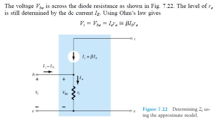
1 Chapter Three " BJT Small-Signal Analysis " We now begin to examine the small-signal ac response of the BJT amplifier by reviewing the models most frequently used to represent the transistor in the sinusoidal ac domain. There are two models commonly used in the small-signal ac analysis of transistor networks: the re model and the hybrid equivalent model. THE re TRANSISTOR MODEL The re model employs a diode and controlled current source to duplicate the behavior of a transistor in the region of interest. In fact, in general: BJT transistor amplifiers are referred to as current-controlled devices. Common Base Configuration: In Fig. 7.16a, a common-base pnp transistor has been inserted within the two-port structure employed in our discussion of the last few sections. In Fig. 7.16b, the re model for the transistor has been placed between the same four terminals. For the base-to-emitter junction of the transistor of Fig. 7.16a, the diode equivalence of Fig. 7.16b between the same two terminals seems to be quite appropriate. The current source of Fig. 7.16b establishes the fact that Ic = αie, with the controlling current Ie appearing in the input side of the equivalent circuit as dictated by Fig. 7.16a. We have therefore established an equivalence at the input and output terminals with the current-controlled source, providing a link between the two an initial review would suggest that the model of Fig. 7.16b is a valid model of the actual device. Recall that the ac resistance of a diode can be determined by the equation r ac = 26 mv/id, where ID is the dc current through the diode at the Q (quiescent) point. This same equation can be used to find the ac resistance of the diode of Fig. 7.16b if we simply substitute the emitter current as follows: 1

2 The subscript e of re was chosen to emphasize that it is the dc level of emitter current that determines the ac level of the resistance of the diode of Fig. 7.16b. Substituting the resulting value of re in Fig. 7.16b will result in the very useful model of Fig Due to the isolation that exists between input and output circuits of Fig. 7.17, it should be fairly obvious that the input impedance Zi for the common-base configuration of a transistor is simply re. That is, For the common-base configuration, typical values of Zi range from a few ohms to a maximum of about 50. For the output impedance, if we set the signal to zero, then Ie = 0 A and Ic = αie = α(0 A) = 0 A, resulting in an open-circuit equivalence at the output terminals. The result is that for the model of Fig. 7.17, In actuality: For the common-base configuration, typical values of Zo are in the megohm range. The output resistance of the common-base configuration is determined by the slope of the characteristic lines of the output characteristics as shown in Fig Assuming the lines to be perfectly horizontal (an excellent approximation) would result in the conclusion of Eq. (7.13). If care were taken to measure Zo graphically or experimentally, levels typically in the range 1- to 2-M would be obtained. 2
3 In general, for the common-base configuration the input impedance is relatively small and the output impedance quite high. The voltage gain will now be determined for the network of Fig

4 For an npn transistor in,the common-base configuration, the equivalence would appear as shown in Fig EXAMPLE:- 4

5 Common Emitter Configuration For the common-emitter configuration of Fig. 7.21a, the input terminals are the base and emitter terminals, but the output set is now the collector and emitter terminals. In addition, the emitter terminal is now common between the input and output ports of the amplifier. Substituting the re equivalent circuit for the npn transistor will result in the configuration of Fig. 7.21b. In this configuration, the base current is the input current while the output current is still Ic. Recall from previouse lectures that the base and collector currents are related by the following equation: 5
6 6
7 For the output impedance, the characteristics of interest are the output set of Fig Note that the slope of the curves increases with increase in collector current. The steeper the slope, the less the level of output impedance (Zo). The re model of Fig does not include an output impedance, but if available from a graphical analysis or from data sheets, it can be included as shown in Fig


8 For the common-emitter configuration, typical values of Zo are in the range of 40 to 50 k. For the model of Fig. 7.25, if the applied signal is set to zero, the current Ic is 0 A and the output impedance is Of course, if the contribution due to ro is ignored as in the re model, the output impedance is defined by Zo =. The voltage gain for the common-emitter configuration will now be determined for the configuration of Fig using the assumption that Zo =. The effect of including ro will be considered in Chapter 8. For the defined direction of Io and polarity of Vo, 8

9 Using the facts that the input impedance is re, the collector current is Ib, and the output impedance is ro, the equivalent model of Fig can be an effective tool in the analysis to follow. For typical parameter values, the common-emitter configuration can be considered one that has a moderate level of input impedance, a high voltage and current gain, and an output impedance that may have to be included in the network analysis. EXAMPLE:- 9
10 Common Collector Configuration For the common-collector configuration, the model defined for the common-emitter configuration of Fig is normally applied rather than defining a model for the common-collector configuration. THE HYBRID EQUIVALENT MODEL: the re model for a transistor is sensitive to the dc level of operation of the amplifier. The result is an input resistance that will vary with the dc operating point. For the hybrid equivalent model to be described in this section, the parameters are defined at an operating point that may or may not reflect the actual operating conditions of the amplifier. The hybrid parameters as shown in Fig are drawn from the specification sheet for the 2N4400 transistor. The quantities hie, hre, hfe, and hoe of Fig are called the hybrid parameters and are the components of a small-signal equivalent circuit to be described shortly. Our description of the hybrid equivalent model will begin with the general twoport system of Fig The following set of equations (7.23) is only one of a number 10
 in each equation results in a hybrid set of units of measurement for the h-parameters.")
11 of ways in which the four variables of Fig can be related. The parameters relating the four variables are called h-parameters from the word hybrid. The term hybrid was chosen because the mixture of variables (V and I ) in each equation results in a hybrid set of units of measurement for the h-parameters. If we arbitrarily set Vo= 0 (short circuit the output terminals) and solve for h11 in Eq. (7.23a), the following will result: Since it is the ratio of the input voltage to the input current with the output terminals shorted, it is called the short-circuit input-impedance parameter. The subscript 11 of h11 defines the fact that the parameter is determined by a ratio of quantities measured at the input terminals. If Ii is set equal to zero by opening the input leads, the following will result for h12: It has no units since it is a ratio of voltage levels and is called the open-circuit reverse transfer voltage ratio parameter. The subscript 12 of h12 reveals that the parameter is a transfer quantity determined by a ratio of input to output measurements. The first integer of the subscript defines the measured quantity to appear in the numerator; the second integer defines the source of the quantity to appear in the denominator. The term reverse is included because the ratio is an input voltage over an output voltage rather than the reverse ratio typically of interest. If in Eq. (7.23b) Vo is equal to zero by again shorting the output terminals, the following will result for h21: 11

12 It is formally called the short-circuit forward transfer current ratio parameter. The subscript 21 again indicates that it is a transfer parameter with the output quantity in the numerator and the input quantity in the denominator. The last parameter, h22, can be found by again opening the input leads to set I1 = 0 and solving for h22 in Eq. (7.23b): It is called the open-circuit output admittance parameter. The subscript 22 reveals that it is determined by a ratio of output quantities. Since each term of Eq. (7.23a) has the unit volt, let us apply Kirchhoff s voltage law in reverse to find a circuit that fits the equation. Performing this operation will result in the circuit of Fig Since the parameter h11 has the unit ohm, it is represented by a resistor in Fig The quantity h12 is dimensionless and therefore simply appears as a multiplying factor of the feedback term in the input circuit. Since each term of Eq. (7.23b) has the units of current, let us now apply Kirchhoff s current law in reverse to obtain the circuit of Fig Since h22 has the units of admittance, which for the transistor model is conductance, it is represented by the resistor symbol. Keep in mind, however, that the resistance in ohms of this resistor is equal to the reciprocal of conductance (1/h22). 12


13 The complete ac equivalent circuit for the basic three-terminal linear device is indicated in Fig with a new set of subscripts for the h-parameters. The notation of Fig is of a more practical nature since it relates the h-parameters to the resulting ratio obtained in the last few paragraphs. The choice of letters is obvious from the following listing: The hybrid equivalent network for the common-emitter configuration appears with the standard notation in Fig Note that Ii = Ib, Io = Ic, and through an application of Kirchhoff s current law, Ie = Ib + Ic. The input voltage is now Vbe, with the output voltage Vce. 13


14 For the common-base configuration of Fig. 7.34, Ii = Ie, Io = Ic with Veb = Vi and Vcb = Vo. The networks of Figs and 7.34 are applicable for pnp or npn transistors. In fact, the hybrid equivalent and the re models for each configuration have been repeated in Fig for comparison. 14

15 It should be reasonably clear from Fig. 7.37a that EXAMPLE: 15
16 16
17 BJT small signal ac analysis The transistor models introduced previously will now be used to perform a small signal ac analysis of a number of standard transistor network configurations. COMMON-EMITTER FIXED-BIAS CONFIGURATION the common-emitter fixed-bias network is shown in Fig The small-signal ac analysis begins by removing the dc effects of VCC and replacing the dc blocking capacitors C1 and C2 by short-circuit equivalents, resulting in the network of Fig Substituting the re model for the common-emitter configuration of Fig. 8.2 will result in the network of Fig

18 The next step is to determine β, re, and ro.figure 8.3 clearly reveals that For the majority of situations RB is greater than βre by more than a factor of 10, For Fig. 8.3, when Vi = 0, Ii =0, Ib =0, resulting in an open-circuit equivalence for the current source. The result is the configuration of Fig Av: The resistors ro and RC are in parallel 18
19 Ai: The current gain is determined in the following manner: Applying the current- divider rule to the input and output circuits, Phase Relationship: The negative sign in the resulting equation for Av reveals that a 180 phase shift occurs between the input and output signals, as shown in Fig
20 EXAMPLE: 20
21 EMITTER-FOLLOWER CONFIGURATION When the output is taken from the emitter terminal of the transistor as shown in Fig. 8.17, the network is referred to as an emitter-follower. 21


22 Substituting the re equivalent circuit into the network of Fig will result in the network of Fig Zi: The input impedance is determined in the same manner as described in the preceding section: Zo: The output impedance is best described by first writing the equation for the current Ib: 22
23 If we now construct the network defined by Eq. (8.41), the configuration of Fig will result. Ai: From Fig. 8.18, 23
24 Phase relationship: As revealed by Eq. (8.44) and earlier discussions of this section, Vo and Vi are in phase for the emitter-follower configuration. Effect of ro: Zi: 24
25 EXAMPLE:- 25
26 26

27 COMMON-BASE CONFIGURATION The common-base configuration is characterized as having a relatively low input and a high output impedance and a current gain less than 1. The voltage gain, however, can be quite large. The standard configuration appears in Fig. 8.23, with the commonbase re equivalent model substituted in Fig
28 Phase relationship: The fact that Av is a positive number reveals that Vo and Vi are in phase for the common-base configuration. Effect of ro: For the common-base configuration, ro = 1/hob is typically in the megohm range and sufficiently larger than the parallel resistance RC to permit the approximation roǁrc RC. EXAMPLE:- 28
29 29
BJT AC Analysis CHAPTER OBJECTIVES 5.1 INTRODUCTION 5.2 AMPLIFICATION IN THE AC DOMAIN
 BJT AC Analysis 5 CHAPTER OBJECTIVES Become familiar with the, hybrid, and hybrid p models for the BJT transistor. Learn to use the equivalent model to find the important ac parameters for an amplifier.
Module-1 BJT AC Analysis: The re Transistor Model. Common-Base Configuration
 Module-1 BJT AC Analysis: BJT AC Analysis: BJT AC Analysis: BJT Transistor Modeling, The re transistor model, Common emitter fixed bias, Voltage divider bias, Emitter follower configuration. Darlington
Chapter Two "Bipolar Transistor Circuits"
 Chapter Two "Bipolar Transistor Circuits" 1.TRANSISTOR CONSTRUCTION:- The transistor is a three-layer semiconductor device consisting of either two n- and one p-type layers of material or two p- and one
BJT. Bipolar Junction Transistor BJT BJT 11/6/2018. Dr. Satish Chandra, Assistant Professor, P P N College, Kanpur 1
 BJT Bipolar Junction Transistor Satish Chandra Assistant Professor Department of Physics P P N College, Kanpur www.satish0402.weebly.com The Bipolar Junction Transistor is a semiconductor device which
Module 2. B.Sc. I Electronics. Developed by: Mrs. Neha S. Joshi Asst. Professor Department of Electronics Willingdon College, Sangli
 Module 2 B.Sc. I Electronics Developed by: Mrs. Neha S. Joshi Asst. Professor Department of Electronics Willingdon College, Sangli BIPOLAR JUNCTION TRANSISTOR SCOPE OF THE CHAPTER- This chapter introduces
ECE 334: Electronic Circuits Lecture 2: BJT Large Signal Model
 Faculty of Engineering ECE 334: Electronic Circuits Lecture 2: BJT Large Signal Model Agenda I & V Notations BJT Devices & Symbols BJT Large Signal Model 2 I, V Notations (1) It is critical to understand
SMALL SINGLE LOW FREQUENCY TRANSISTOR AMPLIFIERS
 UNIT VI SMALL SINGLE LOW FREQUENCY TRANSISTOR 6.1 Introduction AMPLIFIERS V-I characteristics of an active device such as BJT are non-linear. The analysis of a non- linear device is complex. Thus to simplify
Part ILectures Bipolar Junction Transistors(BJTs) and Circuits
 and Circuits") University of missan Electronic II, Second year 2015-2016 Part ILectures Bipolar Junction Transistors(BJTs) and Circuits Assistant Lecture: 1 Bipolar Junction Transistors (BJTs) Bipolar Junction Transistors
University of missan Electronic II, Second year 2015-2016 Part ILectures Bipolar Junction Transistors(BJTs) and Circuits Assistant Lecture: 1 Bipolar Junction Transistors (BJTs) Bipolar Junction Transistors
BASIC ELECTRONICS PROF. T.S. NATARAJAN DEPT OF PHYSICS IIT MADRAS
 BASIC ELECTRONICS PROF. T.S. NATARAJAN DEPT OF PHYSICS IIT MADRAS LECTURE-13 Basic Characteristic of an Amplifier Simple Transistor Model, Common Emitter Amplifier Hello everybody! Today in our series
UNIT II MIDBAND ANALYSIS OF SMALL SIGNAL AMPLIFIERS
 UNIT II MIDBAND ANALYSIS OF SMALL SIGNAL AMPLIFIERS CE, CB and CC amplifiers. Method of drawing small-signal equivalent circuit. Midband analysis of various types of single stage amplifiers to obtain gain,
Basic Electronics Prof. Dr. Chitralekha Mahanta Department of Electronics and Communication Engineering Indian Institute of Technology, Guwahati
 Basic Electronics Prof. Dr. Chitralekha Mahanta Department of Electronics and Communication Engineering Indian Institute of Technology, Guwahati Module: 3 Field Effect Transistors Lecture-8 Junction Field
Analog Circuits Prof. Jayanta Mukherjee Department of Electrical Engineering Indian Institute of Technology - Bombay
 Analog Circuits Prof. Jayanta Mukherjee Department of Electrical Engineering Indian Institute of Technology - Bombay Week - 08 Module - 04 BJT DC Circuits Hello, welcome to another module of this course
PHY405F 2009 EXPERIMENT 6 SIMPLE TRANSISTOR CIRCUITS
 PHY405F 2009 EXPERIMENT 6 SIMPLE TRANSISTOR CIRCUITS Due Date (NOTE CHANGE): Thursday, Nov 12 th @ 5 pm; Late penalty in effect! Most active electronic devices are based on the transistor as the fundamental
Electron Devices and Circuits
 Electron Devices and Circuits (EC 8353) Prepared by Mr.R.Suresh, AP/EEE Ms.S.KARKUZHALI,A.P/EEE BJT small signal model Analysis of CE, CB, CC amplifiers- Gain and frequency response MOSFET small signal
Bipolar junction transistors.
 Bipolar junction transistors. Third Semester Course code : 15EECC202 Analog electronic circuits (AEC) Team: Dr. Nalini C Iyer, R.V. Hangal, Sujata N, Prashant A, Sneha Meti AEC Team, Faculty, School of
By: Dr. Ahmed ElShafee
 Lecture (04) Transistor Bias Circuit 3 BJT Amplifiers 1 By: Dr. Ahmed ElShafee ١ Emitter Feedback Bias If an emitter resistor is added to the base bias circuit in Figure, the result is emitter feedback
Emitter base bias. Collector base bias Active Forward Reverse Saturation forward Forward Cut off Reverse Reverse Inverse Reverse Forward
 SEMICONDUCTOR PHYSICS-2 [Transistor, constructional characteristics, biasing of transistors, transistor configuration, transistor as an amplifier, transistor as a switch, transistor as an oscillator] Transistor
STATIC CHARACTERISTICS OF TRANSISTOR
 STAT CHARACTERISTS OF TRANSISTOR OBJECTIVE The purpose of the experiment is to study the characteristics of bipolar transistor in common emitter (CE) configuration. From the characteristic curve it is
Transistors CHAPTER 3.1 INTRODUCTION
 CHAPTER 3 Bipolar Junction Transistors 3. INTRODUCTION During the period 904 947, the vacuum tube was undoubtedly the electronic device of interest and development. In 904, the vacuum-tube diode was introduced
KOM2751 Analog Electronics :: Dr. Muharrem Mercimek :: YTU - Control and Automation Dept. 1 2 (CONT D - II) DIODE APPLICATIONS
 DIODE APPLICATIONS") KOM2751 Analog Electronics :: Dr. Muharrem Mercimek :: YTU - Control and Automation Dept. 1 2 (CONT D - II) DIODE APPLICATIONS Most of the content is from the textbook: Electronic devices and circuit theory,
KOM2751 Analog Electronics :: Dr. Muharrem Mercimek :: YTU - Control and Automation Dept. 1 2 (CONT D - II) DIODE APPLICATIONS Most of the content is from the textbook: Electronic devices and circuit theory,
Transistor Biasing and Operational amplifier fundamentals. OP-amp Fundamentals and its DC characteristics. BJT biasing schemes
 Lab 1 Transistor Biasing and Operational amplifier fundamentals Experiment 1.1 Experiment 1.2 BJT biasing OP-amp Fundamentals and its DC characteristics BJT biasing schemes 1.1 Objective 1. To sketch potential
Lab 4. Transistor as an amplifier, part 2
 Lab 4 Transistor as an amplifier, part 2 INTRODUCTION We continue the bi-polar transistor experiments begun in the preceding experiment. In the common emitter amplifier experiment, you will learn techniques
Lecture 18: Common Emitter Amplifier.
 Whites, EE 320 Lecture 18 Page 1 of 8 Lecture 18: Common Emitter Amplifier. We will now begin the analysis of the three basic types of linear BJT small-signal amplifiers: 1. Common emitter (CE) 2. Common
e-tutorial Semester I UNIT III and IV
 e-tutorial B. Sc. Electronics Semester-I (Choice Based Credit System) Semester I ELECTRONICS-DSC 1A: NETWORK ANALYSIS AND ANALOG ELECTRONICS UNIT III and IV Sections covered: Bipolar Junction Transistor
DC Bias. Graphical Analysis. Script
 Course: B.Sc. Applied Physical Science (Computer Science) Year & Sem.: Ist Year, Sem - IInd Subject: Electronics Paper No.: V Paper Title: Analog Circuits Lecture No.: 3 Lecture Title: Analog Circuits
BJT h-parameter (H.16)
") BJT h-parameter (H.16) 20170518 Copyright (c) 2016-2017 Young W. Lim. Permission is granted to copy, distribute and/or modify this document under the terms of the GNU Free Documentation License, Version
BJT h-parameter (H.16) 20170518 Copyright (c) 2016-2017 Young W. Lim. Permission is granted to copy, distribute and/or modify this document under the terms of the GNU Free Documentation License, Version
Small signal ac equivalent circuit of BJT
 UNIT-2 Part A 1. What is an ac load line? [N/D 16] A dc load line gives the relationship between the q-point and the transistor characteristics. When capacitors are included in a CE transistor circuit,
Electronics II Lecture 2(a): Bipolar Junction Transistors
: Bipolar Junction Transistors") Lecture 2(a): Bipolar Junction Transistors A/Lectr. Khalid Shakir Dept. Of Engineering Engineering by Pearson Transistor! Transistor=Transfer+Resistor. When Transistor operates in active region its input
Lecture 2(a): Bipolar Junction Transistors A/Lectr. Khalid Shakir Dept. Of Engineering Engineering by Pearson Transistor! Transistor=Transfer+Resistor. When Transistor operates in active region its input
14. Transistor Characteristics Lab
 1 14. Transistor Characteristics Lab Introduction Transistors are the active component in various devices like amplifiers and oscillators. They are called active devices since transistors are capable of
COE/EE152: Basic Electronics. Lecture 5. Andrew Selasi Agbemenu. Outline
 COE/EE152: Basic Electronics Lecture 5 Andrew Selasi Agbemenu 1 Outline Physical Structure of BJT Two Diode Analogy Modes of Operation Forward Active Mode of BJTs BJT Configurations Early Effect Large
The George Washington University School of Engineering and Applied Science Department of Electrical and Computer Engineering ECE 20 - LAB
 The George Washington University School of Engineering and Applied Science Department of Electrical and Computer Engineering ECE 20 - LAB Experiment # 6 (Part I) Bipolar Junction Transistors Common Emitter
Lecture 19: Available Power. Distortion. Emitter Degeneration. Miller Effect.
 Whites, EE 322 Lecture 19 Page 1 of 11 Lecture 19: Available Power. Distortion. Emitter Degeneration. Miller Effect. While the efficiency of an amplifier, as discussed in the previous lecture, is an important
UNIVERSITY OF NORTH CAROLINA AT CHARLOTTE Department of Electrical and Computer Engineering
 UNIVERSITY OF NORTH CAROLINA AT CHARLOTTE Department of Electrical and Computer Engineering EXPERIMENT 7 BJT AMPLIFIER CONFIGURATIONS AND INPUT/OUTPUT IMPEDANCE OBJECTIVES The purpose of this experiment
Electronics Prof D. C. Dube Department of Physics Indian Institute of Technology, Delhi
 Electronics Prof D. C. Dube Department of Physics Indian Institute of Technology, Delhi Module No. # 04 Feedback in Amplifiers, Feedback Configurations and Multi Stage Amplifiers Lecture No. # 03 Input
Chapter 5 Transistor Bias Circuits
 Chapter 5 Transistor Bias Circuits Objectives Discuss the concept of dc biasing of a transistor for linear operation Analyze voltage-divider bias, base bias, and collector-feedback bias circuits. Basic
UNIT I BIASING OF DISCRETE BJT AND MOSFET PART A
 UNIT I BIASING OF DISCRETE BJT AND MOSFET PART A 1. Why do we choose Q point at the center of the load line? 2. Name the two techniques used in the stability of the q point.explain. 3. Give the expression
After the initial bend, the curves approximate a straight line. The slope or gradient of each line represents the output impedance, for a particular
 BJT Biasing A bipolar junction transistor, (BJT) is very versatile. It can be used in many ways, as an amplifier, a switch or an oscillator and many other uses too. Before an input signal is applied its
Electronic Circuits - Tutorial 07 BJT transistor 1
 Electronic Circuits - Tutorial 07 BJT transistor 1-1 / 20 - T & F # Question 1 A bipolar junction transistor has three terminals. T 2 For operation in the linear or active region, the base-emitter junction
BIPOLAR JUNCTION TRANSISTOR (BJT) NOISE MEASUREMENTS 1
 NOISE MEASUREMENTS 1") 4. BIPOLAR JUNCTION TRANSISTOR (BJT) NOISE MEASUREMENTS 4.1 Object The objective of this experiment is to measure the mean-square equivalent input noise, v 2 ni, and base spreading resistance, r x, of
4. BIPOLAR JUNCTION TRANSISTOR (BJT) NOISE MEASUREMENTS 4.1 Object The objective of this experiment is to measure the mean-square equivalent input noise, v 2 ni, and base spreading resistance, r x, of
DEPARTMENT OF ELECTRONICS AND COMMUNICATION ENGINEERING III SEMESTER EC 6304 ELECTRONIC CIRCUITS I. (Regulations 2013)
") DEPARTMENT OF ELECTRONICS AND COMMUNICATION ENGINEERING III SEMESTER EC 6304 ELECTRONIC CIRCUITS I (Regulations 2013 UNIT-1 Part A 1. What is a Q-point? [N/D 16] The operating point also known as quiescent
DEPARTMENT OF ELECTRONICS AND COMMUNICATION ENGINEERING III SEMESTER EC 6304 ELECTRONIC CIRCUITS I (Regulations 2013 UNIT-1 Part A 1. What is a Q-point? [N/D 16] The operating point also known as quiescent
Early Effect & BJT Biasing
 Early Effect & BJT Biasing Early Effect DC BJT Behavior DC Biasing the BJT 1 ESE319 Introduction to Microelectronics Early Effect Saturation region Forward-Active region 4 3 Ideal NPN BJT Transfer V Characteristic
Chapter 6. BJT Amplifiers
 Basic Electronic Devices and Circuits EE 111 Electrical Engineering Majmaah University 2 nd Semester 1432/1433 H Chapter 6 BJT Amplifiers 1 Introduction The things you learned about biasing a transistor
UNIT II SMALL SIGNAL AMPLIFIER
 UNIT II SMALL SIGNAL AMPLIFIER HYBRID MODEL OF A CIRCUIT: A linear ckt have input and output terminal which can be analyzed by 4- parameters (ie.2 -dimensionless and 2- dimension parameters), then it is
Chapter 3 Bipolar Junction Transistors (BJT)
") Chapter 3 Bipolar Junction Transistors (BJT) Transistors In analog circuits, transistors are used in amplifiers and linear regulated power supplies. In digital circuits they function as electrical switches,
Chapter 3 Bipolar Junction Transistors (BJT) Transistors In analog circuits, transistors are used in amplifiers and linear regulated power supplies. In digital circuits they function as electrical switches,
Electrical, Electronic and Digital Principles (EEDP) Lecture 3. Other BJT Biasing Techniques باسم ممدوح الحلوانى
 Lecture 3. Other BJT Biasing Techniques باسم ممدوح الحلوانى") Electrical, Electronic and Digital Principles (EEDP) Lecture 3 Other BJT Biasing Techniques د. باسم ممدوح الحلوانى Approximate Analysis Voltage-divider Bias Exact Analysis Ri = is the equivalent resistance
Electrical, Electronic and Digital Principles (EEDP) Lecture 3 Other BJT Biasing Techniques د. باسم ممدوح الحلوانى Approximate Analysis Voltage-divider Bias Exact Analysis Ri = is the equivalent resistance
Transistor Biasing. DC Biasing of BJT. Transistor Biasing. Transistor Biasing 11/23/2018
 Transistor Biasing DC Biasing of BJT Satish Chandra Assistant Professor Department of Physics P P N College, Kanpur www.satish0402.weebly.com A transistors steady state of operation depends a great deal
Improving Amplifier Voltage Gain
 15.1 Multistage ac-coupled Amplifiers 1077 TABLE 15.3 Three-Stage Amplifier Summary HAND ANALYSIS SPICE RESULTS Voltage gain 998 1010 Input signal range 92.7 V Input resistance 1 M 1M Output resistance
Figure1: Basic BJT construction.
 Chapter 4: Bipolar Junction Transistors (BJTs) Bipolar Junction Transistor (BJT) Structure The BJT is constructed with three doped semiconductor regions separated by two pn junctions, as in Figure 1(a).
ClassABampDesign. Do not design for an edge. Class B push pull stage. Vdd = - Vee. For Vin < Vbe (Ri + Rin2) / Rin2
 / Rin2") ClassABampDesign Richard Cooper October 17 2016 When the input signal is positive, the NPN transistor Q1 turns ON, the PNP transistor Q2 is OFF, and the output voltage is positive. The NPN transistor (emitter
ClassABampDesign Richard Cooper October 17 2016 When the input signal is positive, the NPN transistor Q1 turns ON, the PNP transistor Q2 is OFF, and the output voltage is positive. The NPN transistor (emitter
Università degli Studi di Roma Tor Vergata Dipartimento di Ingegneria Elettronica. Analogue Electronics. Paolo Colantonio A.A.
 Università degli Studi di Roma Tor Vergata Dipartimento di Ingegneria Elettronica Analogue Electronics Paolo olantonio A.A. 2015-16 ias issues The D bias point is affected by thermal issue due to the active
The Common Emitter Amplifier Circuit
 The Common Emitter Amplifier Circuit In the Bipolar Transistor tutorial, we saw that the most common circuit configuration for an NPN transistor is that of the Common Emitter Amplifier circuit and that
Electrical, Electronic and Digital Principles (EEDP) Lecture 3. Other BJT Biasing Techniques باسم ممدوح الحلوانى
 Lecture 3. Other BJT Biasing Techniques باسم ممدوح الحلوانى") Electrical, Electronic and Digital Principles (EEDP) Lecture 3 Other BJT Biasing Techniques د. باسم ممدوح الحلوانى Approximate Analysis Voltage-divider Bias Exact Analysis Ri = is the equivalent resistance
Electrical, Electronic and Digital Principles (EEDP) Lecture 3 Other BJT Biasing Techniques د. باسم ممدوح الحلوانى Approximate Analysis Voltage-divider Bias Exact Analysis Ri = is the equivalent resistance
Experiments #6. Differential Amplifier
 Experiments #6 Differential Amplifier 1) Objectives: To understand the DC and AC operation of a differential amplifier. To measure DC voltages and currents in differential amplifier. To obtain measured
By: Dr. Ahmed ElShafee
 Lecture (02) Transistor operating point & DC Load line (2), Transistor Bias Circuit 1 By: Dr. Ahmed ElShafee ١ DC Load Line The dc operation can be described graphically using a dc load line. This is a
EEE118: Electronic Devices and Circuits
 EEE118: Electronic Devices and Circuits Lecture XIV James E Green Department of Electronic Engineering University of Sheffield j.e.green@sheffield.ac.uk Review Review Considered several transistor switching
The shape of the waveform will be the same, but its level is shifted either upward or downward. The values of the resistor R and capacitor C affect
 Diode as Clamper A clamping circuit is used to place either the positive or negative peak of a signal at a desired level. The dc component is simply added or subtracted to/from the input signal. The clamper
4.2.2 Metal Oxide Semiconductor Field Effect Transistor (MOSFET)
") 4.2.2 Metal Oxide Semiconductor Field Effect Transistor (MOSFET) The Metal Oxide Semitonductor Field Effect Transistor (MOSFET) has two modes of operation, the depletion mode, and the enhancement mode.
4.2.2 Metal Oxide Semiconductor Field Effect Transistor (MOSFET) The Metal Oxide Semitonductor Field Effect Transistor (MOSFET) has two modes of operation, the depletion mode, and the enhancement mode.
ET215 Devices I Unit 4A
 ITT Technical Institute ET215 Devices I Unit 4A Chapter 3, Section 3.1-3.2 This unit is divided into two parts; Unit 4A and Unit 4B Chapter 3 Section 3.1 Structure of Bipolar Junction Transistors The basic
Lecture (01) Transistor operating point & DC Load line
 Transistor operating point & DC Load line") Lecture (01) Transistor operating point & DC Load line By: Dr. Ahmed ElShafee ١ BJT Characteristic Collector Characteristic Curves B C E ٢ BJT modes of operation Conditions in Cutoff Conditions in Saturation
Lecture (01) Transistor operating point & DC Load line By: Dr. Ahmed ElShafee ١ BJT Characteristic Collector Characteristic Curves B C E ٢ BJT modes of operation Conditions in Cutoff Conditions in Saturation
Capacitors, diodes, transistors
 Capacitors, diodes, transistors capacitors charging and time response filters (impedance) semi-conductor diodes rectifiers transformers transistors CHM6158C - Lecture 3 1 Capacitors Symbol 2 Capacitors
EXPERIMENT #3 TRANSISTOR BIASING
 EXPERIMENT #3 TRANSISTOR BIASING Bias (operating point) for a transistor is established by specifying the quiescent (D.C., no signal) values of collector-emitter voltage V CEQ and collector current I CQ.
Physics 623 Transistor Characteristics and Single Transistor Amplifier Sept. 12, 2017
 Physics 623 Transistor Characteristics and Single Transistor Amplifier Sept. 12, 2017 1 Purpose To measure and understand the common emitter transistor characteristic curves. To use the base current gain
CHAPTER 3: BIPOLAR JUNCION TRANSISTOR DR. PHẠM NGUYỄN THANH LOAN
 CHAPTER 3: BIPOLAR JUNCION TRANSISTOR DR. PHẠM NGUYỄN THANH LOAN Hanoi, 9/24/2012 Contents 2 Structure and operation of BJT Different configurations of BJT Characteristic curves DC biasing method and analysis
Analog and Telecommunication Electronics
 Politecnico di Torino - ICT School Analog and Telecommunication Electronics A3 BJT Amplifiers»Biasing» Output dynamic range» Small signal analysis» Voltage gain» Frequency response 12/03/2012-1 ATLCE -
I C I E =I B = I C 1 V BE 0.7 V
 Guide to NPN Amplifier Analysis Jason Woytowich 1. Transistor characteristics A BJT has three operating modes cutoff, active, and saturation. For applications, like amplifiers, where linear characteristics
ELECTRONIC DEVICES AND CIRCUITS LABORATORY MANUAL FOR II / IV B.E (EEE): I - SEMESTER
: I - SEMESTER") ELECTRONIC DEVICES AND CIRCUITS LABORATORY MANUAL FOR II / IV B.E (EEE): I - SEMESTER DEPT. OF ELECTRICAL AND ELECTRONICS ENGINEERING SIR C.R.REDDY COLLEGE OF ENGINEERING ELURU 534 007 ELECTRONIC DEVICES
ELECTRONIC DEVICES AND CIRCUITS LABORATORY MANUAL FOR II / IV B.E (EEE): I - SEMESTER DEPT. OF ELECTRICAL AND ELECTRONICS ENGINEERING SIR C.R.REDDY COLLEGE OF ENGINEERING ELURU 534 007 ELECTRONIC DEVICES
Electronics Lab. (EE21338)
") Princess Sumaya University for Technology The King Abdullah II School for Engineering Electrical Engineering Department Electronics Lab. (EE21338) Prepared By: Eng. Eyad Al-Kouz October, 2012 Table of
Princess Sumaya University for Technology The King Abdullah II School for Engineering Electrical Engineering Department Electronics Lab. (EE21338) Prepared By: Eng. Eyad Al-Kouz October, 2012 Table of
Analysis Of A Transistor Amplifier Circuit Using H-parameters Ppt
 Analysis Of A Transistor Amplifier Circuit Using H-parameters Ppt Amplifiers: transistors biased in the flat-part of the i-v curves Find Q-point from dc equivalent circuit by using appropriate large-signal
ES330 Laboratory Experiment No. 9 Bipolar Differential Amplifier [Reference: Sedra/Smith (Chapter 9; Section 9.2; pp )]
![ES330 Laboratory Experiment No. 9 Bipolar Differential Amplifier [Reference: Sedra/Smith (Chapter 9; Section 9.2; pp )]](/thumbs/84/89341671.jpg "ES330 Laboratory Experiment No. 9 Bipolar Differential Amplifier [Reference: Sedra/Smith (Chapter 9; Section 9.2; pp )]") ES330 Laboratory Experiment No. 9 Bipolar Differential Amplifier [Reference: Sedra/Smith (Chapter 9; Section 9.2; pp. 614-627)] Objectives: 1. Explore the operation of a bipolar junction transistor differential
ES330 Laboratory Experiment No. 9 Bipolar Differential Amplifier [Reference: Sedra/Smith (Chapter 9; Section 9.2; pp. 614-627)] Objectives: 1. Explore the operation of a bipolar junction transistor differential
Lecture (09) Bipolar Junction Transistor 3
 Bipolar Junction Transistor 3") Lecture (09) Bipolar Junction Transistor 3 By: Dr. Ahmed ElShafee ١ I THE BJT AS AN AMPLIFIER Amplification is the process of linearly increasing the amplitude of an electrical signal and is one of the
Lecture (09) Bipolar Junction Transistor 3 By: Dr. Ahmed ElShafee ١ I THE BJT AS AN AMPLIFIER Amplification is the process of linearly increasing the amplitude of an electrical signal and is one of the
EXPERIMENT NO -9 TRANSITOR COMMON -BASE CONFIGURATION CHARACTERISTICS
 Contents EXPERIMENT NO -9 TRANSITOR COMMON -BASE CONFIGURATION CHARACTERISTICS... 3 EXPERIMENT NO -10. FET CHARACTERISTICS... 8 Experiment # 11 Non-inverting amplifier... 13 Experiment #11(B) Inverting
Experiment No. 9 DESIGN AND CHARACTERISTICS OF COMMON BASE AND COMMON COLLECTOR AMPLIFIERS
 Experiment No. 9 DESIGN AND CHARACTERISTICS OF COMMON BASE AND COMMON COLLECTOR AMPLIFIERS 1. Objective: The objective of this experiment is to explore the basic applications of the bipolar junction transistor
Current Mirrors & Current steering Circuits:
 Current Mirrors & Current steering Circuits: MOS Current Steering Circuits: Once a constant current is generated, it can be replicated to provide DC bias currents for the various amplifier stages in the
Expanded Answer: Transistor Amplifier Problem in January/February 2008 Morseman Column
 Expanded Answer: Transistor Amplifier Problem in January/February 2008 Morseman Column Here s what I asked: This month s problem: Figure 4(a) shows a simple npn transistor amplifier. The transistor has
ANALOG ELECTRONICS (AE)
") ANALOG ELECTRONICS (AE) ABOUT COURSE& MARKS SCHEME: 1 Prepared by: BE-EC Amish J. Tankariya SEMESTER-III SUBJECT- ANALOG ELECTRONICS (AE) GTU Subject Code :- 2130902 2 SYLLABUS: 3 4 1 REFERENCE BOOKS:
ANALOG ELECTRONICS (AE) ABOUT COURSE& MARKS SCHEME: 1 Prepared by: BE-EC Amish J. Tankariya SEMESTER-III SUBJECT- ANALOG ELECTRONICS (AE) GTU Subject Code :- 2130902 2 SYLLABUS: 3 4 1 REFERENCE BOOKS:
5.25Chapter V Problem Set
 5.25Chapter V Problem Set P5.1 Analyze the circuits in Fig. P5.1 and determine the base, collector, and emitter currents of the BJTs as well as the voltages at the base, collector, and emitter terminals.
ECEN 325 Lab 7: Characterization and DC Biasing of the BJT
 ECEN 325 Lab 7: Characterization and DC Biasing of the BJT 1 Objectives The purpose of this lab is to characterize NPN and PNP bipolar junction transistors (BJT), and to analyze and design DC biasing circuits
Electronic Circuits EE359A
 Electronic Circuits EE359A Bruce McNair B206 bmcnair@stevens.edu 201-216-5549 Lecture 4 0 Bipolar Junction Transistors (BJT) Small Signal Analysis Graphical Analysis / Biasing Amplifier, Switch and Logic
ELEC 2210 EXPERIMENT 7 The Bipolar Junction Transistor (BJT)
") ELEC 2210 EXPERIMENT 7 The Bipolar Junction Transistor (BJT) Objectives: The experiments in this laboratory exercise will provide an introduction to the BJT. You will use the Bit Bucket breadboarding system
ELEC 2210 EXPERIMENT 7 The Bipolar Junction Transistor (BJT) Objectives: The experiments in this laboratory exercise will provide an introduction to the BJT. You will use the Bit Bucket breadboarding system
Bipolar Junction Transistors
 Bipolar Junction Transistors Invented in 1948 at Bell Telephone laboratories Bipolar junction transistor (BJT) - one of the major three terminal devices Three terminal devices more useful than two terminal
ECE321 Electronics I Fall 2006
 ECE321 Electronics I Fall 2006 Professor James E. Morris Lecture 11 31 st October, 2006 Bipolar Junction Transistors (BJTs) 5.1 Device Structure & Physics 5.2 I-V Characteristics Convert 5.1 information
Chapter 4 DC Biasing BJTs. BJTs
 hapter 4 D Biasing BJTs BJTs Biasing Biasing: The D voltages applied to a transistor in order to turn it on so that it can amplify the A signal. Operating Point The D input establishes an operating or
UNIT-1 Bipolar Junction Transistors. Text Book:, Microelectronic Circuits 6 ed., by Sedra and Smith, Oxford Press
 UNIT-1 Bipolar Junction Transistors Text Book:, Microelectronic Circuits 6 ed., by Sedra and Smith, Oxford Press Figure 6.1 A simplified structure of the npn transistor. Microelectronic Circuits, Sixth
Experiment 8&9 BJT AMPLIFIER
 Experiment 8&9 BJT AMPLIFIER 1 BJT AS AMPLIFIER 1. Objectiv e: 1- To demonstrate the operation and characteristics of small signals common emitter amplifiers. 2- What do we mean by a linear amplifier and
BJT Circuits (MCQs of Moderate Complexity)
") BJT Circuits (MCQs of Moderate Complexity) 1. The current ib through base of a silicon npn transistor is 1+0.1 cos (1000πt) ma. At 300K, the rπ in the small signal model of the transistor is i b B C r
BJT Circuits (MCQs of Moderate Complexity) 1. The current ib through base of a silicon npn transistor is 1+0.1 cos (1000πt) ma. At 300K, the rπ in the small signal model of the transistor is i b B C r
Experiment No. 6 Output Characteristic of Transistor
 Experiment No. 6 Output Characteristic of Transistor Object: To examine the output characteristic of transistor. Apparatus: 1. Two DC power supply. 2. Three AVOmeters. 3. Transistor 2N2222, Resistor 1
(a) BJT-OPERATING MODES & CONFIGURATIONS
 BJT-OPERATING MODES & CONFIGURATIONS") (a) BJT-OPERATING MODES & CONFIGURATIONS 1. The leakage current I CBO flows in (a) The emitter, base and collector leads (b) The emitter and base leads. (c) The emitter and collector leads. (d) The base
(a) BJT-OPERATING MODES & CONFIGURATIONS 1. The leakage current I CBO flows in (a) The emitter, base and collector leads (b) The emitter and base leads. (c) The emitter and collector leads. (d) The base
EEE225: Analogue and Digital Electronics
 EEE225: Analogue and Digital Electronics Lecture I James E. Green Department of Electronic Engineering University of Sheffield j.e.green@sheffield.ac.uk Introduction This Lecture 1 Introduction Aims &
EC6202-ELECTRONIC DEVICES AND CIRCUITS YEAR/SEM: II/III UNIT 1 TWO MARKS. 1. Define diffusion current.
 EC6202-ELECTRONIC DEVICES AND CIRCUITS YEAR/SEM: II/III UNIT 1 TWO MARKS 1. Define diffusion current. A movement of charge carriers due to the concentration gradient in a semiconductor is called process
F7 Transistor Amplifiers
 Lars Ohlsson 2018-09-25 F7 Transistor Amplifiers Outline Transfer characteristics Small signal operation and models Basic configurations Common source (CS) CS/CE w/ source/ emitter degeneration resistance
Analog Electronics. Electronic Devices, 9th edition Thomas L. Floyd Pearson Education. Upper Saddle River, NJ, All rights reserved.
 Analog Electronics BJT Structure The BJT has three regions called the emitter, base, and collector. Between the regions are junctions as indicated. The base is a thin lightly doped region compared to the
Lab 3: BJT Digital Switch
 Lab 3: BJT Digital Switch Objectives The purpose of this lab is to acquaint you with the basic operation of bipolar junction transistor (BJT) and to demonstrate its functionality in digital switching circuits.
Linear electronic. Lecture No. 1
 1 Lecture No. 1 2 3 4 5 Lecture No. 2 6 7 8 9 10 11 Lecture No. 3 12 13 14 Lecture No. 4 Example: find Frequency response analysis for the circuit shown in figure below. Where R S =4kR B1 =8kR B2 =4k R
Objective: To study and verify the functionality of a) PN junction diode in forward bias. Sl.No. Name Quantity Name Quantity 1 Diode
 PN junction diode in forward bias. Sl.No. Name Quantity Name Quantity 1 Diode") Experiment No: 1 Diode Characteristics Objective: To study and verify the functionality of a) PN junction diode in forward bias Components/ Equipments Required: b) Point-Contact diode in reverse bias Components
Experiment No: 1 Diode Characteristics Objective: To study and verify the functionality of a) PN junction diode in forward bias Components/ Equipments Required: b) Point-Contact diode in reverse bias Components
Electronics Fundamentals BIPOLAR TRANSISTORS. Construction, circuit symbols and biasing examples for NPN and PNP junction transistors.
 IPOLA TANSISTOS onstruction, circuit symbols and biasing examples for NPN and PNP junction transistors Slide 1 xternal bias voltages create an electric field, which pulls electrons (emitted into the base
Microelectronics Circuit Analysis and Design
 Neamen Microelectronics Chapter 6-1 Microelectronics Circuit Analysis and Design Donald A. Neamen Chapter 6 Basic BJT Amplifiers Neamen Microelectronics Chapter 6-2 In this chapter, we will: Understand
7. Bipolar Junction Transistor
 41 7. Bipolar Junction Transistor 7.1. Objectives - To experimentally examine the principles of operation of bipolar junction transistor (BJT); - To measure basic characteristics of n-p-n silicon transistor
Lecture (06) Bipolar Junction Transistor
 Bipolar Junction Transistor") Lecture (06) Bipolar Junction Transistor By: Dr. Ahmed lshafee ١ Agenda BJT structure BJT operation BJT characteristics ٢ BJT structure The BJT is constructed with three doped semiconductor regions One
Lecture (06) Bipolar Junction Transistor By: Dr. Ahmed lshafee ١ Agenda BJT structure BJT operation BJT characteristics ٢ BJT structure The BJT is constructed with three doped semiconductor regions One
fiziks Institute for NET/JRF, GATE, IIT-JAM, M.Sc. Entrance, JEST, TIFR and GRE in Physics
 nstitute for NT/JF, GAT, T-JAM, M.Sc. ntrance, JST, TF and G in Physics 3. ipolar Junction Transistors 3.1 Transistor onstruction Transistor is a three-layer semiconductor device consisting of either two
UNIT I - TRANSISTOR BIAS STABILITY
 UNIT I - TRANSISTOR BIAS STABILITY OBJECTIVE On the completion of this unit the student will understand NEED OF BIASING CONCEPTS OF LOAD LINE Q-POINT AND ITS STABILIZATION AND COMPENSATION DIFFERENT TYPES