Bipolar junction transistors.
|
|
|
- Cora Murphy
- 5 years ago
- Views:
Transcription
1 Bipolar junction transistors. Third Semester Course code : 15EECC202 Analog electronic circuits (AEC) Team: Dr. Nalini C Iyer, R.V. Hangal, Sujata N, Prashant A, Sneha Meti AEC Team, Faculty, School of Electronics Engineering, KLE Tech University, Hubballi
2 Lesson Schedule (07 Hrs) 1. Dependence of ic on the collector voltage-the early effect, the common emitter characteristics 2. DC load line and bias point, base-bias 3. Collector to base bias, voltage divider, comparison of bias circuit, 4. small signal models-(the transfer characteristics) of bipolar transistors, two port modeling of amplifiers. 5. AC analysis of BJT circuits-coupling and bypass capacitor, 6. Common emitter circuit analysis, CE circuit with un-bypassed emitter resistor 7.The amplifier gain, operation as a switch
3 3.1. Device Structure and Physical Operation Figure 3.1. shows simplified structure of BJT. Consists of three semiconductor regions: emitter region (n-type) base region (p-type) collector region (n-type) Type described above is referred to as npn. However, pnp types do exist. Microelectronic circuits, fifth edition, Adel s Sedra and Smith Chapter 3, Page NO :
4 3.1.1 Simplified Structure and Modes of Operation Transistor consists of two pn-junctions: emitter-base junction (EBJ) collector-base junction (CBJ) Operating mode depends on biasing. active mode used for amplification cutoff and saturation modes used for switching.
5 3.1.1 Simplified Structure and Modes of Operation Figure 3.1: A simplified structure of the npn transistor.


6 3.1.1 Simplified Structure and Modes of Operation Table : BJT modes of operation Figure 3.2: A simplified structure of the pnp transistor.

7 Operation of the npn- Transistor in the Active Mode Analog electronics circuits (15EECC2020 Active mode is most important. Two external voltage sources are required for biasing to achieve it. Refer to Figure 3.3. Figure 3.3: Current flow in an npn transistor biased to operate in the active mode. (Reverse current components due to drift of thermally generated minority carriers are not shown.)
8 Current Flow Forward bias on emitter-base junction will cause current to flow. This current has two components: electrons injected from emitter into base holes injected from base into emitter. It will be shown that first (of the two above) is desirable. This is achieved with heavy doping of emitter, light doping of base.
9 Current Flow emitter current (i E ) is current which flows across EBJ Flows out of emitter lead minority carriers in p-type region. These electrons will be injected from emitter into base. Opposite direction. Because base is thin, concentration of excess minority carriers within it will exhibit constant gradient.
10 Straight line represents constant gradient. n p n p0 ( x) concentration of minority carriers a position x (where 0 represents EBJ boundary) n thermal-equilibrium value of minority carrier (electron) concentration in base regionn vbe voltage applied across base-emitter junctionnp 0 V thermal voltage (constant) n T p0 vbe / VT (eq6.1) 0 n e n p p0 p0 p0
11 Current Flow Some diffusing electrons will combine with holes (majority carriers in base). Base is thin, however, and recombination is minimal. Recombination does, however, cause gradient to take slightly curved shape. The straight line is assumed.
12 The Collector Current It is observed that most diffusing electrons will reach boundary of collector-base depletion region. Because collector is more positive than base, these electrons are swept into collector. collector current (i C ) is approximately equal to I n. i C = I n Magnitude of i C is independent of v CB. As long as collector is positive, with respect to base. saturation current (I S ) is inversely proportional to W and directly proportional to area of EBJ. Typically between and A Also referred to as scale current. Analog electronics circuits (15EECC202
13 The Base Current base current (i B ) composed of two components: i b1 due to holes injected from base region into emitter. i b2 due to holes that have to be supplied by external circuit to replace those recombined. common-emitter current gain (β.) is influenced by two factors: width of base region (W) relative doping of base emitter regions (N A /N D ) High Value of β thin base (small W in nano-meters) lightly doped base / heavily doped emitter (small N A /N D )
14 The Emitter Current All current which enters transistor must leave. i E = i C + i B

15 Structure of Actual Transistors Figure 3.6 shows a more realistic BJT cross-section. Collector virtually surrounds entire emitter region. This makes it difficult for electrons injected into base to escape collection. Device is not symmetrical. As such, emitter and collector cannot be interchanged. Device is uni-directional. Figure 3.6: Cross-section of an npn BJT.
16 Two questions must be asked to determine whether BJT is in saturation mode, or not: Is the CBJ forward-biased by more than 0.4V? Is the ratio i C /i B less than β.? Operation in Saturation Mode
17 Circuit Symbols and Conventions Figure 3.13: Voltage polarities and current flow in transistors biased in the active mode.
18 The Collector-Base Reverse Current (I CB0 ) Previously, small reverse current was ignored. This is carried by thermally-generated minority carriers. However, it does deserve to be addressed. The collector-base junction current (I CBO ) is normally in the nano-ampere range. Many times higher than its theoreticallypredicted value.
19 Graphical Representation of Transistor Characteristics Analog electronics circuits (15EECC202 Figure 3.15/16: (left) The i C -v BE characteristic for an npn transistor. (right) Effect of temperature on the i C -v BE characteristic. Voltage polarities and current flow in transistors biased in the active mode.
20 Analog electronics circuits (15EECC202 When operated in active region, practical BJT s show some dependence of collector current on collector voltage. As such, i C -v CE characteristic is not straight Dependence of i C on Collector Voltage The Early Effect Fig. V CE VS I C characteristics

21 Figure 3.18: Large-signal equivalent-circuit models of an npn BJT operating in the active mode in the common-emitter configuration with the output resistance r o included.
22 CE configuration Figure 3.19: Common-emitter characteristics. (a) Basic CE circuit; note that in (b) the horizontal scale is expanded around the origin to show the saturation region in some detail. A much greater expansion of the saturation region is shown in (c).
23 BJT as switch Case 1 : When V i < 0.6 V the transistor is off, switch is open, the transisor is operated in cut off region V 0 = V CE = V CC as I B = 0 Case 2: When V i >> 0.6 V the transistor is ON, switch is closed, the transisor is operated in saturation region V 0 = V CE sat = V CC I C R C = 0.3 V Example 3.3 (Solve)
24 3.4. Applying the BJT in Amplifier Design An amplifier may be designed by transistor and series resistance. However, it is necessary to model the voltage transfer characteristic (VTC) Appropriate biasing is important to ensure linear gain, and appropriate input voltage swing. Small-signal model is employed to model the amp s operation.
25 Fig 3.31 (a)simple BJT amplifier with input and output VCE (b) The voltage transfer characteristics(vtc) of an amplifier
26 Figure 3.32: Biasing the BJT amplifier at a point Q located on the active-mode segment of the VTC.
27 Analog electronics circuits (15EECC202 Figure 3.33 BJT amplifier biased at a point Q, with small signal voltage V BE superimposed on the dc Bias voltage V BE.
28 Three-Basic Configurations
29 The Common-Emitter (CE) Amplifier Of three configurations, the CE amplifier is most widely used. Figure 6.50(a) shows a common-emitter amplifier with biasing arrangement omitted. signal course (v sig ) source resistance (R sig ) input resistance (R in ) gain (A vo ) output resistance (R o ) transconductance (G v )
30 Common-Emitter Amplifier Figure 3.50: (a) Common-Emitter Amplifier fed with a signal v sig from a generator with a resistance R sig
31
32 Summary Depending on the bias condition on its two junctions, the BJT can operate in one of three possible modes: cut-off (both junctions reverse biased) active (the EBJ forward-biased and CBJ reversed) saturation (both junctions forward biased) For amplifier applications, the BJT is operated in the active mode. Switching applications make use of the cutoff and saturation modes. A BJT operating in the active mode provides a collector current i C = I S exp{v BE /V T }. The base current i B = i C /, and emitter current i E = i C + i B.
33 Summary To ensure operation in the active mode, the collector voltage of an npn-transistor must be kept higher than approximately 0.4V below the base voltage. For a pnp-transistor, the collector voltage must be lower than approximately 0.4V above the base voltage. Otherwise, the CBJ becomes forward-biased and the transistor will enter saturation. At a constant collector current, the magnitude of the base emitter voltage decreases by about 2mV for every 1 O C rise in temperature. The BJT will be at the edge of saturation when v CE is reduced to about 0.3V.
34 Summary In the active mode, i C shows a slight dependence on v CE. This phenomenon, known as the Early Effect, is modeled by ascribing a finite output resistance to the BJT: r o = V A /I C where V A is the Early Voltage and I C is the dc collector current without the Early Effect taken into account. The dc analysis of transistor circuits is generally simplified by assuming V BE = 0.7V. To operate as a linear amplifier, the BJT is biased in the active region and the signal v be is kept small (v be << V T ). Bias design seeks to establish a dc collector current that is as independent of as possible.
35 What is biasing Need for biasing What is Stabilization Thermal Runaway Derivation of S ICO Bisaing techniques Fixed biasing Emitter resistor bias Base emitter resistor bias Voltage divider resistor bias Approximate analysis Accurate method Exercise 4.7 and 4.8 Biasing Electronic devices and circuits theory Boylestad and Nashelsky Page No
36 Voltage divider Biasing Approximate analysis V B = R 2 V CC / R 1 + R2 V E = V B V BE I E = V E / R E I CQ = I E as I B = 0 V CE = V CC I C R C I E R E Where I E is emitter current I B is base current I C is collector current R C collector resistor R E emitter resistor R 1 R 2 voltage divider circuit
37 Voltage divider Biasing Accurate (Exact) analysis
38 Contd
39 Contd
40 Contd
41 Contd

42 Two port device and hybrid model For the hybrid equivalent model, the parameters are defined at an operating point. The quantities h fe, h re, h oe, h ie are called hybrid parameters and are the components of a small signal equivalent circuit. The description of the hybrid equivalent model will begin with the general two port system. Electronic devices and circuits theory Boylestad and Nashelsky Page No , , voltage divider circuit
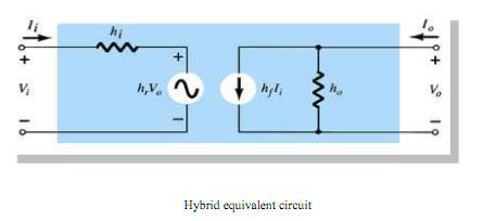
43 Contd

44 Contd Essentially, the transistor model is a three terminal two port system. The h parameters, however, will change with each configuration. To distinguish which parameter has been used or which is available, a second subscript has been added to the h parameter notation

45 Analog electronics circuits (15EECC202 Contd Normally h re is a relatively small quantity, its removal is approximated by hre and hre V 0 = 0 resulting in a short circuit equivalent. The resistance determined by 1/ h oe is often large enough to be ignored in comparison to a parallel load, permitting its replacement by an open circuit equivalent

46 Analog electronics circuits (15EECC202 Analysis of transistor amplifier using h-parameter

47 Contd For analysis of transistor amplifier we have to determine the following terms: Current Gain A I = I 0 / I i = I C / I B Voltage gain Av = V 0 / Vi = - h fe R L / h ie Input impedance Z i = V i / I i = h ie Output impedance Z 0 = V o / I o = 1/ hoe
48 Voltage divider circuit and its equivalent AC Circuit Figure: 1Voltage divider circuit Figure: 2 AC equivalent circuit


49 Voltage divider circuit and its equivalent Approximate h model Figure:3 Equivalent Approximate h model for voltage divider circuit Figure: 4 BJT equivalent h Model
50 Approximate h model Derivation of Z i Z o, A V and A I Input impedance Z i = R 1 R 2 h ie Output impedance Z o = R c Voltage Gain AV= - h fe (R c 1/ h oe ) / h ie Current gain AI = hfe (R 1 R 2 )/ (R 1 R 2 ) + h ie
Microelectronic Circuits, Kyung Hee Univ. Spring, Bipolar Junction Transistors
 Bipolar Junction Transistors 1 Introduction physical structure of the bipolar transistor and how it works How the voltage between two terminals of the transistor controls the current that flows through
Structure of Actual Transistors
 4.1.3. Structure of Actual Transistors Figure 4.7 shows a more realistic BJT cross-section Collector virtually surrounds entire emitter region This makes it difficult for electrons injected into base to
Bipolar Junction Transistors (BJTs) Overview
 Overview") 1 Bipolar Junction Transistors (BJTs) Asst. Prof. MONTREE SIRIPRUCHYANUN, D. Eng. Dept. of Teacher Training in Electrical Engineering, Faculty of Technical Education King Mongkut s Institute of Technology
1 Bipolar Junction Transistors (BJTs) Asst. Prof. MONTREE SIRIPRUCHYANUN, D. Eng. Dept. of Teacher Training in Electrical Engineering, Faculty of Technical Education King Mongkut s Institute of Technology
ECE321 Electronics I Fall 2006
 ECE321 Electronics I Fall 2006 Professor James E. Morris Lecture 11 31 st October, 2006 Bipolar Junction Transistors (BJTs) 5.1 Device Structure & Physics 5.2 I-V Characteristics Convert 5.1 information
4.1.3 Structure of Actual Transistors
 4.1.3 Structure of Actual Transistors Figure 4.7 shows a more realistic BJT cross-section Collector virtually surrounds entire emitter region This makes it difficult for electrons injected into base to
Bipolar Junction Transistors (BJTs)
") C H A P T E R 6 Bipolar Junction Transistors (BJTs) Figure 6.1 A simplified structure of the npn transistor and pnp transistor. Table 6.1: BJT modes of Operation Mode Cutoff Active Saturation EBJ Reverse
C H A P T E R 6 Bipolar Junction Transistors (BJTs) Figure 6.1 A simplified structure of the npn transistor and pnp transistor. Table 6.1: BJT modes of Operation Mode Cutoff Active Saturation EBJ Reverse
Lecture 12. Bipolar Junction Transistor (BJT) BJT 1-1
 BJT 1-1") Lecture 12 Bipolar Junction Transistor (BJT) BJT 1-1 Course Info Lecture hours: 4 Two Lectures weekly (Saturdays and Wednesdays) Location: K2 Time: 1:40 pm Tutorial hours: 2 One tutorial class every week
Lecture 12 Bipolar Junction Transistor (BJT) BJT 1-1 Course Info Lecture hours: 4 Two Lectures weekly (Saturdays and Wednesdays) Location: K2 Time: 1:40 pm Tutorial hours: 2 One tutorial class every week
Bipolar Junction Transistors
 Bipolar Junction Transistors Invented in 1948 at Bell Telephone laboratories Bipolar junction transistor (BJT) - one of the major three terminal devices Three terminal devices more useful than two terminal
COE/EE152: Basic Electronics. Lecture 5. Andrew Selasi Agbemenu. Outline
 COE/EE152: Basic Electronics Lecture 5 Andrew Selasi Agbemenu 1 Outline Physical Structure of BJT Two Diode Analogy Modes of Operation Forward Active Mode of BJTs BJT Configurations Early Effect Large
C H A P T E R 6 Bipolar Junction Transistors (BJTs)
") C H A P T E R 6 Bipolar Junction Transistors (BJTs) Figure 6.1 A simplified structure of the npn transistor and pnp transistor. Table 6.1: BJT modes of Operation Mode EBJ CBJ Cutoff Reverse Reverse Active
C H A P T E R 6 Bipolar Junction Transistors (BJTs) Figure 6.1 A simplified structure of the npn transistor and pnp transistor. Table 6.1: BJT modes of Operation Mode EBJ CBJ Cutoff Reverse Reverse Active
BJT. Bipolar Junction Transistor BJT BJT 11/6/2018. Dr. Satish Chandra, Assistant Professor, P P N College, Kanpur 1
 BJT Bipolar Junction Transistor Satish Chandra Assistant Professor Department of Physics P P N College, Kanpur www.satish0402.weebly.com The Bipolar Junction Transistor is a semiconductor device which
Exercises 6.1, 6.2, 6.3 (page 315 on 7 th edition textbook)
") Exercises 6.1, 6.2, 6.3 (page 315 on 7 th edition textbook) Recapitulation and Equivalent Circuit Models Previous slides present first order BJT model. Assumes npn transistor in active mode. Basic relationship
Exercises 6.1, 6.2, 6.3 (page 315 on 7 th edition textbook) Recapitulation and Equivalent Circuit Models Previous slides present first order BJT model. Assumes npn transistor in active mode. Basic relationship
Analog & Digital Electronics Course No: PH-218
 Analog & Digital Electronics Course No: PH-218 Lec-5: Bipolar Junction Transistor (BJT) Course nstructors: Dr. A. P. VAJPEY Department of Physics, ndian nstitute of Technology Guwahati, ndia 1 Bipolar
Physics of Bipolar Transistor
 Physics of Bipolar Transistor Motivations - In many electronic applications, amplifier is the most fundamental building block. Ex Audio amplifier: amplifies electric signal to drive a speaker RF Power
Chapter Two "Bipolar Transistor Circuits"
 Chapter Two "Bipolar Transistor Circuits" 1.TRANSISTOR CONSTRUCTION:- The transistor is a three-layer semiconductor device consisting of either two n- and one p-type layers of material or two p- and one
Chapter 3 Bipolar Junction Transistors (BJT)
") Chapter 3 Bipolar Junction Transistors (BJT) Transistors In analog circuits, transistors are used in amplifiers and linear regulated power supplies. In digital circuits they function as electrical switches,
Chapter 3 Bipolar Junction Transistors (BJT) Transistors In analog circuits, transistors are used in amplifiers and linear regulated power supplies. In digital circuits they function as electrical switches,
The shape of the waveform will be the same, but its level is shifted either upward or downward. The values of the resistor R and capacitor C affect
 Diode as Clamper A clamping circuit is used to place either the positive or negative peak of a signal at a desired level. The dc component is simply added or subtracted to/from the input signal. The clamper
Lecture 24: Bipolar Junction Transistors (1) Bipolar Junction Structure, Operating Regions, Biasing
 Bipolar Junction Structure, Operating Regions, Biasing") Lecture 24: Bipolar Junction Transistors (1) Bipolar Junction Structure, Operating Regions, Biasing BJT Structure the BJT is formed by doping three semiconductor regions (emitter, base, and collector)
Lecture 24: Bipolar Junction Transistors (1) Bipolar Junction Structure, Operating Regions, Biasing BJT Structure the BJT is formed by doping three semiconductor regions (emitter, base, and collector)
UNIT-1 Bipolar Junction Transistors. Text Book:, Microelectronic Circuits 6 ed., by Sedra and Smith, Oxford Press
 UNIT-1 Bipolar Junction Transistors Text Book:, Microelectronic Circuits 6 ed., by Sedra and Smith, Oxford Press Figure 6.1 A simplified structure of the npn transistor. Microelectronic Circuits, Sixth
KOM2751 Analog Electronics :: Dr. Muharrem Mercimek :: YTU - Control and Automation Dept. 1 2 (CONT D - II) DIODE APPLICATIONS
 DIODE APPLICATIONS") KOM2751 Analog Electronics :: Dr. Muharrem Mercimek :: YTU - Control and Automation Dept. 1 2 (CONT D - II) DIODE APPLICATIONS Most of the content is from the textbook: Electronic devices and circuit theory,
KOM2751 Analog Electronics :: Dr. Muharrem Mercimek :: YTU - Control and Automation Dept. 1 2 (CONT D - II) DIODE APPLICATIONS Most of the content is from the textbook: Electronic devices and circuit theory,
(a) BJT-OPERATING MODES & CONFIGURATIONS
 BJT-OPERATING MODES & CONFIGURATIONS") (a) BJT-OPERATING MODES & CONFIGURATIONS 1. The leakage current I CBO flows in (a) The emitter, base and collector leads (b) The emitter and base leads. (c) The emitter and collector leads. (d) The base
(a) BJT-OPERATING MODES & CONFIGURATIONS 1. The leakage current I CBO flows in (a) The emitter, base and collector leads (b) The emitter and base leads. (c) The emitter and collector leads. (d) The base
An Introduction to Bipolar Junction Transistors. Prepared by Dr Yonas M Gebremichael, 2005
 An Introduction to Bipolar Junction Transistors Transistors Transistors are three port devices used in most integrated circuits such as amplifiers. Non amplifying components we have seen so far, such as
Figure1: Basic BJT construction.
 Chapter 4: Bipolar Junction Transistors (BJTs) Bipolar Junction Transistor (BJT) Structure The BJT is constructed with three doped semiconductor regions separated by two pn junctions, as in Figure 1(a).
UNIT-III Bipolar Junction Transistor
 DC UNT-3.xplain the construction and working of JT. UNT- ipolar Junction Transistor A bipolar (junction) transistor (JT) is a three-terminal electronic device constructed of doped semiconductor material
Electronic Circuits EE359A
 Electronic Circuits EE359A Bruce McNair B206 bmcnair@stevens.edu 201-216-5549 Lecture 4 0 Bipolar Junction Transistors (BJT) Small Signal Analysis Graphical Analysis / Biasing Amplifier, Switch and Logic
ECE 310 Microelectronics Circuits
 ECE 310 Microelectronics Circuits Bipolar Transistors Dr. Vishal Saxena (vishalsaxena@boisetstate.edu) Jan 20, 2014 Vishal Saxena 1 Bipolar Transistor n the chapter, we will study the physics of bipolar
Chapter 3. Bipolar Junction Transistors
 Chapter 3. Bipolar Junction Transistors Outline: Fundamental of Transistor Common-Base Configuration Common-Emitter Configuration Common-Collector Configuration Introduction The transistor is a three-layer
Bipolar Junction Transistor (BJT) Basics- GATE Problems
 Basics- GATE Problems") Bipolar Junction Transistor (BJT) Basics- GATE Problems One Mark Questions 1. The break down voltage of a transistor with its base open is BV CEO and that with emitter open is BV CBO, then (a) BV CEO =
Bipolar Junction Transistor (BJT) Basics- GATE Problems One Mark Questions 1. The break down voltage of a transistor with its base open is BV CEO and that with emitter open is BV CBO, then (a) BV CEO =
MOS Field-Effect Transistors (MOSFETs)
") 6 MOS Field-Effect Transistors (MOSFETs) A three-terminal device that uses the voltages of the two terminals to control the current flowing in the third terminal. The basis for amplifier design. The basis
6 MOS Field-Effect Transistors (MOSFETs) A three-terminal device that uses the voltages of the two terminals to control the current flowing in the third terminal. The basis for amplifier design. The basis
Basic Electronics Prof. Dr. Chitralekha Mahanta Department of Electronics and Communication Engineering Indian Institute of Technology, Guwahati
 Basic Electronics Prof. Dr. Chitralekha Mahanta Department of Electronics and Communication Engineering Indian Institute of Technology, Guwahati Module: 2 Bipolar Junction Transistors Lecture-1 Transistor
ECE 440 Lecture 29 : Introduction to the BJT-I Class Outline:
 ECE 440 Lecture 29 : Introduction to the BJT-I Class Outline: Narrow-Base Diode BJT Fundamentals BJT Amplification Things you should know when you leave Key Questions How does the narrow-base diode multiply
ECE 442 Solid State Devices & Circuits. 6. Bipolar Transistors
 ECE 442 Solid State Devices & Circuits 6. Bipolar Transistors Jose E. Schutt-Aine Electrical & Computer Engineering University of Illinois jschutt@emlab.uiuc.edu ECE 342 Jose Schutt Aine 1 Bipolar Junction
Chapter 3-2 Semiconductor devices Transistors and Amplifiers-BJT Department of Mechanical Engineering
 MEMS1082 Chapter 3-2 Semiconductor devices Transistors and Amplifiers-BJT Bipolar Transistor Construction npn BJT Transistor Structure npn BJT I = I + E C I B V V BE CE = V = V B C V V E E Base-to-emitter
5.1 BJT Device Structure and Physical Operation
 11/28/2004 section 5_1 BJT Device Structure and Physical Operation blank 1/2 5.1 BJT Device Structure and Physical Operation Reading Assignment: pp. 377-392 Another kind of transistor is the Bipolar Junction
Electronic Circuits - Tutorial 07 BJT transistor 1
 Electronic Circuits - Tutorial 07 BJT transistor 1-1 / 20 - T & F # Question 1 A bipolar junction transistor has three terminals. T 2 For operation in the linear or active region, the base-emitter junction
I E I C since I B is very small
 Figure 2: Symbols and nomenclature of a (a) npn and (b) pnp transistor. The BJT consists of three regions, emitter, base, and collector. The emitter and collector are usually of one type of doping, while
Electronics I - Physics of Bipolar Transistors
 Chapter 5 Electronics I - Physics of Bipolar Transistors B E N+ P N- C B E C Fall 2017 claudio talarico 1 source: Sedra & Smith Thin Base Types of Bipolar Transistors n+ p n- Figure - A simplified structure
Lecture 3: Transistors
 Lecture 3: Transistors Now that we know about diodes, let s put two of them together, as follows: collector base emitter n p n moderately doped lightly doped, and very thin heavily doped At first glance,
Chapter Three " BJT Small-Signal Analysis "
 Chapter Three " BJT Small-Signal Analysis " We now begin to examine the small-signal ac response of the BJT amplifier by reviewing the models most frequently used to represent the transistor in the sinusoidal
EE105 Fall 2014 Microelectronic Devices and Circuits. NPN Bipolar Junction Transistor (BJT)
") EE105 Fall 2014 Microelectronic Devices and Circuits Prof. Ming C. Wu wu@eecs.berkeley.edu 511 utardja Dai Hall (DH) 1 NPN Bipolar Junction Transistor (BJT) Forward Bias Reverse Bias Hole Flow Electron
EE105 Fall 2014 Microelectronic Devices and Circuits Prof. Ming C. Wu wu@eecs.berkeley.edu 511 utardja Dai Hall (DH) 1 NPN Bipolar Junction Transistor (BJT) Forward Bias Reverse Bias Hole Flow Electron
EE301 Electronics I , Fall
 EE301 Electronics I 2018-2019, Fall 1. Introduction to Microelectronics (1 Week/3 Hrs.) Introduction, Historical Background, Basic Consepts 2. Rewiev of Semiconductors (1 Week/3 Hrs.) Semiconductor materials
7. Bipolar Junction Transistor
 41 7. Bipolar Junction Transistor 7.1. Objectives - To experimentally examine the principles of operation of bipolar junction transistor (BJT); - To measure basic characteristics of n-p-n silicon transistor
Communication Microelectronics (W17)
") Communication Microelectronics (W17) Lecture 4: Bipolar Junction Transistor Assistant Professor Office: C3.315 E-mail: eman.azab@guc.edu.eg 1 Bipolar Junction Transistor (BJT) Physical Structure and I-V
Communication Microelectronics (W17) Lecture 4: Bipolar Junction Transistor Assistant Professor Office: C3.315 E-mail: eman.azab@guc.edu.eg 1 Bipolar Junction Transistor (BJT) Physical Structure and I-V
Module-1 BJT AC Analysis: The re Transistor Model. Common-Base Configuration
 Module-1 BJT AC Analysis: BJT AC Analysis: BJT AC Analysis: BJT Transistor Modeling, The re transistor model, Common emitter fixed bias, Voltage divider bias, Emitter follower configuration. Darlington
Chapter 3: TRANSISTORS. Dr. Gopika Sood PG Govt. College For Girls Sector -11, Chandigarh
 Chapter 3: TRANSISTORS Dr. Gopika Sood PG Govt. College For Girls Sector -11, Chandigarh OUTLINE Transistors Bipolar Junction Transistor (BJT) Operation of Transistor Transistor parameters Load Line Biasing
ET215 Devices I Unit 4A
 ITT Technical Institute ET215 Devices I Unit 4A Chapter 3, Section 3.1-3.2 This unit is divided into two parts; Unit 4A and Unit 4B Chapter 3 Section 3.1 Structure of Bipolar Junction Transistors The basic
ESE319 Introduction to Microelectronics BJT Intro and Large Signal Model
 BJT Intro and Large Signal Model 1 VLSI Chip Manufacturing Process 2 0.35 mm SiGe BiCMOS Layout for RF (3.5 GHz) Two-Stage Power Amplifier Each transistor above is realized as net of four heterojunction
Transistor Biasing and Operational amplifier fundamentals. OP-amp Fundamentals and its DC characteristics. BJT biasing schemes
 Lab 1 Transistor Biasing and Operational amplifier fundamentals Experiment 1.1 Experiment 1.2 BJT biasing OP-amp Fundamentals and its DC characteristics BJT biasing schemes 1.1 Objective 1. To sketch potential
Alexandria University Faculty of Engineering Electrical Engineering Department
 Chapter 10: Alexandria University Faculty of Engineering Electrical Engineering Department ECE 336: Semiconductor Devices Sheet 6 1. A Si pnp BJT with N AE = 5x10 17 / cm 3, N DB = 10 15 /cm 3 and N AC
Transistors and Applications
 Chapter 17 Transistors and Applications DC Operation of Bipolar Junction Transistors (BJTs) The bipolar junction transistor (BJT) is constructed with three doped semiconductor regions separated by two
Module 2. B.Sc. I Electronics. Developed by: Mrs. Neha S. Joshi Asst. Professor Department of Electronics Willingdon College, Sangli
 Module 2 B.Sc. I Electronics Developed by: Mrs. Neha S. Joshi Asst. Professor Department of Electronics Willingdon College, Sangli BIPOLAR JUNCTION TRANSISTOR SCOPE OF THE CHAPTER- This chapter introduces
EC6202-ELECTRONIC DEVICES AND CIRCUITS YEAR/SEM: II/III UNIT 1 TWO MARKS. 1. Define diffusion current.
 EC6202-ELECTRONIC DEVICES AND CIRCUITS YEAR/SEM: II/III UNIT 1 TWO MARKS 1. Define diffusion current. A movement of charge carriers due to the concentration gradient in a semiconductor is called process
Early Effect & BJT Biasing
 Early Effect & BJT Biasing Early Effect DC BJT Behavior DC Biasing the BJT 1 ESE319 Introduction to Microelectronics Early Effect Saturation region Forward-Active region 4 3 Ideal NPN BJT Transfer V Characteristic
Microelectronics Circuit Analysis and Design
 Neamen Microelectronics Chapter 6-1 Microelectronics Circuit Analysis and Design Donald A. Neamen Chapter 6 Basic BJT Amplifiers Neamen Microelectronics Chapter 6-2 In this chapter, we will: Understand
DC Bias. Graphical Analysis. Script
 Course: B.Sc. Applied Physical Science (Computer Science) Year & Sem.: Ist Year, Sem - IInd Subject: Electronics Paper No.: V Paper Title: Analog Circuits Lecture No.: 3 Lecture Title: Analog Circuits
Analog Electronics. Electronic Devices, 9th edition Thomas L. Floyd Pearson Education. Upper Saddle River, NJ, All rights reserved.
 Analog Electronics BJT Structure The BJT has three regions called the emitter, base, and collector. Between the regions are junctions as indicated. The base is a thin lightly doped region compared to the
ECE 334: Electronic Circuits Lecture 2: BJT Large Signal Model
 Faculty of Engineering ECE 334: Electronic Circuits Lecture 2: BJT Large Signal Model Agenda I & V Notations BJT Devices & Symbols BJT Large Signal Model 2 I, V Notations (1) It is critical to understand
EEE225: Analogue and Digital Electronics
 EEE225: Analogue and Digital Electronics Lecture I James E. Green Department of Electronic Engineering University of Sheffield j.e.green@sheffield.ac.uk Introduction This Lecture 1 Introduction Aims &
CHAPTER 3: BIPOLAR JUNCION TRANSISTOR DR. PHẠM NGUYỄN THANH LOAN
 CHAPTER 3: BIPOLAR JUNCION TRANSISTOR DR. PHẠM NGUYỄN THANH LOAN Hanoi, 9/24/2012 Contents 2 Structure and operation of BJT Different configurations of BJT Characteristic curves DC biasing method and analysis
Bipolar Junction Transistors (BJT)
") Bipolar Junction Transistors (BJT) deal Transistor Bipolar Transistor Terminals P Bipolar Transistor Physics Large Signal Model Early Effect Small Signal Model Reading: (Sedra, Smith, 7 th edition) 4.1
Bipolar Junction Transistors (BJT) deal Transistor Bipolar Transistor Terminals P Bipolar Transistor Physics Large Signal Model Early Effect Small Signal Model Reading: (Sedra, Smith, 7 th edition) 4.1
BJT Amplifier. Superposition principle (linear amplifier)
") BJT Amplifier Two types analysis DC analysis Applied DC voltage source AC analysis Time varying signal source Superposition principle (linear amplifier) The response of a linear amplifier circuit excited
BJT Amplifier Two types analysis DC analysis Applied DC voltage source AC analysis Time varying signal source Superposition principle (linear amplifier) The response of a linear amplifier circuit excited
BJT Circuits (MCQs of Moderate Complexity)
") BJT Circuits (MCQs of Moderate Complexity) 1. The current ib through base of a silicon npn transistor is 1+0.1 cos (1000πt) ma. At 300K, the rπ in the small signal model of the transistor is i b B C r
BJT Circuits (MCQs of Moderate Complexity) 1. The current ib through base of a silicon npn transistor is 1+0.1 cos (1000πt) ma. At 300K, the rπ in the small signal model of the transistor is i b B C r
UNIT 3: FIELD EFFECT TRANSISTORS
 FIELD EFFECT TRANSISTOR: UNIT 3: FIELD EFFECT TRANSISTORS The field effect transistor is a semiconductor device, which depends for its operation on the control of current by an electric field. There are
PHYS225 Lecture 6. Electronic Circuits
 PHYS225 Lecture 6 Electronic Circuits Transistors History Basic physics of operation Ebers-Moll model Small signal equivalent Last lecture Introduction to Transistors A transistor is a device with three
SUMMER 13 EXAMINATION Subject Code: Model Answer Page No: / N
 Important Instructions to examiners: 1) The answers should be examined by key words and not as word-to-word as given in the model answer scheme. 2) The model answer and the answer written by candidate
(Refer Slide Time: 05:47)
") Solid State Devices Dr. S. Karmalkar Department of Electronics and Communication Engineering Indian Institute of Technology, Madras Lecture - 29 Bipolar Junction Transistor (Contd ) So we have been discussing
Solid State Devices Dr. S. Karmalkar Department of Electronics and Communication Engineering Indian Institute of Technology, Madras Lecture - 29 Bipolar Junction Transistor (Contd ) So we have been discussing
Emitter base bias. Collector base bias Active Forward Reverse Saturation forward Forward Cut off Reverse Reverse Inverse Reverse Forward
 SEMICONDUCTOR PHYSICS-2 [Transistor, constructional characteristics, biasing of transistors, transistor configuration, transistor as an amplifier, transistor as a switch, transistor as an oscillator] Transistor
Electron Devices and Circuits
 Electron Devices and Circuits (EC 8353) Prepared by Mr.R.Suresh, AP/EEE Ms.S.KARKUZHALI,A.P/EEE BJT small signal model Analysis of CE, CB, CC amplifiers- Gain and frequency response MOSFET small signal
Transistor Biasing. DC Biasing of BJT. Transistor Biasing. Transistor Biasing 11/23/2018
 Transistor Biasing DC Biasing of BJT Satish Chandra Assistant Professor Department of Physics P P N College, Kanpur www.satish0402.weebly.com A transistors steady state of operation depends a great deal
Part ILectures Bipolar Junction Transistors(BJTs) and Circuits
 and Circuits") University of missan Electronic II, Second year 2015-2016 Part ILectures Bipolar Junction Transistors(BJTs) and Circuits Assistant Lecture: 1 Bipolar Junction Transistors (BJTs) Bipolar Junction Transistors
University of missan Electronic II, Second year 2015-2016 Part ILectures Bipolar Junction Transistors(BJTs) and Circuits Assistant Lecture: 1 Bipolar Junction Transistors (BJTs) Bipolar Junction Transistors
Reg. No. : Question Paper Code : B.E./B.Tech. DEGREE EXAMINATION, NOVEMBER/DECEMBER Second Semester
 WK 5 Reg. No. : Question Paper Code : 27184 B.E./B.Tech. DEGREE EXAMINATION, NOVEMBER/DECEMBER 2015. Time : Three hours Second Semester Electronics and Communication Engineering EC 6201 ELECTRONIC DEVICES
UNIT 3 Transistors JFET
 UNIT 3 Transistors JFET Mosfet Definition of BJT A bipolar junction transistor is a three terminal semiconductor device consisting of two p-n junctions which is able to amplify or magnify a signal. It
Prof. Paolo Colantonio a.a
 Prof. Paolo olantonio a.a. 2011 12 ipolar transistors are one of the main building blocks in electronic systems They are used in both analogue and digital circuits They incorporate two pn junctions and
e-tutorial Semester I UNIT III and IV
 e-tutorial B. Sc. Electronics Semester-I (Choice Based Credit System) Semester I ELECTRONICS-DSC 1A: NETWORK ANALYSIS AND ANALOG ELECTRONICS UNIT III and IV Sections covered: Bipolar Junction Transistor
Student Lecture by: Giangiacomo Groppi Joel Cassell Pierre Berthelot September 28 th 2004
 Student Lecture by: Giangiacomo Groppi Joel Cassell Pierre Berthelot September 28 th 2004 Lecture outline Historical introduction Semiconductor devices overview Bipolar Junction Transistor (BJT) Field
Solid State Devices- Part- II. Module- IV
 Solid State Devices- Part- II Module- IV MOS Capacitor Two terminal MOS device MOS = Metal- Oxide- Semiconductor MOS capacitor - the heart of the MOSFET The MOS capacitor is used to induce charge at the
Shankersinh Vaghela Bapu Institute of Technology INDEX
 Shankersinh Vaghela Bapu Institute of Technology Diploma EE Semester III 3330905: ELECTRONIC COMPONENTS AND CIRCUITS INDEX Sr. No. Title Page Date Sign Grade 1 Obtain I-V characteristic of Diode. 2 To
Transistor Characteristics
 Transistor Characteristics Topics covered in this presentation: Transistor Construction Transistor Operation Transistor Characteristics 1 of 15 The Transistor The transistor is a semiconductor device that
Bipolar Junction Transistor (BJT)
") Bipolar Junction Transistor (BJT) - three terminal device - output port controlled by current flow into input port Structure - three layer sandwich of n-type and p-type material - npn and pnp transistors
Bipolar Junction Transistor (BJT) - three terminal device - output port controlled by current flow into input port Structure - three layer sandwich of n-type and p-type material - npn and pnp transistors
Laboratory #5 BJT Basics and MOSFET Basics
 Laboratory #5 BJT Basics and MOSFET Basics I. Objectives 1. Understand the physical structure of BJTs and MOSFETs. 2. Learn to measure I-V characteristics of BJTs and MOSFETs. II. Components and Instruments
Single-Stage BJT Amplifiers and BJT High-Frequency Model. Single-Stage BJT Amplifier Configurations
 1 Single-Stage BJT Amplifiers and BJT High-Frequency Model Asst. Prof. MONTREE SIRIPRUCHYANUN, D. Eng. Dept. of Teacher Training in Electrical Engineering, Faculty of Technical Education King Mongkut s
Chapter 3: Bipolar Junction Transistors
 Chapter 3: Bipolar Junction Transistors Transistor Construction There are two types of transistors: pnp npn pnp The terminals are labeled: E - Emitter B - Base C - Collector npn 2 Transistor Operation
Physics 364, Fall 2012, reading due your answers to by 11pm on Thursday
 Physics 364, Fall 2012, reading due 2012-10-25. Email your answers to ashmansk@hep.upenn.edu by 11pm on Thursday Course materials and schedule are at http://positron.hep.upenn.edu/p364 Assignment: (a)
Mechatronics and Measurement. Lecturer:Dung-An Wang Lecture 2
 Mechatronics and Measurement Lecturer:Dung-An Wang Lecture 2 Lecture outline Reading:Ch3 of text Today s lecture Semiconductor 2 Diode 3 4 Zener diode Voltage-regulator diodes. This family of diodes exhibits
Transistors CHAPTER 3.1 INTRODUCTION
 CHAPTER 3 Bipolar Junction Transistors 3. INTRODUCTION During the period 904 947, the vacuum tube was undoubtedly the electronic device of interest and development. In 904, the vacuum-tube diode was introduced
fiziks Institute for NET/JRF, GATE, IIT-JAM, M.Sc. Entrance, JEST, TIFR and GRE in Physics
 nstitute for NT/JF, GAT, T-JAM, M.Sc. ntrance, JST, TF and G in Physics 3. ipolar Junction Transistors 3.1 Transistor onstruction Transistor is a three-layer semiconductor device consisting of either two
UNIT I BIASING OF DISCRETE BJT AND MOSFET PART A
 UNIT I BIASING OF DISCRETE BJT AND MOSFET PART A 1. Why do we choose Q point at the center of the load line? 2. Name the two techniques used in the stability of the q point.explain. 3. Give the expression
Basic Electronics SYLLABUS BASIC ELECTRONICS. Subject Code : 15ELN15/25 IA Marks : 20. Hrs/Week : 04 Exam Hrs. : 03. Total Hrs. : 50 Exam Marks : 80
 SYLLABUS BASIC ELECTRONICS Subject Code : /25 IA Marks : 20 Hrs/Week : 04 Exam Hrs. : 03 Total Hrs. : 50 Exam Marks : 80 Course objectives: The course objective is to make students of all the branches
BJT AC Analysis CHAPTER OBJECTIVES 5.1 INTRODUCTION 5.2 AMPLIFICATION IN THE AC DOMAIN
 BJT AC Analysis 5 CHAPTER OBJECTIVES Become familiar with the, hybrid, and hybrid p models for the BJT transistor. Learn to use the equivalent model to find the important ac parameters for an amplifier.
Objective: To study and verify the functionality of a) PN junction diode in forward bias. Sl.No. Name Quantity Name Quantity 1 Diode
 PN junction diode in forward bias. Sl.No. Name Quantity Name Quantity 1 Diode") Experiment No: 1 Diode Characteristics Objective: To study and verify the functionality of a) PN junction diode in forward bias Components/ Equipments Required: b) Point-Contact diode in reverse bias Components
Experiment No: 1 Diode Characteristics Objective: To study and verify the functionality of a) PN junction diode in forward bias Components/ Equipments Required: b) Point-Contact diode in reverse bias Components
Power Bipolar Junction Transistors (BJTs)
") ECE442 Power Semiconductor Devices and Integrated Circuits Power Bipolar Junction Transistors (BJTs) Zheng Yang (ERF 3017, email: yangzhen@uic.edu) Power Bipolar Junction Transistor (BJT) Background The
ECE442 Power Semiconductor Devices and Integrated Circuits Power Bipolar Junction Transistors (BJTs) Zheng Yang (ERF 3017, email: yangzhen@uic.edu) Power Bipolar Junction Transistor (BJT) Background The
R a) Draw and explain VI characteristics of Si & Ge diode. (8M) b) Explain the operation of SCR & its characteristics (8M)
 Draw and explain VI characteristics of Si & Ge diode. (8M) b) Explain the operation of SCR & its characteristics (8M)") SET - 1 1. a) Define i) transient capacitance ii) Diffusion capacitance (4M) b) Explain Fermi level in intrinsic and extrinsic semiconductor (4M) c) Derive the expression for ripple factor of Half wave
SET - 1 1. a) Define i) transient capacitance ii) Diffusion capacitance (4M) b) Explain Fermi level in intrinsic and extrinsic semiconductor (4M) c) Derive the expression for ripple factor of Half wave
ชาว ศวกรรมคอมพ วเตอร คณะว ศวกรรมศาสตร มหาว ทยาล ยเทคโนโลย ราชมงคลพระนคร
 EN2042102 วงจรไฟฟ าและอ เล กทรอน กส Circuits and Electronics บทท 7 ทรานซ สเตอร Bipolar Junction Transistor สาขาว ชาว ศวกรรมคอมพ วเตอร คณะว ศวกรรมศาสตร มหาว ทยาล ยเทคโนโลย ราชมงคลพระนคร Objectives Describe
F7 Transistor Amplifiers
 Lars Ohlsson 2018-09-25 F7 Transistor Amplifiers Outline Transfer characteristics Small signal operation and models Basic configurations Common source (CS) CS/CE w/ source/ emitter degeneration resistance
Electronics EECE2412 Spring 2017 Exam #2
 Electronics EECE2412 Spring 2017 Exam #2 Prof. Charles A. DiMarzio Department of Electrical and Computer Engineering Northeastern University 30 March 2017 File:12198/exams/exam2 Name: : General Rules:
ELEC 2210 EXPERIMENT 7 The Bipolar Junction Transistor (BJT)
") ELEC 2210 EXPERIMENT 7 The Bipolar Junction Transistor (BJT) Objectives: The experiments in this laboratory exercise will provide an introduction to the BJT. You will use the Bit Bucket breadboarding system
ELEC 2210 EXPERIMENT 7 The Bipolar Junction Transistor (BJT) Objectives: The experiments in this laboratory exercise will provide an introduction to the BJT. You will use the Bit Bucket breadboarding system
Section 2.3 Bipolar junction transistors - BJTs
 Section 2.3 Bipolar junction transistors - BJTs Single junction devices, such as p-n and Schottkty diodes can be used to obtain rectifying I-V characteristics, and to form electronic switching circuits
AE103 ELECTRONIC DEVICES & CIRCUITS DEC 2014
 Q.2 a. State and explain the Reciprocity Theorem and Thevenins Theorem. a. Reciprocity Theorem: If we consider two loops A and B of network N and if an ideal voltage source E in loop A produces current
ES 330 Electronics II Homework # 2 (Fall 2016 Due Wednesday, September 7, 2016)
") Page1 Name ES 330 Electronics II Homework # 2 (Fall 2016 Due Wednesday, September 7, 2016) Problem 1 (15 points) You are given an NMOS amplifier with drain load resistor R D = 20 k. The DC voltage (V RD
Page1 Name ES 330 Electronics II Homework # 2 (Fall 2016 Due Wednesday, September 7, 2016) Problem 1 (15 points) You are given an NMOS amplifier with drain load resistor R D = 20 k. The DC voltage (V RD
Analog Circuits Prof. Jayanta Mukherjee Department of Electrical Engineering Indian Institute of Technology - Bombay
 Analog Circuits Prof. Jayanta Mukherjee Department of Electrical Engineering Indian Institute of Technology - Bombay Week - 08 Module - 04 BJT DC Circuits Hello, welcome to another module of this course