Spiral 1 / Unit 8. Transistor Implementations CMOS Logic Gates
|
|
|
- Chastity Dawson
- 5 years ago
- Views:
Transcription
1 18.1 Spiral 1 / Unit 8 Transistor Implementations CMOS Logic Gates
2 18.2 Spiral Content Mapping Spiral Theory Combinational Design Sequential Design System Level Design Implementation and Tools Project 1 Performance metrics (latency vs. throughput) Boolean Algebra (Pt. 1) Canonical Representations Decoders and muxes Synthesis with min/maxterms Synthesis with Karnaugh Maps Edgetriggered flipflops Registers (with enables) Encoded State machine design Structural Verilog HDL CMOS gate implementation Fabrication process 2 Boolean algebra for analysis and optimization (DeMorgan's theorem) Synthesis with memory Adder and comparator design Bistables, latches, and Flipflops Counters Memories Onehot state machine design Control and datapath decomposition Singlecycle CPU MOS Theory Capacitance, delay and sizing Memory constructs 3 Shannon's theorem Synthesis with muxes (Shannon's theorem) HW/SW partitioning Bus interfacing Power and other logic families EDA design process
3 18.3 Outcomes I know the difference between combinational and sequential logic and can name examples of each. I understand latency, throughput, and at least 1 technique to improve throughput I can identify when I need state vs. a purely combinational function I can convert a simple word problem to a logic function (TT or canonical form) or state diagram I can use Karnaugh maps to synthesize combinational functions with several outputs I can design a working state machine given a state diagram I can implement small logic functions with complex CMOS gates
4 DEMORGAN'S THEOREM 18.4
5 18.5 DeMorgan s Theorem F = (XY) Z (YW) To find F, invert both sides of the equation and then use DeMorgan s theorem to simplify F = (XY) Z (YW) F = (XY) (Z (YW)) F = (X Y) (Z (YW)) F = (X Y) (Z (Y W))
6 18.6 Generalized DeMorgan s Theorem F (X 1,,X n,, ) = F(X 1,,X n,,) To find F, swap AND s and OR s and complement each literal. However, you must maintain the original order of operations. Note: This parentheses doesn t matter (we are just OR ing X, Y, and the following subexpression) F = (XY) Z (YW) F = XY (Z (YW)) Fully parenthesized to show original order of ops. F = X Y (Z (Y W)) AND s & OR s swapped Each literal is inverted
7 18.7 DeMorgan s Theorem Example Cancel as many bubbles as you can using DeMorgan s theorem. W X Y F Z
8 18.8 With focus on MOS Transistors SEMICONDUCTOR TECHNOLOGY


9 18.9 Evolution of transistor in ICs BJT invention, Bell Labs, 1947 Single transistor, TI, 1958 CMOS gate, Fairchild, 1963 First processor, Intel, 1970 Very Large Scale Integration, 1978 Up to 20k transistor Ultra Large Scale Integration, 1989 More than 1 million per chip SystemonChip, Millions to several billion transistors

10 18.10 Invention of the Transistor Vacuum tubes ruled in first half of 20 th century Large, expensive, powerhungry, unreliable 1947: first point contact transistor John Bardeen and Walter Brattain at Bell Labs See Crystal Fire by Riordan, Hoddeson

11 18.11 Growth Rate 53% compound annual growth rate over 50 years No other technology has grown so fast so long Driven by miniaturization of transistors Smaller is cheaper, faster, lower in power! Revolutionary effects on society [Moore65] Electronics Magazine

12 Minimum Feature Size 18.12

13 18.13 Intel 4004 MicroProcessor transistors 1 MHz operation
14 18.14 Intel Core I7 2 nd Gen. Intel Core i7 Extreme Processor for desktops launched in Q4 of 2012 #cores/#threads: 6/12 Technology node: 32nm Clock speed: 3.5 GHz Transistor count: Over one billion Cache: 15MB Addressable memory: 64GB Size: 52.5mm by 45.0mm mm 2

15 ARM Cortex A15 ARM Cortex A15 in 2011 to cores per cluster, two clusters per chip Technology node: 22nm Clock speed: 2.5 GHz Transistor count: Over one billion Cache: Up to 4MB per cluster Addressable memory: up to 1TB Size: 52.5mm by 45.0mm

16 CortexA

17 IBM z13 Storage Controller 18.17
18 18.18 Annual Sales >10 19 transistors manufactured in billion for every human on the planet
19 18.19 Cost per Transistor cost: pertransistor Fabrication capital cost per transistor (Moore s law)

20 Internet Traffic Growth 18.20
21 TRANSISTOR BASICS 18.21
22 18.22 Transistors As Switches Transistor act as a form of switch (on / off) Different physical structures lead to different kinds of transistors Bipolar Junction Transistor (BJT) Initial technology back in the late 40's 60's MetalOxideSemiconductor Field Effect Transistor (MOSFET) Dominates the digital IC market today All transistors essentially function similarly with 3 nodes/terminals: 1 node serves as the switch value allowing current to flow between the other 2 nodes (on) or preventing current flow between the other 2 nodes (off) Example: if the switch input voltage is 5V, then current is allowed to flow between the other nodes A Switch Input (Hi or Lo Voltage) Current can flow based on voltage of input switch B
23 Semiconductors 18.23
24 18.24 Semiconductor Material Semiconductor material is not a great conductor material in its pure form Small amount of free charge Can be implanted ( doped ) with other elements (e.g. boron or arsenic) to be more conductive Increases the amount of free charge Pure Silicon PType Silicon (Doped with boron) NType Silicon (Doped with arsenic) Electron acceptors Electron donors
25 18.25
26 18.26 Silicon Lattice and Dopant Atoms Pure silicon: 3D lattice of atoms (a cubic crystal) and a poor conductor Conductivity can be raised by adding either donors or acceptor Donors: Group V dopant impurities, which have more free electrons than silicon The resulting material is called ntype Group III dopants impurities which have lack of electrons The resulting material is called ptype
27 18.27 Transistor Types Bipolar Junction Transistors (BJT) npn or pnp silicon structure Small current into very thin base layer controls large currents between emitter and collector However the fact that it requires a current into the base means it burns power (P = I*V) and thus limits how many we can integrate on a chip (i.e. density) Metal Oxide Semiconductor Field Effect Transistors nmos and pmos MOSFETS Voltage applied to insulated gate controls current between source and drain Gate input requires no constant current thus low power! We will focus on MOSFET in this class emitter Source ptype base conductive polysilicon ptype Gate Input ntype ptype collector npn BJT Ntype MOSFET Drain ntype
28 18.28 NMOS Transistor Physics Transistor is started by implanting two ntype silicon areas, separated by ptype ntype silicon (extra negative charges) Source Input W L Drain Input ptype silicon ( extra positive charges)
29 18.29 NMOS Transistor Physics A thin, insulator layer (silicon dioxide or just oxide ) is placed over the silicon between source and drain Source Input Drain Output Insulator Layer (oxide) ntype silicon (extra negative charges) ptype silicon ( extra positive charges)
30 18.30 NMOS Transistor Physics A thin, insulator layer (silicon dioxide or just oxide ) is placed over the silicon between source and drain Conductive polysilicon material is layered over the oxide to form the gate input Source Input Gate Input Drain Output conductive polysilicon Insulator Layer (oxide) ntype silicon (extra negative charges) ptype silicon ( extra positive charges)

31 18.31 NMOS Transistor Physics Positive voltage (charge) at the gate input repels the extra positive charges in the p type silicon Result is a negativecharge channel between the source input and drain Source Input negativelycharge channel Gate Input positive charge repelled ptype Drain Output ntype
32 18.32 NMOS Transistor Physics Electrons can flow through the negative channel from the source input to the drain output The transistor is on Gate Input Source Input Drain Output ntype ptype Negative channel between source and drain = Current flow
33 18.33 NMOS Transistor Physics If a low voltage (negative charge) is placed on the gate, no channel will develop and no current will flow The transistor is off Gate Input Source Input Drain Output ntype ptype No negative channel between source and drain = No current flow
34 18.34 PMOS vs. NMOS PMOS transistors can also be made that are on when the gate voltage is low and off when it is high Source Input Gate Input Drain Output ntype Source Input Gate Input ptype ptype ntype Negative channel between source and drain = Current flow "Positive" channel between source and drain = Current flow NMOS PMOS
35 18.35 Understanding physical constraints CMOS TRANSISTOR LEVEL IMPLEMENTATION
36 18.36 NMOS and PMOS Transistors NMOS conducts when gate input is at a high voltage (logic 1 ) NMOS Transistors 1 0 PMOS conducts when gate input is at a low voltage (logic 0 ) Current Flows (Small resistance between source and output ) NMOS (On if G=1) PMOS Transistors No Current Flows (Large resistance between source and output ) 0 1 Indicates a Ptype Current Flows (Small resistance between source and output) No Current Flows (Large resistance between source and output) PMOS (On if G=0)
37 NMOS Transistors in Series/Parallel Connection Transistors can be thought as a switch controlled by its gate signal NMOS switch closes when switch control input is high A B 1 F F = 1 if A and B A 1 B F F = 1 if A OR B
38 PMOS Transistors in Series/Parallel Connection PMOS switch closes when switch control input is low A B 1 F F = 1 if A AND B = A B A 1 B F F = 1 if A OR B = AB
39 18.39 We All Have Our Strengths NMOS are: Good at pulling the output voltage DOWN to 0 Bad at pulling the output voltage up to 1 PMOS are: Good at pulling the output voltage up to 1 Bad at pulling the output voltage down to 0 Gate Gate NMOS GND Source Drain 0 Vdd Drain Source < Vdd Gate Gate PMOS Vdd Source Drain Vdd GND Drain Source > 0
40 18.40 NMOS and PMOS Transistors NMOS transistors work best when one terminal is connected to a low voltage source, pulling the other terminal down to that voltage Normally, source terminal is connected to GND=0V PMOS transistors work best when one terminal is connected to a high voltage source, pulling the other terminal down to that voltage Normally, source terminal is connected to power supply voltage (5V, 3V, etc.) NMOS 0V PMOS 3V
41 18.41 CMOS Complimentary MOS (CMOS) Use PMOS to connect output to high voltage source We call this the PullUp Network 3V Use NMOS to connect output to low voltage source (usually = GND) We call this the PullDown Network Either PMOS or NMOS should create a conductive path to output, but not both Inputs PullUp Network PullDown Network PMOS Output NMOS Pullup OFF Pullup ON Pulldown OFF Z (float) 1 Pulldown ON 0 X (crowbar)
42 18.42 Signal Strength Strength of signal How close it approximates ideal voltage source V DD and GND rails are strongest 1 and 0 nmos passes strong 0 But degraded or weak 1 pmos passes strong 1 But degraded or weak 0 Thus nmoses are best for the pulldown network, pmoses are best for the pullup network
43 18.43 CMOS Inverter Inverter can be formed using one PMOS and NMOS transistor The input value connects to both gate inputs The output is formed at the junction of the drains A Vdd A GND
44 18.44 CMOS Inverter When input is 1, NMOS conducts and output is pulled down to 0V (GND) When input is 0, PMOS conducts and output is pulled up to 3V (V DD ) Vdd Vdd OFF ON 1 0 ON 0 1 OFF GND GND
45 18.45 CMOS NAND Gate If A and B = 1, the output of the first circuit is pulled to 0 (opposite of AND function) A Vdd B Vdd If A or B = 0, the output of the first circuit is pulled to 1 (opposite of AND function) A A B Rule of Conduction Complements Pullup network is the dual (complement) of pulldown Parallel > series, series > parallel B GND NAND portion NAND
46 18.46 CMOS AND Gate If A and B = 1, the output of the first circuit is pulled to 0 (opposite of AND function) A Vdd B Vdd Vdd If A or B = 0, the output of the first circuit is pulled to 1 (opposite of AND function) Inverter is then used to produce true AND output A B GND A B NAND portion Inverter GND A B NAND Inverter to produce AND
47 18.47 CMOS NOR Gate If A or B = 1, the output of the first circuit is pulled to 0 (opposite of OR function) If A and B = 0, the output of the circuit is pulled to 1 (opposite of OR function) Rule of Conduction Complements Pullup network is the dual (complement) of pulldown Parallel > series, series > parallel A A B GND B Vdd NOR NOR portion AB GND
48 18.48 CMOS NOR Gate If A or B = 1, the output of the first circuit is pulled to 0 (opposite of OR function) A Vdd NOR portion Vdd Inverter If A and B = 0, the output of the circuit is pulled to 1 (opposite of OR function) A B B AB AB Inverter is then used to produce true OR output GND GND GND OR
49 18.49 Compound Gates How could you build this gate? You could try building each gate separately Two AND gates = 2*6 transistors One NOR gate = 4 transistors With DeMorgan's Two NAND gates = 2*4 transistors One AND gate = 6 transistors Or you could take build it as a single compound gate. A B C D A B C D F F
50 18.50 Compound Gates Compound gates can do any inverting function Ex: ANDORINVERT (AOI) Y = A B C D A Separate B A B (a) C D Separate C D (b) A B A BC D C D PDN Separate A B C D A'B' Separate (c) C'D' (d) C A (A'B')(C'D') D B PUN Full Gate C A A B D B C D Y A B C D (f) Y (e)
51 18.51 Compound Gate Approach For an inverting function just look at the expression (w/o the inversion) and Implement the PDN using: Series connections for AND Parallel connections for OR Implement PUN as dual of PDN Swap series and parallel If function is non inverting just add an inverter at the output
52 18.52 Compound Gate Example Y = D (A B C) A A B C B D D C Y
53 18.53 Compound Gate Example A B C D D A OUT = D A (B C) B C
54 18.54 Compound Gate Example (cont.) B A D C This is really a CMOS inverter (2 transistors) but we just show it this way to save space and focus on the 1 st stage cell OUT = D A (B C) A D B C
55 18.55 Another Compound Gate Example OUT = A D B(C E) OUT = A D B(C E) Add an inverter at the output Implement inverting function using compound CMOS gate A Vdd D OR apply DeMorgan's theorem with the inner inversion and just build the resulting circuit B C E Vdd OUT A B D C E
56 18.56 Build a 2to1 mux at the Transistor Level I 0 I 1? Y S Vdd Vdd S I1 Vdd S S S I0 Y S S I0 I1
57 FABRICATION 18.57

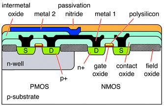
58 18.58 MOS Layout Structure L: Channel Length W: Channel Width

59 18.59 Layout crosssection CMOS Layout Structure Schematic Both nchannel (NMOS) and pchannel (PMOS) transistors are built on the same chip substrate Well: A special region created in which the semiconductor type is opposite the substrate s type Example: nwell CMOS fabrication technology to create a ntype substrate inside the already ptype substrate The nwell is used to create the PMOS transistors
60 18.60 Layers Start from the bottom up Build the n and ptype material areas on the silicon Lay the insulator layer (oxide) over the silicon Place the polysilicon (gate) on top of the oxide Connect wires to the source, gate, and drain use layers of metal above the gate 2 Layers of Metal Wires Transistor 1 Transistor 2 Side View Transistor 1 Transistor 2 Top View

61 Photolithography An IC consists of several layers of material that are manufactured in successive steps Lithography is used to selectively process the layers where the 2D mask geometry is copied on the surface Once the desired shape is patterned with photoresist the unprotected areas are etched away Liftoff and etching are different techniques to remove and shape
62 18.62 Photolithography Expose only specific areas of the chip for layer deposition or etching A layer of photoresist material is deposited on the chip Photoresist becomes soluble when exposed to ultraviolet light Using a mask to cast a shadow, some portions of photoresist can be kept while the remainder is washed away Photoresist covering silicon surface
63 18.63 Photolithography Expose only specific areas of the chip for layer deposition or etching A layer of photoresist material is deposited on the chip Photoresist becomes soluble when exposed to ultraviolet light Using a mask to cast a shadow, some portions of photoresist can be kept while the remainder is washed away Ultraviolet Light Exposed area will become soluble and be washed away exposing the surface underneath Mask creating shadow Photoresist covering silicon surface Masked area will stay hardened and protect the surface underneath
64 18.64 Ion Implantation After washing away soluble photoresist, silicon in the shape of the mask is exposed Can be implanted with ions to make n or p type material Exposed area can now be implanted with dopants Ion source bombards the exposed silicon Photoresist covering silicon surface Surface still covered by photoresist will be protected from ion implantation
65 18.65 Resulting Material After implantation, remaining photoresist can be exposed and washed away leaving n type silicon in the appropriate areas ntype doped silicon
66 18.66 Layer Deposition For layers above the surface (oxide, gate polysilicon, and metal wires), a similar but slightly different process is used 1. Entire layer of material is deposited over entire area 2. Covered with photoresist 3. Mask is used to indicate where material is desired Ultraviolet Light Photoresist layer is placed on top Mask desired material areas Oxide layer placed over entire chip area
67 18.67 Layer Deposition For layers above the surface (oxide, gate polysilicon, and metal wires), a similar but slightly different process is used 1. Entire layer of material is deposited over entire chip 2. Covered with photoresist 3. Mask is used to indicate where material is desired 4. Wash away exposed photoresist 5. Use chemical/mechanical etching process to remove exposed oxide Etching process removes exposed oxide material but cannot penetrate photoresist material Oxide layer placed over entire chip area
68 18.68 Layer Deposition For layers above the surface (oxide, gate polysilicon, and metal wires), a similar but slightly different process is used 1. Entire layer of material is deposited over entire chip 2. Covered with photoresist 3. Mask is used to indicate where material is desired 4. Wash away exposed photoresist 5. Use chemical/mechanical etching process to remove exposed oxide 6. Remaining photoresist can be removed exposing oxide in the desired location Oxide layer for gate input
69 18.69 Layer Deposition Process is repeated for gate (polysilicon) and metal wire layers A separate mask is required for each layer to indicate where the substance should be kept and where it should be etched away

70 70 Simplified CMOS Fabrication Process 18.70


71 18.71 Fabrication Images mageservice/articleimage/2003/an/b208563c/b208563cf1.gif
Outcomes. Spiral 1 / Unit 8. DeMorgan s Theorem DEMORGAN'S THEOREM. Transistor Implementations CMOS Logic Gates
 18.1 18.2 Spiral 1 / Unit 8 Transistor Implementations MOS Logic Gates Mark Redekopp Outcomes I know the difference between combinational and sequential logic and can name examples of each. I understand
Spiral Content Mapping. Spiral 1 / Unit 8. Outcomes DEMORGAN'S THEOREM. Transistor Implementations CMOS Logic Gates
 18.1 18.2 Spiral ontent Mapping Spiral Theory ombinational esign Sequential esign System Level esign Implementation and Tools Project Spiral 1 / Unit 8 Transistor Implementations MOS Logic Gates Performance
+1 (479)
") Introduction to VLSI Design http://csce.uark.edu +1 (479) 575-6043 yrpeng@uark.edu Invention of the Transistor Vacuum tubes ruled in first half of 20th century Large, expensive, power-hungry, unreliable
Introduction to VLSI Design http://csce.uark.edu +1 (479) 575-6043 yrpeng@uark.edu Invention of the Transistor Vacuum tubes ruled in first half of 20th century Large, expensive, power-hungry, unreliable
VLSI Design. Introduction
 VLSI Design Introduction Outline Introduction Silicon, pn-junctions and transistors A Brief History Operation of MOS Transistors CMOS circuits Fabrication steps for CMOS circuits Introduction Integrated
VLSI Design. Introduction
 Tassadaq Hussain VLSI Design Introduction Outcome of this course Problem Aims Objectives Outcomes Data Collection Theoretical Model Mathematical Model Validate Development Analysis and Observation Pseudo
420 Intro to VLSI Design
 Dept of Electrical and Computer Engineering 420 Intro to VLSI Design Lecture 0: Course Introduction and Overview Valencia M. Joyner Spring 2005 Getting Started Syllabus About the Instructor Labs, Problem
EE4800 CMOS Digital IC Design & Analysis. Lecture 1 Introduction Zhuo Feng
 EE4800 CMOS Digital IC Design & Analysis Lecture 1 Introduction Zhuo Feng 1.1 Prof. Zhuo Feng Office: EERC 730 Phone: 487-3116 Email: zhuofeng@mtu.edu Class Website http://www.ece.mtu.edu/~zhuofeng/ee4800fall2010.html
ENG2410 Digital Design CMOS Technology. Fall 2017 S. Areibi School of Engineering University of Guelph
 ENG2410 Digital Design CMOS Technology Fall 2017 S. reibi School of Engineering University of Guelph The Transistor Revolution First transistor Bell Labs, 1948 Bipolar logic 1960 s Intel 4004 processor
Layers. Layers. Layers. Transistor Manufacturing COMP375 1
 VLSI COMP375 Computer Architecture Middleware other CS classes Machine Language Microcode Logic circuits Transistors Middleware Machine Language - earlier Microcode Logic circuits Transistors Middleware
Lecture 0: Introduction
 Lecture 0: Introduction Introduction Integrated circuits: many transistors on one chip. Very Large Scale Integration (VLSI): bucketloads! Complementary Metal Oxide Semiconductor Fast, cheap, low power
Layers. Layers. Layers. Transistor Manufacturing COMP375 1
 Layers VLSI COMP370 Intro to Computer Architecture t Applications Middleware other CS classes High level languages Machine Language Microcode Logic circuits Gates Transistors Silicon structures Layers
Basic Fabrication Steps
 Basic Fabrication Steps and Layout Somayyeh Koohi Department of Computer Engineering Adapted with modifications from lecture notes prepared by author Outline Fabrication steps Transistor structures Transistor
Transistor was first invented by William.B.Shockley, Walter Brattain and John Bardeen of Bell Labratories. In 1961, first IC was introduced.
 Unit 1 Basic MOS Technology Transistor was first invented by William.B.Shockley, Walter Brattain and John Bardeen of Bell Labratories. In 1961, first IC was introduced. Levels of Integration:- i) SSI:-
Topic 3. CMOS Fabrication Process
 Topic 3 CMOS Fabrication Process Peter Cheung Department of Electrical & Electronic Engineering Imperial College London URL: www.ee.ic.ac.uk/pcheung/ E-mail: p.cheung@ic.ac.uk Lecture 3-1 Layout of a Inverter
Unit 3 Digital Circuits (Logic)
") Unit 3 Digital Circuits (Logic) 1 2 A Brief History COMPUTERS AND SWITCHING TECHNOLOGY 3 Mechanical Computers Primarily gearbased Difference Engine and Analytic Engine designed and partially implemented
Unit 3 Digital Circuits (Logic) 1 2 A Brief History COMPUTERS AND SWITCHING TECHNOLOGY 3 Mechanical Computers Primarily gearbased Difference Engine and Analytic Engine designed and partially implemented
Learning Outcomes. Spiral 2-6. Current, Voltage, & Resistors DIODES
 26.1 26.2 Learning Outcomes Spiral 26 Semiconductor Material MOS Theory I underst why a diode conducts current under forward bias but does not under reverse bias I underst the three modes of operation
ECE 2300 Digital Logic & Computer Organization
 ECE 2300 Digital Logic & Computer Organization Spring 2018 CMOS Logic Lecture 4: 1 NAND Logic Gate X Y (X Y) = NAND Using De Morgan s Law: (X Y) = X +Y X X X +Y = Y Y Also a NAND We can build circuits
EMT 251 Introduction to IC Design
 EMT 251 Introduction to IC Design (Pengantar Rekabentuk Litar Terkamir) Semester II 2011/2012 Introduction to IC design and Transistor Fundamental Some Keywords! Very-large-scale-integration (VLSI) is
Layout of a Inverter. Topic 3. CMOS Fabrication Process. The CMOS Process - photolithography (2) The CMOS Process - photolithography (1) v o.
 The CMOS Process - photolithography (1) v o.") Layout of a Inverter Topic 3 CMOS Fabrication Process V DD Q p Peter Cheung Department of Electrical & Electronic Engineering Imperial College London v i v o Q n URL: www.ee.ic.ac.uk/pcheung/ E-mail: p.cheung@ic.ac.uk
Layout of a Inverter Topic 3 CMOS Fabrication Process V DD Q p Peter Cheung Department of Electrical & Electronic Engineering Imperial College London v i v o Q n URL: www.ee.ic.ac.uk/pcheung/ E-mail: p.cheung@ic.ac.uk
EE 5611 Introduction to Microelectronic Technologies Fall Thursday, September 04, 2014 Lecture 02
 EE 5611 Introduction to Microelectronic Technologies Fall 2014 Thursday, September 04, 2014 Lecture 02 1 Lecture Outline Review on semiconductor materials Review on microelectronic devices Example of microelectronic
Chapter 3 Digital Logic Structures
 Chapter 3 Digital Logic Structures Transistor: Building Block of Computers Microprocessors contain millions of transistors Intel Pentium 4 (2): 48 million IBM PowerPC 75FX (22): 38 million IBM/Apple PowerPC
ECE 334: Electronic Circuits Lecture 10: Digital CMOS Circuits
 Faculty of Engineering ECE 334: Electronic Circuits Lecture 10: Digital CMOS Circuits CMOS Technology Complementary MOS, or CMOS, needs both PMOS and NMOS FET devices for their logic gates to be realized
CMOS Technology. 1. Why CMOS 2. Qualitative MOSFET model 3. Building a MOSFET 4. CMOS logic gates. Handouts: Lecture Slides. metal ndiff.
 CMOS Technology 1. Why CMOS 2. Qualitative MOSFET model 3. Building a MOSFET 4. CMOS logic gates poly pdiff metal ndiff Handouts: Lecture Slides L03 - CMOS Technology 1 Building Bits from Atoms V in V
Student Lecture by: Giangiacomo Groppi Joel Cassell Pierre Berthelot September 28 th 2004
 Student Lecture by: Giangiacomo Groppi Joel Cassell Pierre Berthelot September 28 th 2004 Lecture outline Historical introduction Semiconductor devices overview Bipolar Junction Transistor (BJT) Field
CMOS Digital Integrated Circuits Lec 2 Fabrication of MOSFETs
 CMOS Digital Integrated Circuits Lec 2 Fabrication of MOSFETs 1 CMOS Digital Integrated Circuits 3 rd Edition Categories of Materials Materials can be categorized into three main groups regarding their
INTRODUCTION TO MOS TECHNOLOGY
 INTRODUCTION TO MOS TECHNOLOGY 1. The MOS transistor The most basic element in the design of a large scale integrated circuit is the transistor. For the processes we will discuss, the type of transistor
Chapter 3: Basics Semiconductor Devices and Processing 2006/9/27 1. Topics
 Chapter 3: Basics Semiconductor Devices and Processing 2006/9/27 1 Topics What is semiconductor Basic semiconductor devices Basics of IC processing CMOS technologies 2006/9/27 2 1 What is Semiconductor
Module-3: Metal Oxide Semiconductor (MOS) & Emitter coupled logic (ECL) families
 & Emitter coupled logic (ECL) families") 1 Module-3: Metal Oxide Semiconductor (MOS) & Emitter coupled logic (ECL) families 1. Introduction 2. Metal Oxide Semiconductor (MOS) logic 2.1. Enhancement and depletion mode 2.2. NMOS and PMOS inverter
1 Module-3: Metal Oxide Semiconductor (MOS) & Emitter coupled logic (ECL) families 1. Introduction 2. Metal Oxide Semiconductor (MOS) logic 2.1. Enhancement and depletion mode 2.2. NMOS and PMOS inverter
Logic Design (Part 1) Transistors & Gates (Chapter 3)
 Transistors & Gates (Chapter 3)") Agenda next 3 weeks: Inside a microprocessor Logic Design (Part 1) Transistors & Gates (Chapter 3) Based on slides McGrawHill Additional material 2004/2005/2006 Lewis/Martin Additional material 2008 Roth
Agenda next 3 weeks: Inside a microprocessor Logic Design (Part 1) Transistors & Gates (Chapter 3) Based on slides McGrawHill Additional material 2004/2005/2006 Lewis/Martin Additional material 2008 Roth
Lecture 0: Introduction
 Introduction to CMOS VLSI Design Lecture : Introduction David Harris Steven Levitan Harvey Mudd College University of Pittsburgh Spring 24 Fall 28 Administrivia Professor Steven Levitan TA: Bo Zhao Syllabus
Introduction. Reading: Chapter 1. Courtesy of Dr. Dansereau, Dr. Brown, Dr. Vranesic, Dr. Harris, and Dr. Choi.
 Introduction Reading: Chapter 1 Courtesy of Dr. Dansereau, Dr. Brown, Dr. Vranesic, Dr. Harris, and Dr. Choi http://csce.uark.edu +1 (479) 575-6043 yrpeng@uark.edu Why study logic design? Obvious reasons
Chapter 3 Basics Semiconductor Devices and Processing
 Chapter 3 Basics Semiconductor Devices and Processing 1 Objectives Identify at least two semiconductor materials from the periodic table of elements List n-type and p-type dopants Describe a diode and
Design cycle for MEMS
 Design cycle for MEMS Design cycle for ICs IC Process Selection nmos CMOS BiCMOS ECL for logic for I/O and driver circuit for critical high speed parts of the system The Real Estate of a Wafer MOS Transistor
ECE 5745 Complex Digital ASIC Design Topic 2: CMOS Devices
 ECE 5745 Complex Digital ASIC Design Topic 2: CMOS Devices Christopher Batten School of Electrical and Computer Engineering Cornell University http://www.csl.cornell.edu/courses/ece5950 Simple Transistor
FABRICATION OF CMOS INTEGRATED CIRCUITS. Dr. Mohammed M. Farag
 FABRICATION OF CMOS INTEGRATED CIRCUITS Dr. Mohammed M. Farag Outline Overview of CMOS Fabrication Processes The CMOS Fabrication Process Flow Design Rules Reference: Uyemura, John P. "Introduction to
Chapter 3 Digital Logic Structures
 Chapter 3 Digital Logic Structures Transistor: Building Block of Computers Microprocessors contain millions of transistors Intel Pentium 4 (2000): 48 million IBM PowerPC 750FX (2002): 38 million IBM/Apple
MICROPROCESSOR TECHNOLOGY
 MICROPROCESSOR TECHNOLOGY Assis. Prof. Hossam El-Din Moustafa Lecture 3 Ch.1 The Evolution of The Microprocessor 17-Feb-15 1 Chapter Objectives Introduce the microprocessor evolution from transistors to
Chapter 3. H/w s/w interface. hardware software Vijaykumar ECE495K Lecture Notes: Chapter 3 1
 Chapter 3 hardware software H/w s/w interface Problems Algorithms Prog. Lang & Interfaces Instruction Set Architecture Microarchitecture (Organization) Circuits Devices (Transistors) Bits 29 Vijaykumar
Digital Systems Laboratory
 2012 Fall CSE140L Digital Systems Laboratory Lecture #2 by Dr. Choon Kim CSE Department, UCSD chk034@eng.ucsd.edu Lecture #2 1 Digital Technologies CPU(Central Processing Unit) GPU(Graphics Processing
TECHNO INDIA BATANAGAR (DEPARTMENT OF ELECTRONICS & COMMUNICATION ENGINEERING) QUESTION BANK- 2018
 QUESTION BANK- 2018") TECHNO INDIA BATANAGAR (DEPARTMENT OF ELECTRONICS & COMMUNICATION ENGINEERING) QUESTION BANK- 2018 Paper Setter Detail Name Designation Mobile No. E-mail ID Raina Modak Assistant Professor 6290025725 raina.modak@tib.edu.in
TECHNO INDIA BATANAGAR (DEPARTMENT OF ELECTRONICS & COMMUNICATION ENGINEERING) QUESTION BANK- 2018 Paper Setter Detail Name Designation Mobile No. E-mail ID Raina Modak Assistant Professor 6290025725 raina.modak@tib.edu.in
Chapter 2 : Semiconductor Materials & Devices (II) Feb
 Feb") Chapter 2 : Semiconductor Materials & Devices (II) 1 Reference 1. SemiconductorManufacturing Technology: Michael Quirk and Julian Serda (2001) 3. Microelectronic Circuits (5/e): Sedra & Smith (2004) 4.
Chapter 2 : Semiconductor Materials & Devices (II) 1 Reference 1. SemiconductorManufacturing Technology: Michael Quirk and Julian Serda (2001) 3. Microelectronic Circuits (5/e): Sedra & Smith (2004) 4.
Lecture 4 - Digital Representations III + Transistors
 Lecture 4 - Digital Representations III + Transistors Video: Seems like a natural extension from images no? We just have a new dimension (time) Each frame is just an image made up of pixels Display n frames
ECE/CoE 0132: FETs and Gates
 ECE/CoE 0132: FETs and Gates Kartik Mohanram September 6, 2017 1 Physical properties of gates Over the next 2 lectures, we will discuss some of the physical characteristics of integrated circuits. We will
Notes. (Subject Code: 7EC5)
") COMPUCOM INSTITUTE OF TECHNOLOGY & MANAGEMENT, JAIPUR (DEPARTMENT OF ELECTRONICS & COMMUNICATION) Notes VLSI DESIGN NOTES (Subject Code: 7EC5) Prepared By: MANVENDRA SINGH Class: B. Tech. IV Year, VII
COMPUCOM INSTITUTE OF TECHNOLOGY & MANAGEMENT, JAIPUR (DEPARTMENT OF ELECTRONICS & COMMUNICATION) Notes VLSI DESIGN NOTES (Subject Code: 7EC5) Prepared By: MANVENDRA SINGH Class: B. Tech. IV Year, VII
Microelectronics, BSc course
 Microelectronics, BSc course MOS circuits: CMOS circuits, construction http://www.eet.bme.hu/~poppe/miel/en/14-cmos.pptx http://www.eet.bme.hu The abstraction level of our study: SYSTEM + MODULE GATE CIRCUIT
Jack Keil Wolf Lecture. ESE 570: Digital Integrated Circuits and VLSI Fundamentals. Lecture Outline. MOSFET N-Type, P-Type.
 ESE 570: Digital Integrated Circuits and VLSI Fundamentals Jack Keil Wolf Lecture Lec 3: January 24, 2019 MOS Fabrication pt. 2: Design Rules and Layout http://www.ese.upenn.edu/about-ese/events/wolf.php
2009 Spring CS211 Digital Systems & Lab 1 CHAPTER 3: TECHNOLOGY (PART 2)
") 1 CHAPTER 3: IMPLEMENTATION TECHNOLOGY (PART 2) Whatwillwelearninthischapter? we learn in this 2 How transistors operate and form simple switches CMOS logic gates IC technology FPGAs and other PLDs Basic
1 CHAPTER 3: IMPLEMENTATION TECHNOLOGY (PART 2) Whatwillwelearninthischapter? we learn in this 2 How transistors operate and form simple switches CMOS logic gates IC technology FPGAs and other PLDs Basic
ECE380 Digital Logic. Logic values as voltage levels
 ECE380 Digital Logic Implementation Technology: NMOS and PMOS Transistors, CMOS logic gates Dr. D. J. Jackson Lecture 13-1 Logic values as voltage levels V ss is the minimum voltage that can exist in the
Introduction to CMOS VLSI Design (E158) Lecture 5: Logic
 Lecture 5: Logic") Harris Introduction to CMOS VLSI Design (E158) Lecture 5: Logic David Harris Harvey Mudd College David_Harris@hmc.edu Based on EE271 developed by Mark Horowitz, Stanford University MAH E158 Lecture 5 1
Harris Introduction to CMOS VLSI Design (E158) Lecture 5: Logic David Harris Harvey Mudd College David_Harris@hmc.edu Based on EE271 developed by Mark Horowitz, Stanford University MAH E158 Lecture 5 1
VLSI DESIGN AUTOMATION COURSE NOTES THE PRINCIPLES OF VLSI DESIGN
 VLSI DESIGN AUTOMATION COURSE NOTES THE PRINCIPLES OF VLSI DESIGN Peter M. Maurer ENG 118 Department of Computer Science & Engineering University of South Florida Tampa, FL 33620 1. The Nature of licon
Lecture 2: Digital Logic Basis
 Lecture 2: Digital Logic Basis Xufeng Kou School of Information Science and Technology ShanghaiTech University 1 Outline Truth Table Basic Logic Operation and Gates Logic Circuits NOR Gates and NAND Gates
ESE 570: Digital Integrated Circuits and VLSI Fundamentals
 ESE 570: Digital Integrated Circuits and VLSI Fundamentals Lec 3: January 24, 2019 MOS Fabrication pt. 2: Design Rules and Layout Penn ESE 570 Spring 2019 Khanna Jack Keil Wolf Lecture http://www.ese.upenn.edu/about-ese/events/wolf.php
Shorthand Notation for NMOS and PMOS Transistors
 Shorthand Notation for NMOS and PMOS Transistors Terminal Voltages Mode of operation depends on V g, V d, V s V gs = V g V s V gd = V g V d V ds = V d V s = V gs - V gd Source and drain are symmetric diffusion
UNIT-III GATE LEVEL DESIGN
 UNIT-III GATE LEVEL DESIGN LOGIC GATES AND OTHER COMPLEX GATES: Invert(nmos, cmos, Bicmos) NAND Gate(nmos, cmos, Bicmos) NOR Gate(nmos, cmos, Bicmos) The module (integrated circuit) is implemented in terms
Progress due to: Feature size reduction - 0.7X/3 years (Moore s Law). Increasing chip size - 16% per year. Creativity in implementing functions.
. Increasing chip size - 16% per year. Creativity in implementing functions.") Introduction - Chapter 1 Evolution of IC Fabrication 1960 and 1990 integrated t circuits. it Progress due to: Feature size reduction - 0.7X/3 years (Moore s Law). Increasing chip size - 16% per year. Creativity
Introduction - Chapter 1 Evolution of IC Fabrication 1960 and 1990 integrated t circuits. it Progress due to: Feature size reduction - 0.7X/3 years (Moore s Law). Increasing chip size - 16% per year. Creativity
Lecture Integrated circuits era
 Lecture 1 1.1 Integrated circuits era Transistor was first invented by William.B.Shockley, Walter Brattain and John Bardeen of Bell laboratories. In 1961, first IC was introduced. Levels of Integration:-
BICMOS Technology and Fabrication
 12-1 BICMOS Technology and Fabrication 12-2 Combines Bipolar and CMOS transistors in a single integrated circuit By retaining benefits of bipolar and CMOS, BiCMOS is able to achieve VLSI circuits with
Digital Design and System Implementation. Overview of Physical Implementations
 Digital Design and System Implementation Overview of Physical Implementations CMOS devices CMOS transistor circuit functional behavior Basic logic gates Transmission gates Tri-state buffers Flip-flops
Newer process technology (since 1999) includes :
 includes :") Newer process technology (since 1999) includes : copper metalization hi-k dielectrics for gate insulators si on insulator strained silicon lo-k dielectrics for interconnects Immersion lithography for masks
Newer process technology (since 1999) includes : copper metalization hi-k dielectrics for gate insulators si on insulator strained silicon lo-k dielectrics for interconnects Immersion lithography for masks
Integrated diodes. The forward voltage drop only slightly depends on the forward current. ELEKTRONIKOS ĮTAISAI
 1 Integrated diodes pn junctions of transistor structures can be used as integrated diodes. The choice of the junction is limited by the considerations of switching speed and breakdown voltage. The forward
Introduction to VLSI ASIC Design and Technology
 Introduction to VLSI ASIC Design and Technology Paulo Moreira CERN - Geneva, Switzerland Paulo Moreira Introduction 1 Outline Introduction Is there a limit? Transistors CMOS building blocks Parasitics
VLSI Designed Low Power Based DPDT Switch
 International Journal of Electronics and Communication Engineering. ISSN 0974-2166 Volume 8, Number 1 (2015), pp. 81-86 International Research Publication House http://www.irphouse.com VLSI Designed Low
Semiconductor Physics and Devices
 Metal-Semiconductor and Semiconductor Heterojunctions The Metal-Oxide-Semiconductor Field-Effect Transistor (MOSFET) is one of two major types of transistors. The MOSFET is used in digital circuit, because
CS302 - Digital Logic Design Glossary By
 CS302 - Digital Logic Design Glossary By ABEL : Advanced Boolean Expression Language; a software compiler language for SPLD programming; a type of hardware description language (HDL) Adder : A digital
Computer Architecture (TT 2012)
") Computer Architecture (TT 212) Laws of Attraction aniel Kroening Oxford University, Computer Science epartment Version 1., 212 . Kroening: Computer Architecture (TT 212) 2 . Kroening: Computer Architecture
Computer Architecture (TT 212) Laws of Attraction aniel Kroening Oxford University, Computer Science epartment Version 1., 212 . Kroening: Computer Architecture (TT 212) 2 . Kroening: Computer Architecture
ECE 410: VLSI Design Course Lecture Notes (Uyemura textbook)
") ECE 410: VLSI Design Course Lecture Notes (Uyemura tetbook) Professor Fathi Salem Michigan State University We will be updating the notes this Semester. Lecture Notes Page 2.1 Electronics Revolution Age
ECE 410: VLSI Design Course Lecture Notes (Uyemura tetbook) Professor Fathi Salem Michigan State University We will be updating the notes this Semester. Lecture Notes Page 2.1 Electronics Revolution Age
Intro to Electricity. Introduction to Transistors. Example Circuit Diagrams. Water Analogy
 Introduction to Transistors Transistors form the basic building blocks of all computer hardware. Invented by William Shockley, John Bardeen and Walter Brattain in 1947, replacing previous vaccuumtube technology
EECS 151/251A Spring 2019 Digital Design and Integrated Circuits. Instructors: Wawrzynek. Lecture 8 EE141
 EECS 151/251A Spring 2019 Digital Design and Integrated Circuits Instructors: Wawrzynek Lecture 8 EE141 From the Bottom Up IC processing CMOS Circuits (next lecture) EE141 2 Overview of Physical Implementations
Lecture 8. MOS Transistors; Cheap Computers; Everycircuit
 Lecture 8 MOS Transistors; Cheap Computers; Everycircuit Copyright 2017 by Mark Horowitz 1 Reading The rest of Chapter 4 in the reader For more details look at A&L 5.1 Digital Signals (goes in much more
QUIZ. What do these bits represent?
 QUIZ What do these bits represent? 1001 0110 1 QUIZ What do these bits represent? Unsigned integer: 1101 1110 Signed integer (2 s complement): Fraction: IBM 437 character: Latin-1 character: Huffman-compressed
Digital Integrated CircuitDesign
 Digital Integrated CircuitDesign Lecture 11 BiCMOS PMOS rray Q1 NMOS rray Y NMOS rray Q2 dib brishamifar EE Department IUST Contents Introduction BiCMOS Devices BiCMOS Inverters BiCMOS Gates BiCMOS Drivers
Power Bipolar Junction Transistors (BJTs)
") ECE442 Power Semiconductor Devices and Integrated Circuits Power Bipolar Junction Transistors (BJTs) Zheng Yang (ERF 3017, email: yangzhen@uic.edu) Power Bipolar Junction Transistor (BJT) Background The
ECE442 Power Semiconductor Devices and Integrated Circuits Power Bipolar Junction Transistors (BJTs) Zheng Yang (ERF 3017, email: yangzhen@uic.edu) Power Bipolar Junction Transistor (BJT) Background The
EE 42/100 Lecture 23: CMOS Transistors and Logic Gates. Rev A 4/15/2012 (10:39 AM) Prof. Ali M. Niknejad
 Prof. Ali M. Niknejad") A. M. Niknejad University of California, Berkeley EE 100 / 42 Lecture 23 p. 1/16 EE 42/100 Lecture 23: CMOS Transistors and Logic Gates ELECTRONICS Rev A 4/15/2012 (10:39 AM) Prof. Ali M. Niknejad University
A. M. Niknejad University of California, Berkeley EE 100 / 42 Lecture 23 p. 1/16 EE 42/100 Lecture 23: CMOS Transistors and Logic Gates ELECTRONICS Rev A 4/15/2012 (10:39 AM) Prof. Ali M. Niknejad University
Chapter 1, Introduction
 Introduction to Semiconductor Manufacturing Technology Chapter 1, Introduction hxiao89@hotmail.com 1 Objective After taking this course, you will able to Use common semiconductor terminology Describe a
EC0306 INTRODUCTION TO VLSI DESIGN
 EC0306 INTRODUCTION TO VLSI DESIGN UNIT I INTRODUCTION TO MOS CIRCUITS Why VLSI? Integration improves the design: o lower parasitics = higher speed; o lower power; o physically smaller. Integration reduces
2.8 - CMOS TECHNOLOGY
 CMOS Technology (6/7/00) Page 1 2.8 - CMOS TECHNOLOGY INTRODUCTION Objective The objective of this presentation is: 1.) Illustrate the fabrication sequence for a typical MOS transistor 2.) Show the physical
UNIT III VLSI CIRCUIT DESIGN PROCESSES. In this chapter we will be studying how to get the schematic into stick diagrams or layouts.
 UNIT III VLSI CIRCUIT DESIGN PROCESSES In this chapter we will be studying how to get the schematic into stick diagrams or layouts. MOS circuits are formed on four basic layers: N-diffusion P-diffusion
Mathematics and Science in Schools in Sub-Saharan Africa
 Mathematics and Science in Schools in Sub-Saharan Africa SEMICONDUCTORS What is a Semiconductor? What is a Semiconductor? Microprocessors LED Transistors Capacitors Range of Conduciveness The semiconductors
Semiconductor Devices
 Semiconductor Devices - 2014 Lecture Course Part of SS Module PY4P03 Dr. P. Stamenov School of Physics and CRANN, Trinity College, Dublin 2, Ireland Hilary Term, TCD 3 th of Feb 14 MOSFET Unmodified Channel
Reading. Lecture 17: MOS transistors digital. Context. Digital techniques:
 Reading Lecture 17: MOS transistors digital Today we are going to look at the analog characteristics of simple digital devices, 5. 5.4 And following the midterm, we will cover PN diodes again in forward
Learning Outcomes. Spiral 2 8. Digital Design Overview LAYOUT
 2-8.1 2-8.2 Spiral 2 8 Cell Mark Redekopp earning Outcomes I understand how a digital circuit is composed of layers of materials forming transistors and wires I understand how each layer is expressed as
EECS130 Integrated Circuit Devices
 EECS130 Integrated Circuit Devices Professor Ali Javey 11/6/2007 MOSFETs Lecture 6 BJTs- Lecture 1 Reading Assignment: Chapter 10 More Scalable Device Structures Vertical Scaling is important. For example,
UNIT-VI FIELD EFFECT TRANSISTOR. 1. Explain about the Field Effect Transistor and also mention types of FET s.
 UNIT-I FIELD EFFECT TRANSISTOR 1. Explain about the Field Effect Transistor and also mention types of FET s. The Field Effect Transistor, or simply FET however, uses the voltage that is applied to their
CMOS VLSI IC Design. A decent understanding of all tasks required to design and fabricate a chip takes years of experience
 CMOS VLSI IC Design A decent understanding of all tasks required to design and fabricate a chip takes years of experience 1 Commonly used keywords INTEGRATED CIRCUIT (IC) many transistors on one chip VERY
Integrated Circuit Technology (Course Code: EE662) Lecture 1: Introduction
 Lecture 1: Introduction") Indian Institute of Technology Jodhpur, Year 2015 2016 Integrated Circuit Technology (Course Code: EE662) Lecture 1: Introduction Course Instructor: Shree Prakash Tiwari, Ph.D. Email: sptiwari@iitj.ac.in
Indian Institute of Technology Jodhpur, Year 2015 2016 Integrated Circuit Technology (Course Code: EE662) Lecture 1: Introduction Course Instructor: Shree Prakash Tiwari, Ph.D. Email: sptiwari@iitj.ac.in
Kenneth R. Laker, University of Pennsylvania, updated 20Jan15
 http://www.seas.upenn.edu/~ese570/ 1 TOPICS The Course Industry Trends Digital CMOS Basics Some VLSI Fundamentals Illustrative Design Example 2 1. Apply principles of hierarchical digital CMOS VLSI, from
Gates and and Circuits
 Chapter 4 Gates and Circuits Chapter Goals Identify the basic gates and describe the behavior of each Describe how gates are implemented using transistors Combine basic gates into circuits Describe the
Topic 6. CMOS Static & Dynamic Logic Gates. Static CMOS Circuit. NMOS Transistors in Series/Parallel Connection
 NMOS Transistors in Series/Parallel Connection Topic 6 CMOS Static & Dynamic Logic Gates Peter Cheung Department of Electrical & Electronic Engineering Imperial College London Transistors can be thought
In this lecture we will begin a new topic namely the Metal-Oxide-Semiconductor Field Effect Transistor.
 Solid State Devices Dr. S. Karmalkar Department of Electronics and Communication Engineering Indian Institute of Technology, Madras Lecture - 38 MOS Field Effect Transistor In this lecture we will begin
Power-Area trade-off for Different CMOS Design Technologies
 Power-Area trade-off for Different CMOS Design Technologies Priyadarshini.V Department of ECE Sri Vishnu Engineering College for Women, Bhimavaram dpriya69@gmail.com Prof.G.R.L.V.N.Srinivasa Raju Head
! Review: MOS IV Curves and Switch Model. ! MOS Device Layout. ! Inverter Layout. ! Gate Layout and Stick Diagrams. ! Design Rules. !
 ESE 570: Digital Integrated Circuits and VLSI Fundamentals Lec 3: January 21, 2017 MOS Fabrication pt. 2: Design Rules and Layout Lecture Outline! Review: MOS IV Curves and Switch Model! MOS Device Layout!
Review: CMOS Logic Gates
 Review: CMOS Logic Gates INV Schematic NOR Schematic NAND Schematic + Vsg - pmos x x Vin Vout = Vin y + Vgs - nmos CMOS inverts functions CMOS Combinational Logic x g(x,y) = x + y use DeMorgan relations
! Review: MOS IV Curves and Switch Model. ! MOS Device Layout. ! Inverter Layout. ! Gate Layout and Stick Diagrams. ! Design Rules. !
 ESE 570: Digital Integrated Circuits and VLSI Fundamentals Lec 3: January 21, 2016 MOS Fabrication pt. 2: Design Rules and Layout Lecture Outline! Review: MOS IV Curves and Switch Model! MOS Device Layout!
ESE 570: Digital Integrated Circuits and VLSI Fundamentals
 ESE 570: Digital Integrated Circuits and VLSI Fundamentals Lec 3: January 21, 2016 MOS Fabrication pt. 2: Design Rules and Layout Penn ESE 570 Spring 2016 Khanna Adapted from GATech ESE3060 Slides Lecture
PAPER SOLUTION_DECEMBER_2014_VLSI_DESIGN_ETRX_SEM_VII Prepared by Girish Gidaye
 Q1a) The MOS System under External Bias Depending on the polarity and the magnitude of V G, three different operating regions can be observed for the MOS system: 1) Accumulation 2) Depletion 3) Inversion
BiCMOS Circuit Design
 BiCMOS Circuit Design 1. Introduction to BiCMOS 2. Process, Device, and Modeling 3. BiCMOS Digital Circuit Design 4. BiCMOS Analog Circuit Design 5. BiCMOS Subsystems and Practical Considerations Tai-Haur
ECE520 VLSI Design. Lecture 2: Basic MOS Physics. Payman Zarkesh-Ha
 ECE520 VLSI Design Lecture 2: Basic MOS Physics Payman Zarkesh-Ha Office: ECE Bldg. 230B Office hours: Wednesday 2:00-3:00PM or by appointment E-mail: pzarkesh@unm.edu Slide: 1 Review of Last Lecture Semiconductor
Power Spring /7/05 L11 Power 1
 Power 6.884 Spring 2005 3/7/05 L11 Power 1 Lab 2 Results Pareto-Optimal Points 6.884 Spring 2005 3/7/05 L11 Power 2 Standard Projects Two basic design projects Processor variants (based on lab1&2 testrigs)
Unit-1. MOS Transistor Theory
 VLSI DESIGN -EEE Unit-1 MOS Transistor Theory VLSI DESIGN UNIT I Contents: 1.1 Historical Perspective 1.2 What is VLSI? - Introduction 1.3 VLSI Design Flow 1.4 Design Hierarchy 1.5 Basic MOS Transistor
Gates and Circuits 1
 1 Gates and Circuits Chapter Goals Identify the basic gates and describe the behavior of each Describe how gates are implemented using transistors Combine basic gates into circuits Describe the behavior