Dynamic Logic. Domino logic P-E logic NORA logic 2-phase logic Multiple O/P domino logic Cascode logic 11/28/2012 1
|
|
|
- Rosalind Lamb
- 5 years ago
- Views:
Transcription
1 Dynamic Logic Dynamic Circuits will be introduced and their performance in terms of power, area, delay, energy and AT 2 will be reviewed. We will review the following logic families: Domino logic P-E logic NORA logic 2-phase logic Multiple O/P domino logic Cascode logic 11/28/2012 1
2 A brief introduction to Dynamic logic Dynamic logic Steady-State Behavior of Dynamic Logic Performance of Dynamic Logic Noise Considerations in Dynamic Design 11/28/2012 2

3 Dynamic Latch: Charge Leakage Stored charge leaks away due to reverse-bias current. Stored value is good for about 1 ms. Value must be rewritten to be valid. If not loaded every cycle, otherwise it must be ensured that the latch is loaded often enough to keep data valid. D X Cd+Cg X 11/28/2012 3

4 Dynamic Latch-Operation Uses complementary transmission gate to ensure that storage node is always strongly driven. Latch is transparent when transmission gate is closed. Storage capacitance comes primarily from transmission gate diffusion capacitance and inverter gate capacitance. = 0: transmission gate is off, inverter output is determined by storage node. = 1: transmission gate is on, inverter output follows D input. Setup and hold times determined by transmission gate must ensure that value stored on transmission gate is solid. 11/28/2012 4
5 Dynamic Combinational Logic Precharge/ Evaluate Networks V DD V DD M p Out M p In 1 In 2 In 3 PDN C L In 1 In 2 In 3 PUN Out M e M e C L n network p network 11/28/2012 5
6 Example of Dynamic Circuit OUTPUT A B CLK C CLK OUTPUT Precharge Evaluation Precharge 11/28/2012 6
7 General Concept Precharge and Evaluation Mp precharge transistor OUTPUT A B CLK ф C Me Evaluation transistor CLK OUTPUT Precharge Evaluation Precharge Example of nmos block For OUTPUT= (A.B + C) 11/28/2012 7
8 Charge and discharge Clock, ф A B C Output 11/28/2012 8
9 Overcoming the charge leakage and the charge sharing Mp OUTPUT A B CLK ф Me C 11/28/2012 9
10 Example continue V DD M p Out N + 1 Transistors Ratioless No Static Power Consumption A B C Noise Margins small (NM L ) Requires Clock M e 11/28/
11 Charge Leakage 11/28/
12 Charge Sharing 11/28/
13 Clock Feed through 11/28/
14 Cascading Dynamic Logic 11/28/
15 V o u t ( V o l t ) Transient Response 6.0 V out 4.0 EVALUATION PRECHARGE e e e e-09 t (nsec) 11/28/

16 4 Input NAND V DD Out In 1 In 2 In 3 In 4 GND 11/28/ Prentice Hall/Rabaey

17 Dynamic Flip-Flop D X x Y Q X X Y Q 11/28/
18 P-E logic Instead of using a static invert to ensure that 0 to 1 transitions occur during precharge, we can exploit the duality between n- block and p-block. The precharge output value of n- block equals 1, which is the correct value for the input of a p-block during precharge. All PMOS transistors of the Pull-Up Network (PUN) are turned off, so, an erroneous discharge at the on set of the evaluation phase is prevented. In a similar way, an n- block can follow a p-block without any problem, as the precharge value of inputs equals 0. To make the evaluation and precharge times of the p and n-block coincide, one has to clock the p-block with an inverted clock p. 11/28/

19 PE Logic V DD V DD M p Out M p In 1 In 2 In 3 PDN C L In 1 In 2 In 3 PUN Out M e M e C L n network p network 11/28/
20 Domino logic A Domino logic module consists of a n block followed by a static inverter. This ensures that all inputs to the next logic block are set to 0 after the precharge periods. Hence, the only possible transition during the evaluation period is 0 to 1 transition, so that formulated rule is obeyed. 11/28/

21 The block of Domino logic 11/28/
22 One Bit full Adder-Domino 11/28/
23 Simulation Results 11/28/
24 Multiple O/P Domino Logic The main concept behind MODL is the utilization of sub-functions available in the logic tree of domino gates, thus saving replication of circuitry. The additional ouputs are obtained by adding precharge devices and static inverters at the corresponding intermediate nodes of the logic tree. 11/28/
25 Multiple Output Domino C 1 = G 1 + P 1 C 0 C 2 = G 2 + P 2 C1 C 3 = G 3 + P 3 C2 C 4 = G 4 + P 4 C3 Expanding the above in terms of C1,C2,C3: C 1 = G 1 + P 1 C 0 C 2 = G 2 + P 2 (G 1 + P 1 C 0) C 3 = G 3 + P 3 (G 2 + P 2 (G 1 + P 1 C 0)) C 4 = G 4 + P 4 (G3 + P 3 (G 2 + P 2 (G 1 + P 1 C 0))) Expanding it fully C 1 = G 1 + P 1 C 0 C 2 = G 2 + P 2 G 1 + P 2 P 1 C o C 3 = G 3 + P 3 G 2 + P 3 P 2 G 1 +P 3 P 2 P 1 C 0 C 4 = G 4 + P 4 G 3 + P 4 P 3 G 2 +P 4 P 3 P 2 G 1 + P 4 P 3 P 2 P 1 C 0 11/28/

26 Multiple output Domino 11/28/

27 MODL 4-bit Carry Block C 1 = G 1 + P 1 C 0 C 2 = G 2 + P 2 G 1 + P 2 P 1 C o 11/28/2012 C 3 = G 3 + P 3 G 2 + P 3 P 2 G 1 +P 3 P 2 P 1 C 0 27 C 4 = G 4 + P 4 G 3 + P 4 P 3 G 2 +P 4 P 3 P 2 G 1 + P 4 P 3 P 2 P 1 C 0
28 2-Phase Logic We can use two-phase clock to control logic transition similar to PE. A single clock (phi1 or phi2) is used to precharge and evaluate the logic block. The succeeding stage is operated on the opposite clock phase. A latch is needed between two stages. 11/28/
29 Ø1 Evaluation Precharge Evaluation Precharge Ø2 Evaluation Precharge Evaluation Precharge ф1 Ф2 Ф1 Ф2 From ф2 stage ф1 ф1 n-logic ф2 ф2 n-logic To ф1 stage Ф1 Ф2 11/28/

30 2-Phase Domino logic 11/28/
31 NORA Logic Combining C 2 MOS pipeline register and P-E CMOS dynamic logic function block, we get NORA-CMOS (mean NO-Race). The method is suitable for the implementation of pipelined datapaths. 11/28/
32 The block of NORA logic CMOS INVER TER 11/28/
33 Cascode Logic Further refinement leads to a clocked version of the CVSL gate. This is really just two Domino gates operating on the true and complement inputs with a minimized logic tree. The advantage of this style of logic over domino logic is the ability to generate any logic expression, making it a complete logic family. This is achieved at the expense of the extra routing, active area, and complexity associated with dealing-rail logic. 11/28/
34 CASCOD Logic 11/28/
35 Comparison of 8-bit Adders Designed with Dynamic Logic Seven circuits using six dynamic logic functions are designed and simulated. The performance in terms of power, area, delay, energy and AT 2 are compared. 11/28/
36 Dynamic Logic Adders that are designed and compared Domino logic 8-bit Adder P-E logic 8-bit Adder NORA logic 8-bit Adder 2-Phase Logic 8-bit Adder Multiple O/P Domino Logic 8-bit Adder Cascode Logic 8-bit Adder 11/28/
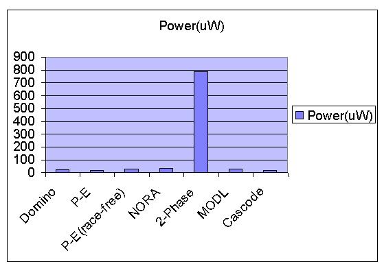
37 Power 11/28/
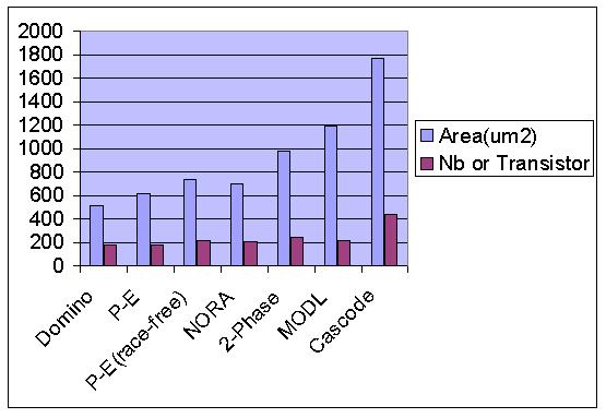
38 Area 11/28/

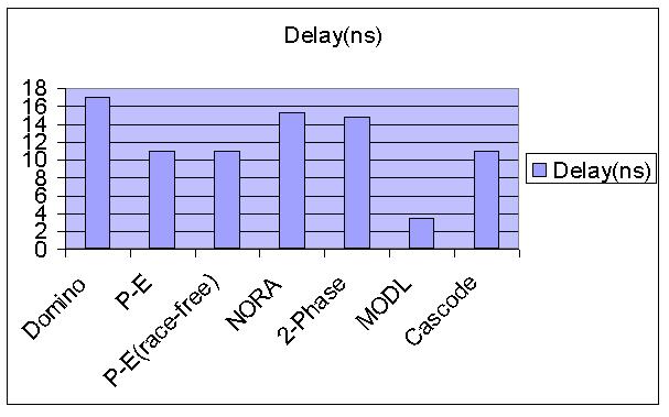
39 Delay 11/28/
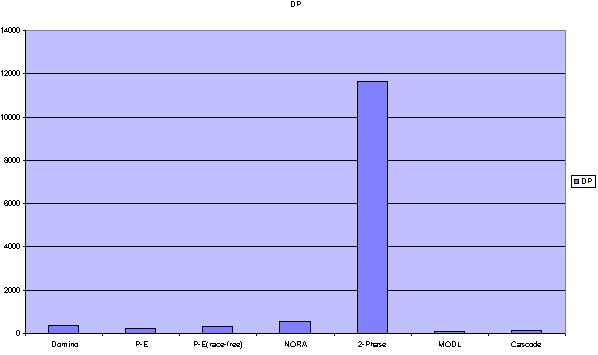
40 DP 11/28/
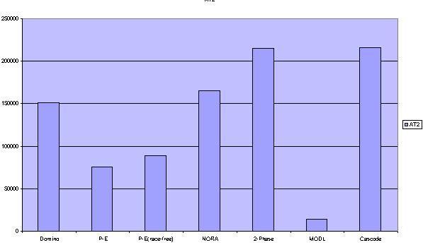
41 AT 2 11/28/
42 Conclusion Domino Logic: It has minimum area and number of transistors. The power consumption is low, and the delay is the longest. The DP and AT 2 are average. If the design goal is minimum area and speed is a secondary concern the Domino logic is the best structure for Ripple Carry Adder. 11/28/
43 Conclusion. P-E Logic: has a small area and the minimum number of transistors. The power consumption is low, and the delay is short. It has the lower DP and AT 2 for Ripple Carry Adder. If the logic has no inherent race problem, it will be the best choice for Ripple Carry Adder. 11/28/
44 Conclusion. P-E (race-free) Logic: In order to avoid the race condition of P-E Logic, the P-E (racefree) Logic is introduced. It has a small area and average of number of the transistors. The area and number of transistors is larger than P-E logic. The power consumption is average. The delay is shortest. It has lower DP and AT 2 for Ripple Carry Adder. For synthesis, it is the best choice for Ripple Carry Adder. 11/28/
45 Conclusion. NORA Logic: The power consumption is higher. The area is small, and using a few transistors except Domino logic. The delay is longer. The DP is high and AT 2 are average. 11/28/
46 Conclusion. 2-Phase Logic: The area is larger and the number of transistors is more than others except Cascode logic. The delay is longer. The power consumption, DP and AT 2 are extremely high. Try to avoid this logic structure for designing Ripple Carry Adder. 11/28/
47 Dynamic Circuits: Advantages & Disadvantages Advantages: Circuits occupy less area than the static circuits Circuits Operate at higher speed than static CMOS Circuits are Noise sensitive Drawbacks: Affected by charge sharing and charge re- distribution Always require clocks Cannot operate at low frequency Design is not straight forward 11/28/
48 FINAL WORD Thank you for being good students. I hope you have learned something in this class, that it will be useful in your future endeavor. Always go to the root of any problem that you are solving, whether engineering or social. Be a Good engineer, Never forget your Engineering ethics. Always keep your mind open to new ideas and development, and have vision as were the world is heading and try to be there before others. Do NOT forget the environment. Be a team player. Always be a dignified Engineer, respect yourself and other people s dignity. Be just to yourself and give justice to others. Always 11/28/2012 Have good intentions with your thinking, 48 actions and speaking. THANK YOU
49 Ф1 ф2 ф1 ф2 From ф2 stage Ф1 block Ф1 ф2 Ф2 block To ф1 stages Ф Ф1 ф2 11/28/
50 2-phase domino logic 11/28/
Topic 6. CMOS Static & Dynamic Logic Gates. Static CMOS Circuit. NMOS Transistors in Series/Parallel Connection
 NMOS Transistors in Series/Parallel Connection Topic 6 CMOS Static & Dynamic Logic Gates Peter Cheung Department of Electrical & Electronic Engineering Imperial College London Transistors can be thought
EEC 118 Lecture #12: Dynamic Logic
 EEC 118 Lecture #12: Dynamic Logic Rajeevan Amirtharajah University of California, Davis Jeff Parkhurst Intel Corporation Outline Today: Alternative MOS Logic Styles Dynamic MOS Logic Circuits: Rabaey
Module 4 : Propagation Delays in MOS Lecture 19 : Analyzing Delay for various Logic Circuits
 Module 4 : Propagation Delays in MOS Lecture 19 : Analyzing Delay for various Logic Circuits Objectives In this lecture you will learn the following Ratioed Logic Pass Transistor Logic Dynamic Logic Circuits
CPE/EE 427, CPE 527 VLSI Design I: Homeworks 3 & 4
 CPE/EE 427, CPE 527 VLSI Design I: Homeworks 3 & 4 1 2 3 4 5 6 7 8 9 10 Sum 30 10 25 10 30 40 10 15 15 15 200 1. (30 points) Misc, Short questions (a) (2 points) Postponing the introduction of signals
Power-Area trade-off for Different CMOS Design Technologies
 Power-Area trade-off for Different CMOS Design Technologies Priyadarshini.V Department of ECE Sri Vishnu Engineering College for Women, Bhimavaram dpriya69@gmail.com Prof.G.R.L.V.N.Srinivasa Raju Head
! Sequential Logic. ! Timing Hazards. ! Dynamic Logic. ! Add state elements (registers, latches) ! Compute. " From state elements
 ! Compute. From state elements") ESE 570: Digital Integrated Circuits and VLSI Fundamentals Lec 19: April 2, 2019 Sequential Logic, Timing Hazards and Dynamic Logic Lecture Outline! Sequential Logic! Timing Hazards! Dynamic Logic 4 Sequential
ESE 570: Digital Integrated Circuits and VLSI Fundamentals Lec 19: April 2, 2019 Sequential Logic, Timing Hazards and Dynamic Logic Lecture Outline! Sequential Logic! Timing Hazards! Dynamic Logic 4 Sequential
Chapter 6 Combinational CMOS Circuit and Logic Design. Jin-Fu Li Department of Electrical Engineering National Central University Jungli, Taiwan
 Chapter 6 Combinational CMOS Circuit and Logic Design Jin-Fu Li Department of Electrical Engineering National Central University Jungli, Taiwan Outline Advanced Reliable Systems (ARES) Lab. Jin-Fu Li,
UNIT-III GATE LEVEL DESIGN
 UNIT-III GATE LEVEL DESIGN LOGIC GATES AND OTHER COMPLEX GATES: Invert(nmos, cmos, Bicmos) NAND Gate(nmos, cmos, Bicmos) NOR Gate(nmos, cmos, Bicmos) The module (integrated circuit) is implemented in terms
! Review: Sequential MOS Logic. " SR Latch. " D-Latch. ! Timing Hazards. ! Dynamic Logic. " Domino Logic. ! Charge Sharing Setup.
 ESE 570: Digital Integrated Circuits and VLSI Fundamentals Lec 9: March 29, 206 Timing Hazards and Dynamic Logic Lecture Outline! Review: Sequential MOS Logic " SR " D-! Timing Hazards! Dynamic Logic "
EE434 ASIC & Digital Systems
 EE434 ASIC & Digital Systems Partha Pande School of EECS Washington State University pande@eecs.wsu.edu Spring 2015 Dae Hyun Kim daehyun@eecs.wsu.edu 1 Lecture 4 More on CMOS Gates Ref: Textbook chapter
Combinational Logic Gates in CMOS
 Combinational Logic Gates in CMOS References: dapted from: Digital Integrated Circuits: Design Perspective, J. Rabaey UC Principles of CMOS VLSI Design: Systems Perspective, 2nd Ed., N. H. E. Weste and
1. Short answer questions. (30) a. What impact does increasing the length of a transistor have on power and delay? Why? (6)
 a. What impact does increasing the length of a transistor have on power and delay? Why? (6)") CSE 493/593 Test 2 Fall 2011 Solution 1. Short answer questions. (30) a. What impact does increasing the length of a transistor have on power and delay? Why? (6) Decreasing of W to make the gate slower,
CSE 493/593 Test 2 Fall 2011 Solution 1. Short answer questions. (30) a. What impact does increasing the length of a transistor have on power and delay? Why? (6) Decreasing of W to make the gate slower,
Announcements. Advanced Digital Integrated Circuits. Quiz #3 today Homework #4 posted This lecture until 4pm
 EE241 - Spring 2011 dvanced Digital Integrated Circuits Lecture 20: High-Performance Logic Styles nnouncements Quiz #3 today Homework #4 posted This lecture until 4pm Reading: Chapter 8 in the owhill text
EE 330 Lecture 42. Other Logic Styles Digital Building Blocks
 EE 330 Lecture 42 Other Logic Styles Digital Building Blocks Logic Styles Static CMOS Complex Logic Gates Pass Transistor Logic (PTL) Pseudo NMOS Dynamic Logic Domino Zipper Static CMOS Widely used Attractive
! Is it feasible? ! How do we decompose the problem? ! Vdd. ! Topology. " Gate choice, logical optimization. " Fanin, fanout, Serial vs.
 ESE 570: Digital Integrated Circuits and VLSI Fundamentals Design Space Exploration Lec 18: March 28, 2017 Design Space Exploration, Synchronous MOS Logic, Timing Hazards 3 Design Problem Problem Solvable!
Design of Low Power Vlsi Circuits Using Cascode Logic Style
 Design of Low Power Vlsi Circuits Using Cascode Logic Style Revathi Loganathan 1, Deepika.P 2, Department of EST, 1 -Velalar College of Enginering & Technology, 2- Nandha Engineering College,Erode,Tamilnadu,India
Design of 32-bit ALU using Low Power Energy Efficient Full Adder Circuits
 Design of 32-bit ALU using Low Power Energy Efficient Full Adder Circuits Priyadarshini.V Department of ECE Gudlavalleru Engieering College,Gudlavalleru darshiniv708@gmail.com Ramya.P Department of ECE
IJMIE Volume 2, Issue 3 ISSN:
 IJMIE Volume 2, Issue 3 ISSN: 2249-0558 VLSI DESIGN OF LOW POWER HIGH SPEED DOMINO LOGIC Ms. Rakhi R. Agrawal* Dr. S. A. Ladhake** Abstract: Simple to implement, low cost designs in CMOS Domino logic are
Low-Power Digital CMOS Design: A Survey
 Low-Power Digital CMOS Design: A Survey Krister Landernäs June 4, 2005 Department of Computer Science and Electronics, Mälardalen University Abstract The aim of this document is to provide the reader with
EE 330 Lecture 43. Digital Circuits. Other Logic Styles Dynamic Logic Circuits
 EE 330 Lecture 43 Digital Circuits Other Logic Styles Dynamic Logic Circuits Review from Last Time Elmore Delay Calculations W M 5 V OUT x 20C RE V IN 0 L R L 1 L R R 6 W 1 C C 3 D R t 1 R R t 2 R R t
EE 330 Lecture 43. Digital Circuits. Other Logic Styles Dynamic Logic Circuits
 EE 330 Lecture 43 Digital Circuits Other Logic Styles Dynamic Logic Circuits Review from Last Time Elmore Delay Calculations W M 5 V OUT x 20C RE V IN 0 L R L 1 L R RW 6 W 1 C C 3 D R t 1 R R t 2 R R t
EE E6930 Advanced Digital Integrated Circuits. Spring, 2002 Lecture 7. Clocked and self-resetting logic I
 EE E6930 Advanced Digital Integrated Circuits Spring, 2002 Lecture 7. Clocked and self-resetting logic I References CBF, Chapter 8 DP, Section 4.3.3.1-4.3.3.4 Bernstein, High-speed CMOS design styles,
Leakage Current Analysis
 Current Analysis Hao Chen, Latriese Jackson, and Benjamin Choo ECE632 Fall 27 University of Virginia , , @virginia.edu Abstract Several common leakage current reduction methods such
Design of Robust and power Efficient 8-Bit Ripple Carry Adder using Different Logic Styles
 Design of Robust and power Efficient 8-Bit Ripple Carry Adder using Different Logic Styles Mangayarkkarasi M 1, Joseph Gladwin S 2 1 Assistant Professor, 2 Associate Professor 12 Department of ECE 1 Sri
A Low-Power High-speed Pipelined Accumulator Design Using CMOS Logic for DSP Applications
 International Journal of Research Studies in Computer Science and Engineering (IJRSCSE) Volume. 1, Issue 5, September 2014, PP 30-42 ISSN 2349-4840 (Print) & ISSN 2349-4859 (Online) www.arcjournals.org
Designing of Low-Power VLSI Circuits using Non-Clocked Logic Style
 International Journal of Advancements in Research & Technology, Volume 1, Issue3, August-2012 1 Designing of Low-Power VLSI Circuits using Non-Clocked Logic Style Vishal Sharma #, Jitendra Kaushal Srivastava
UNIT-II LOW POWER VLSI DESIGN APPROACHES
 UNIT-II LOW POWER VLSI DESIGN APPROACHES Low power Design through Voltage Scaling: The switching power dissipation in CMOS digital integrated circuits is a strong function of the power supply voltage.
ECE 334: Electronic Circuits Lecture 10: Digital CMOS Circuits
 Faculty of Engineering ECE 334: Electronic Circuits Lecture 10: Digital CMOS Circuits CMOS Technology Complementary MOS, or CMOS, needs both PMOS and NMOS FET devices for their logic gates to be realized
Electronics Basic CMOS digital circuits
 Electronics Basic CMOS digital circuits Prof. Márta Rencz, Gábor Takács, Dr. György Bognár, Dr. Péter G. Szabó BME DED October 21, 2014 1 / 30 Introduction The topics covered today: The inverter: the simplest
ECE380 Digital Logic. Logic values as voltage levels
 ECE380 Digital Logic Implementation Technology: NMOS and PMOS Transistors, CMOS logic gates Dr. D. J. Jackson Lecture 13-1 Logic values as voltage levels V ss is the minimum voltage that can exist in the
COMPREHENSIVE ANALYSIS OF ENHANCED CARRY-LOOK AHEAD ADDER USING DIFFERENT LOGIC STYLES
 COMPREHENSIVE ANALYSIS OF ENHANCED CARRY-LOOK AHEAD ADDER USING DIFFERENT LOGIC STYLES PSowmya #1, Pia Sarah George #2, Samyuktha T #3, Nikita Grover #4, Mrs Manurathi *1 # BTech,Electronics and Communication,Karunya
EEC 118 Lecture #11: CMOS Design Guidelines Alternative Static Logic Families
 EEC 118 Lecture #11: CMOS Design Guidelines Alternative Static Logic Families Rajeevan Amirtharajah University of California, Davis Jeff Parkhurst Intel Corporation Announcements Homework 5 this week Lab
EE 330 Lecture 44. Digital Circuits. Other Logic Styles Dynamic Logic Circuits
 EE 330 Lecture 44 Digital Circuits Other Logic Styles Dynamic Logic Circuits Course Evaluation Reminder - ll Electronic http://bit.ly/isustudentevals Review from Last Time Power Dissipation in Logic Circuits
Performance Analysis of High Speed Low Power Carry Look-Ahead Adder Using Different Logic Styles
 International Journal of Soft Computing and Engineering (IJSCE) ISSN: 2231-237, Volume-2, Issue-6, Jan- 213 Performance Analysis of High Speed Low Power Carry Look-Ahead Adder Using Different Logic Styles
Noise Tolerance Dynamic CMOS Logic Design with Current Mirror Circuit
 International Journal of Electrical Engineering. ISSN 0974-2158 Volume 7, Number 1 (2014), pp. 77-81 International Research Publication House http://www.irphouse.com Noise Tolerance Dynamic CMOS Logic
A HIGH SPEED DYNAMIC RIPPLE CARRY ADDER
 A HIGH SPEED DYNAMIC RIPPLE CARRY ADDER Y. Anil Kumar 1, M. Satyanarayana 2 1 Student, Department of ECE, MVGR College of Engineering, India. 2 Associate Professor, Department of ECE, MVGR College of Engineering,
Chapter 3 DESIGN OF ADIABATIC CIRCUIT. 3.1 Introduction
 Chapter 3 DESIGN OF ADIABATIC CIRCUIT 3.1 Introduction The details of the initial experimental work carried out to understand the energy recovery adiabatic principle are presented in this section. This
Novel Low-Overhead Operand Isolation Techniques for Low-Power Datapath Synthesis
 Novel Low-Overhead Operand Isolation Techniques for Low-Power Datapath Synthesis N. Banerjee, A. Raychowdhury, S. Bhunia, H. Mahmoodi, and K. Roy School of Electrical and Computer Engineering, Purdue University,
EE 42/100 Lecture 24: Latches and Flip Flops. Rev A 4/14/2010 (8:30 PM) Prof. Ali M. Niknejad
 Prof. Ali M. Niknejad") A. M. Niknejad University of California, Berkeley EE 100 / 42 Lecture 24 p. 1/15 EE 42/100 Lecture 24: Latches and Flip Flops ELECTRONICS Rev A 4/14/2010 (8:30 PM) Prof. Ali M. Niknejad University of California,
A. M. Niknejad University of California, Berkeley EE 100 / 42 Lecture 24 p. 1/15 EE 42/100 Lecture 24: Latches and Flip Flops ELECTRONICS Rev A 4/14/2010 (8:30 PM) Prof. Ali M. Niknejad University of California,
Domino Static Gates Final Design Report
 Domino Static Gates Final Design Report Krishna Santhanam bstract Static circuit gates are the standard circuit devices used to build the major parts of digital circuits. Dynamic gates, such as domino
Electronic Circuits EE359A
 Electronic Circuits EE359A Bruce McNair B206 bmcnair@stevens.edu 201-216-5549 1 Memory and Advanced Digital Circuits - 2 Chapter 11 2 Figure 11.1 (a) Basic latch. (b) The latch with the feedback loop opened.
CMOS Digital Integrated Circuits Analysis and Design
 CMOS Digital Integrated Circuits Analysis and Design Chapter 8 Sequential MOS Logic Circuits 1 Introduction Combinational logic circuit Lack the capability of storing any previous events Non-regenerative
Domino CMOS Implementation of Power Optimized and High Performance CLA adder
 Domino CMOS Implementation of Power Optimized and High Performance CLA adder Kistipati Karthik Reddy 1, Jeeru Dinesh Reddy 2 1 PG Student, BMS College of Engineering, Bull temple Road, Bengaluru, India
International Journal of Advanced Research in Biology Engineering Science and Technology (IJARBEST)
") Abstract NEW HIGH PERFORMANCE 4 BIT PARALLEL ADDER USING DOMINO LOGIC Department Of Electronics and Communication Engineering UG Scholar, SNS College of Engineering Bhuvaneswari.N [1], Hemalatha.V [2],
Abstract NEW HIGH PERFORMANCE 4 BIT PARALLEL ADDER USING DOMINO LOGIC Department Of Electronics and Communication Engineering UG Scholar, SNS College of Engineering Bhuvaneswari.N [1], Hemalatha.V [2],
Low Power, Area Efficient FinFET Circuit Design
 Low Power, Area Efficient FinFET Circuit Design Michael C. Wang, Princeton University Abstract FinFET, which is a double-gate field effect transistor (DGFET), is more versatile than traditional single-gate
ISSN: [Kumar* et al., 6(5): May, 2017] Impact Factor: 4.116
![ISSN: [Kumar* et al., 6(5): May, 2017] Impact Factor: 4.116](/thumbs/96/126774931.jpg "ISSN: [Kumar* et al., 6(5): May, 2017] Impact Factor: 4.116") IJESRT INTERNATIONAL JOURNAL OF ENGINEERING SCIENCES & RESEARCH TECHNOLOGY IMPROVEMENT IN NOISE AND DELAY IN DOMINO CMOS LOGIC CIRCUIT Ankit Kumar*, Dr. A.K. Gautam * Student, M.Tech. (ECE), S.D. College
IJESRT INTERNATIONAL JOURNAL OF ENGINEERING SCIENCES & RESEARCH TECHNOLOGY IMPROVEMENT IN NOISE AND DELAY IN DOMINO CMOS LOGIC CIRCUIT Ankit Kumar*, Dr. A.K. Gautam * Student, M.Tech. (ECE), S.D. College
A Low Power Array Multiplier Design using Modified Gate Diffusion Input (GDI)
") A Low Power Array Multiplier Design using Modified Gate Diffusion Input (GDI) Mahendra Kumar Lariya 1, D. K. Mishra 2 1 M.Tech, Electronics and instrumentation Engineering, Shri G. S. Institute of Technology
A Low Power Array Multiplier Design using Modified Gate Diffusion Input (GDI) Mahendra Kumar Lariya 1, D. K. Mishra 2 1 M.Tech, Electronics and instrumentation Engineering, Shri G. S. Institute of Technology
Design of High Performance Arithmetic and Logic Circuits in DSM Technology
 Design of High Performance Arithmetic and Logic Circuits in DSM Technology Salendra.Govindarajulu 1, Dr.T.Jayachandra Prasad 2, N.Ramanjaneyulu 3 1 Associate Professor, ECE, RGMCET, Nandyal, JNTU, A.P.Email:
Digital Microelectronic Circuits ( ) Pass Transistor Logic. Lecture 9: Presented by: Adam Teman
 Pass Transistor Logic. Lecture 9: Presented by: Adam Teman") Digital Microelectronic Circuits (361-1-3021 ) Presented by: Adam Teman Lecture 9: Pass Transistor Logic 1 Motivation In the previous lectures, we learned about Standard CMOS Digital Logic design. CMOS
Digital Microelectronic Circuits (361-1-3021 ) Presented by: Adam Teman Lecture 9: Pass Transistor Logic 1 Motivation In the previous lectures, we learned about Standard CMOS Digital Logic design. CMOS
EE241 - Spring 2002 Advanced Digital Integrated Circuits
 EE241 - Spring 2002 dvanced Digital Integrated Circuits Lecture 7 MOS Logic Styles nnouncements Homework #1 due 2/19 1 Reading Chapter 7 in the text by K. ernstein ackground material from Rabaey References»
CHAPTER 5 DESIGN AND ANALYSIS OF COMPLEMENTARY PASS- TRANSISTOR WITH ASYNCHRONOUS ADIABATIC LOGIC CIRCUITS
 70 CHAPTER 5 DESIGN AND ANALYSIS OF COMPLEMENTARY PASS- TRANSISTOR WITH ASYNCHRONOUS ADIABATIC LOGIC CIRCUITS A novel approach of full adder and multipliers circuits using Complementary Pass Transistor
Performance Comparison of High-Speed Adders Using 180nm Technology
 Steena Maria Thomas et al. 2016, Volume 4 Issue 2 ISSN (Online): 2348-4098 ISSN (Print): 2395-4752 International Journal of Science, Engineering and Technology An Open Access Journal Performance Comparison
CHAPTER 3 PERFORMANCE OF A TWO INPUT NAND GATE USING SUBTHRESHOLD LEAKAGE CONTROL TECHNIQUES
 CHAPTER 3 PERFORMANCE OF A TWO INPUT NAND GATE USING SUBTHRESHOLD LEAKAGE CONTROL TECHNIQUES 41 In this chapter, performance characteristics of a two input NAND gate using existing subthreshold leakage
ECE 471/571 The CMOS Inverter Lecture-6. Gurjeet Singh
 ECE 471/571 The CMOS Inverter Lecture-6 Gurjeet Singh NMOS-to-PMOS ratio,pmos are made β times larger than NMOS Sizing Inverters for Performance Conclusions: Intrinsic delay tp0 is independent of sizing
Lecture 16. Complementary metal oxide semiconductor (CMOS) CMOS 1-1
 CMOS 1-1") Lecture 16 Complementary metal oxide semiconductor (CMOS) CMOS 1-1 Outline Complementary metal oxide semiconductor (CMOS) Inverting circuit Properties Operating points Propagation delay Power dissipation
Lecture 16 Complementary metal oxide semiconductor (CMOS) CMOS 1-1 Outline Complementary metal oxide semiconductor (CMOS) Inverting circuit Properties Operating points Propagation delay Power dissipation
Contents 1 Introduction 2 MOS Fabrication Technology
 Contents 1 Introduction... 1 1.1 Introduction... 1 1.2 Historical Background [1]... 2 1.3 Why Low Power? [2]... 7 1.4 Sources of Power Dissipations [3]... 9 1.4.1 Dynamic Power... 10 1.4.2 Static Power...
Propagation Delay, Circuit Timing & Adder Design. ECE 152A Winter 2012
 Propagation Delay, Circuit Timing & Adder Design ECE 152A Winter 2012 Reading Assignment Brown and Vranesic 2 Introduction to Logic Circuits 2.9 Introduction to CAD Tools 2.9.1 Design Entry 2.9.2 Synthesis
Propagation Delay, Circuit Timing & Adder Design
 Propagation Delay, Circuit Timing & Adder Design ECE 152A Winter 2012 Reading Assignment Brown and Vranesic 2 Introduction to Logic Circuits 2.9 Introduction to CAD Tools 2.9.1 Design Entry 2.9.2 Synthesis
Introduction to Electronic Devices
 Introduction to Electronic Devices (Course Number 300331) Fall 2006 Dr. Dietmar Knipp Assistant Professor of Electrical Engineering Information: http://www.faculty.iubremen.de/dknipp/ Source: Apple Ref.:
Investigation on Performance of high speed CMOS Full adder Circuits
 ISSN (O): 2349-7084 International Journal of Computer Engineering In Research Trends Available online at: www.ijcert.org Investigation on Performance of high speed CMOS Full adder Circuits 1 KATTUPALLI
MOS Logic and Gate Circuits. Wired OR
 MOS Logic and Gate Circuits A A A B A AB Y Wired OR Contents Introduction NMOS Logic Resistive Load Saturated Enhancement Load Linear Enhancement Load Depletion Load Some Gates Transient in NMOS Circuit
Jan Rabaey, «Low Powere Design Essentials," Springer tml
 Jan Rabaey, «e Design Essentials," Springer 2009 http://web.me.com/janrabaey/lowpoweressentials/home.h tml Dimitrios Soudris, Christian Piguet, and Costas Goutis, Designing CMOS Circuits for Low POwer,
EC 1354-Principles of VLSI Design
 EC 1354-Principles of VLSI Design UNIT I MOS TRANSISTOR THEORY AND PROCESS TECHNOLOGY PART-A 1. What are the four generations of integrated circuits? 2. Give the advantages of IC. 3. Give the variety of
DIGITAL INTEGRATED CIRCUITS A DESIGN PERSPECTIVE 2 N D E D I T I O N
 DIGITAL INTEGRATED CIRCUITS A DESIGN PERSPECTIVE 2 N D E D I T I O N Jan M. Rabaey, Anantha Chandrakasan, and Borivoje Nikolic CONTENTS PART I: THE FABRICS Chapter 1: Introduction (32 pages) 1.1 A Historical
The Effect of Threshold Voltages on the Soft Error Rate. - V Degalahal, N Rajaram, N Vijaykrishnan, Y Xie, MJ Irwin
 The Effect of Threshold Voltages on the Soft Error Rate - V Degalahal, N Rajaram, N Vijaykrishnan, Y Xie, MJ Irwin Outline Introduction Soft Errors High Threshold ( V t ) Charge Creation Logic Attenuation
Reduced Swing Domino Techniques for Low Power and High Performance Arithmetic Circuits
 Reduced Swing Domino Techniques for Low Power and High Performance Arithmetic Circuits by Shahrzad Naraghi A thesis presented to the University of Waterloo in fulfillment of the thesis requirement for
International Journal of Advanced Research in Computer Science and Software Engineering
 Volume 3, Issue 8, August 2013 ISSN: 2277 128X International Journal of Advanced Research in Computer Science and Software Engineering Research Paper Available online at: www.ijarcsse.com A Novel Implementation
DESIGN OF LOW POWER MULTIPLIER USING COMPOUND CONSTANT DELAY LOGIC STYLE
 DESIGN OF LOW POWER MULTIPLIER USING COMPOUND CONSTANT DELAY LOGIC STYLE 1 S. DARWIN, 2 A. BENO, 3 L. VIJAYA LAKSHMI 1 & 2 Assistant Professor Electronics & Communication Engineering Department, Dr. Sivanthi
Performance Evaluation of Adders using LP-HS Logic in CMOS Technologies
 Performance Evaluation of Adders using LP-HS Logic in CMOS Technologies Linet K 1, Umarani P 1, T.Ravi 1 1 Scholar, Department of ECE, Sathyabama university E-mail- linetk2910@gmail.com ABSTRACT - This
Practice 6: CMOS Digital Logic
 Practice 6: CMOS Digital Logic Digital Electronic Circuits Semester A 2012 The MOSFET as a Switch The MOSFET as a Switch We can look at the MOSFET as a Switch, passing the data between the diffusions when
EE584 Introduction to VLSI Design Final Project Document Group 9 Ring Oscillator with Frequency selector
 EE584 Introduction to VLSI Design Final Project Document Group 9 Ring Oscillator with Frequency selector Group Members Uttam Kumar Boda Rajesh Tenukuntla Mohammad M Iftakhar Srikanth Yanamanagandla 1 Table
2-Bit Magnitude Comparator Design Using Different Logic Styles
 International Journal of Engineering Science Invention ISSN (Online): 2319 6734, ISSN (Print): 2319 6726 Volume 2 Issue 1 ǁ January. 2013 ǁ PP.13-24 2-Bit Magnitude Comparator Design Using Different Logic
Lecture 4. The CMOS Inverter. DC Transfer Curve: Load line. DC Operation: Voltage Transfer Characteristic. Noise in Digital Integrated Circuits
 Noise in Digital Integrated Circuits Lecture 4 The CMOS Inverter i(t) v(t) V DD Peter Cheung Department of Electrical & Electronic Engineering Imperial College London URL: www.ee.ic.ac.uk/pcheung/ E-mail:
EE 42/100 Lecture 23: CMOS Transistors and Logic Gates. Rev A 4/15/2012 (10:39 AM) Prof. Ali M. Niknejad
 Prof. Ali M. Niknejad") A. M. Niknejad University of California, Berkeley EE 100 / 42 Lecture 23 p. 1/16 EE 42/100 Lecture 23: CMOS Transistors and Logic Gates ELECTRONICS Rev A 4/15/2012 (10:39 AM) Prof. Ali M. Niknejad University
A. M. Niknejad University of California, Berkeley EE 100 / 42 Lecture 23 p. 1/16 EE 42/100 Lecture 23: CMOS Transistors and Logic Gates ELECTRONICS Rev A 4/15/2012 (10:39 AM) Prof. Ali M. Niknejad University
A Novel Low-Power Scan Design Technique Using Supply Gating
 A Novel Low-Power Scan Design Technique Using Supply Gating S. Bhunia, H. Mahmoodi, S. Mukhopadhyay, D. Ghosh, and K. Roy School of Electrical and Computer Engineering, Purdue University, West Lafayette,
A Survey of the Low Power Design Techniques at the Circuit Level
 A Survey of the Low Power Design Techniques at the Circuit Level Hari Krishna B Assistant Professor, Department of Electronics and Communication Engineering, Vagdevi Engineering College, Warangal, India
ECE520 VLSI Design. Lecture 11: Combinational Static Logic. Prof. Payman Zarkesh-Ha
 EE520 VLSI esign Lecture 11: ombinational Static Logic Prof. Payman Zarkesh-Ha Office: EE ldg. 230 Office hours: Wednesday 2:00-3:00PM or by appointment E-mail: pzarkesh@unm.edu Slide: 1 eview of Last
VLSI Logic Structures
 VLSI Logic Structures Ratioed Logic Pass-Transistor Logic Dynamic CMOS Domino Logic Zipper CMOS Spring 25 John. Chandy inary Multiplication + x Multiplicand Multiplier Partial products Result Spring 25
EE 42/100 Lecture 24: Latches and Flip Flops. Rev B 4/21/2010 (2:04 PM) Prof. Ali M. Niknejad
 Prof. Ali M. Niknejad") A. M. Niknejad University of California, Berkeley EE 100 / 42 Lecture 24 p. 1/21 EE 42/100 Lecture 24: Latches and Flip Flops ELECTRONICS Rev B 4/21/2010 (2:04 PM) Prof. Ali M. Niknejad University of California,
A. M. Niknejad University of California, Berkeley EE 100 / 42 Lecture 24 p. 1/21 EE 42/100 Lecture 24: Latches and Flip Flops ELECTRONICS Rev B 4/21/2010 (2:04 PM) Prof. Ali M. Niknejad University of California,
DESIGN OF CARRY LOOK AHEAD ADDER USING SUB THRESHOLD DUAL MODE LOGIC
 DESIGN OF CARRY LOOK AHEAD ADDER USING SUB THRESHOLD DUAL MODE LOGIC Ms. S.A. Ameena Nasreen Electronics and Communication Engineering, NPR College of Engineering and Technology, Dindigul, Tamilnadu, India
Lecture 9: Clocking for High Performance Processors
 Lecture 9: Clocking for High Performance Processors Computer Systems Lab Stanford University horowitz@stanford.edu Copyright 2001 Mark Horowitz EE371 Lecture 9-1 Horowitz Overview Reading Bailey Stojanovic
CHAPTER 3 NEW SLEEPY- PASS GATE
 56 CHAPTER 3 NEW SLEEPY- PASS GATE 3.1 INTRODUCTION A circuit level design technique is presented in this chapter to reduce the overall leakage power in conventional CMOS cells. The new leakage po leepy-
Integrated Circuits & Systems
 Federal University of Santa atarina enter for Technology omputer Science & Electronics Engineering Integrated ircuits & Systems INE 5442 Lecture 16 MOS ombinational ircuits - 2 guntzel@inf.ufsc.br Pass
IMPLEMENTATION OF LOW POWER AND LOW ENERGY SYNCHRONOUS SAPT LOGIC
 IMPLEMENTATION OF LOW POWER AND LOW ENERGY SYNCHRONOUS SAPT LOGIC Chitambara Rao.K 1,Nagendra.K 2 Sreenivasa Rao.Ijjada 3 1 Department of ECE, AITAM College of Engineering, Tekkali, Srikakulam,India rao_chidu@ymail.com
A Novel Approach for High Speed and Low Power 4-Bit Multiplier
 IOSR Journal of VLSI and Signal Processing (IOSR-JVSP) ISSN: 2319 4200, ISBN No. : 2319 4197 Volume 1, Issue 3 (Nov. - Dec. 2012), PP 13-26 A Novel Approach for High Speed and Low Power 4-Bit Multiplier
Sleepy Keeper Approach for Power Performance Tuning in VLSI Design
 International Journal of Electronics and Communication Engineering. ISSN 0974-2166 Volume 6, Number 1 (2013), pp. 17-28 International Research Publication House http://www.irphouse.com Sleepy Keeper Approach
BASIC PHYSICAL DESIGN AN OVERVIEW The VLSI design flow for any IC design is as follows
 Unit 3 BASIC PHYSICAL DESIGN AN OVERVIEW The VLSI design flow for any IC design is as follows 1.Specification (problem definition) 2.Schematic(gate level design) (equivalence check) 3.Layout (equivalence
Chapter 2 Combinational Circuits
 Chapter 2 Combinational Circuits SKEE2263 Digital Systems Mun im/ismahani/izam {munim@utm.my,e-izam@utm.my,ismahani@fke.utm.my} February 23, 26 Why CMOS? Most logic design today is done on CMOS circuits
ECE/CoE 0132: FETs and Gates
 ECE/CoE 0132: FETs and Gates Kartik Mohanram September 6, 2017 1 Physical properties of gates Over the next 2 lectures, we will discuss some of the physical characteristics of integrated circuits. We will
Design & Analysis of Low Power Full Adder
 1174 Design & Analysis of Low Power Full Adder Sana Fazal 1, Mohd Ahmer 2 1 Electronics & communication Engineering Integral University, Lucknow 2 Electronics & communication Engineering Integral University,
EE141-Spring 2007 Digital Integrated Circuits
 EE141-Spring 2007 Digital Integrated Circuits Lecture 22 I/O, Power Distribution dders 1 nnouncements Homework 9 has been posted Due Tu. pr. 24, 5pm Project Phase 4 (Final) Report due Mo. pr. 30, noon
Power Efficient and Noise Immune Domino Logic for Wide Fan in Gates
 Power Efficient and Noise Immune Domino Logic for Wide Fan in Gates K.Venkata laxmi¹, B.Lakshmi² PG Student [VLSI], Dept. of ECE, GVP College of Engineering, Visakhapatnam, Andhra Pradesh, India 1 Assistant
Circuits in CMOS VLSI. Darshana Sankhe
 Circuits in CMOS VLSI Darshana Sankhe Static CMOS Advantages: Static (robust) operation, low power, scalable with technology. Disadvantages: Large size: An N input gate requires 2N transistors. Large capacitance:
COMPARATIVE ANALYSIS OF 32 BIT CARRY LOOK AHEAD ADDER USING HIGH SPEED CONSTANT DELAY LOGIC
 COMPARATIVE ANALYSIS OF 32 BIT CARRY LOOK AHEAD ADDER USING HIGH SPEED CONSTANT DELAY LOGIC V.Reethika Rao (1), Dr.K.Ragini (2) PG Scholar, Dept of ECE, G. Narayanamma Institute of Technology and Science,
Department of Electrical and Computer Systems Engineering
 Department of Electrical and Computer Systems Engineering Technical Report MECSE-31-2005 Asynchronous Self Timed Processing: Improving Performance and Design Practicality D. Browne and L. Kleeman Asynchronous
Ultra Low Power VLSI Design: A Review
 International Journal of Emerging Engineering Research and Technology Volume 4, Issue 3, March 2016, PP 11-18 ISSN 2349-4395 (Print) & ISSN 2349-4409 (Online) Ultra Low Power VLSI Design: A Review G.Bharathi
Design of Multipliers Using Low Power High Speed Logic in CMOS Technologies
 Design of Multipliers Using Low Power High Speed Logic in CMOS Technologies Linet. K 1, Umarani.P 2, T. Ravi 3 M.Tech VLSI Design, Dept. of ECE, Sathyabama University, Chennai, Tamilnadu, India 1 Assistant
of Tech in & Embe by
 Analysis and Application of Improved Feedthrough Logic A Thesis Submitted in Partiall Fulfillment of the RequiremeR ents for the Awardd of the Degree of Master VLSI Design & of Tech in & Embe by hnologyy
Design of Low Power High Speed Fully Dynamic CMOS Latched Comparator
 International Journal of Engineering Research and Development e-issn: 2278-067X, p-issn: 2278-800X, www.ijerd.com Volume 10, Issue 4 (April 2014), PP.01-06 Design of Low Power High Speed Fully Dynamic
A Low Power and Area Efficient Full Adder Design Using GDI Multiplexer
 A Low Power and Area Efficient Full Adder Design Using GDI Multiplexer G.Bramhini M.Tech (VLSI), Vidya Jyothi Institute of Technology. G.Ravi Kumar, M.Tech Assistant Professor, Vidya Jyothi Institute of