Integration, Architecture, and Applications of 3D CMOS Memristor Circuits
|
|
|
- Linette Arnold
- 6 years ago
- Views:
Transcription
1 Integration, Architecture, and Applications of 3D CMOS Memristor Circuits K. T. Tim Cheng and Dimitri Strukov Univ. of California, Santa Barbara ISPD

2 3D Hybrid CMOS/NANO add-on nanodevices layer CMOS layer CMOS stack bottom nanowire level top nanowire level similar two-terminal nanodevices at each crosspoint CMOS stack + nano add-on nanowire crossbar of two-terminal devices (memristors) 2

 200 100")
 3 J. Yang Iet al. Natue Nano, (2008)")
3 Resistive Switching Memristive Devices (latching switches, a.k.a. resistive switches, a.k.a. programmable diodes, a.k.a. memristive switches) +Wide range of material systems and physical phenomena Current ( ua ) nm hp 0 + Pt 100 TiO 2 V <50 ns TiO x Pt Voltage ( V ) 3 J. Yang Iet al. Natue Nano, (2008)
 MOSFET Si wafer K. Likharev (2004, 2005); D. Strukov and K. Likharev (2006) http://www.oxfordplasma.de/ process/sibo_wtc.htm 4")
4 Area Distributed CMOL Interfaces interface via ( pin ) nanodevices (latching switches) gold nanowire levels (nanoimprint) interface pins Tip radii 2-10 nm CMOS stack (just a cartoon) MOSFET Si wafer K. Likharev (2004, 2005); D. Strukov and K. Likharev (2006) process/sibo_wtc.htm 4
5 AFOSR MURI HyNano: 3D Hybrid CMOS Nano Circuits 5


6 The HyNano Team Michael Chabinyc Materials, UCSB Tim Cheng ECE, UCSB (Director) Marivi Fernandez Serra Physics, Stony Brook Konstantin K. Likharev Physics, Stony Brook Wei Lu EECS, Michigan Susanne Stemmer Materials, UCSB Dmitri Strukov ECE, UCSB Luke Theogarajan ECE, UCSB Qiangfei Xia ECE, UM Amherst 6
7 Project Overview information processing APPLICATIONS 3D hybrid memories 3D hybrid SoC ARCHITECTURES/CIRCUITS 3D CMOS/nano circuits w. area distributed interface mixed signal CrossNets Optical lithography a Si e beam metal oxide nanoimprint reproducible, high performance, high endurance devices MATERIALS organic DEVICES solid electrolyte compact models drift diffusion and ab initio modeling 7


8 Thrust Area #1: Application/Architecture/Ckt Exploration Memory arrays for high performance computing CMOL based FPGA Neuromorphic networks for bio inspired information processing Evolvable analog circuits Tunable bias network for analog design Weighted multiply and add circuits High precision Digital to Analog converter 8
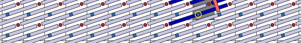
9 CMOL Interface Integrating CMOS with Crossbar Memory Array interface via ( pin ) nanodevices (latching switches) gold nanowire levels (nanoimprint) interface pins CMOS stack (just a cartoon) MOSFET Si wafer

10 Addressing Crossbar Memory Array There are two types of pins Blues and Reds Each array of pins has its own decoding scheme Double decoding scheme: An array of N 2 blue pins uniquely accessed with 2N control signals. Another 2N control signals for the corresponding N 2 red pins
11 Double Decoding Scheme Four decoders: demux memory cell array select decoder select decoder mux/demux data I/O 11
12 Crossbar Construction Top View
13 Crossbar Construction Top View
14 Crossbar Construction Side View interface via ( pin ) nanodevices (latching switches) gold nanowire levels (nanoimprint) interface pins CMOS stack (just a cartoon) MOSFET Si wafer
15 Crossbar Construction Top View
16 Crossbar Construction Bottom Level
17 Crossbar Construction Top Level
18 Crossbar Construction
19 Crossbar Construction
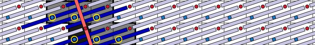
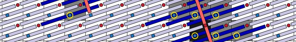
20 Crossbar Construction Connectivity Domain
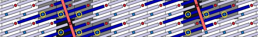
21 Crossbar Construction
22 Crossbar Construction
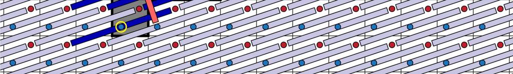
23 Unused Address Space The red pin can only interact with blue pins in its connectivity domain Address space provided by yellow cells is wasted!
24 Key Geometric Parameters Distance between nanowires is 2F NANO Size of cell is 2βF CMOS β 2 = r where r is an odd integer > 1. Crossbar is tilted by an angle α equal to ArcTan(1/r) with respect to the pins. # of reachable crosspoints per wire segment is r 2 1
25 Crossbar Construction Bottom Level


26 Adding a Second Crossbar Layer Connectivity domain in the first crossbar layer Connectivity domain in the second crossbar layer The mapping is done through pin translation wires Blue pins are common to all crossbar layers. Red pins are "redefined" for each layer using the pin translation wires.


27 First layer of red pins.

28 First layer of red and blue pins.
29 Layer of (bluish) wires connected to the blue pins.


30 Single (orange) wire connected to a red pin. The cross points with the bottom wires are shown in green.

31 First complete crossbar layer.
32 A single pin translation wire (in yellow).

33 Every orange wire is translated into another point using the same type of pin translation wire.

34 The first crossbar layer with its pins translation wires are then buried in SiO 2
35 We start to build the next crossbar layer (bluish wires)


36 We start to build the next crossbar layer (bluish wires)

37 We add the orange wires (the cross points are formed)


38 And we add the pins translation wires and repeat the process
39 Maximum Number of Layers Each layer has N 2 cells. There are r 2 1 cross points per cell. That gives us a total of N 2 (r 2 1) cross points per layer. The double decoding scheme allows us to address up to N 4 locations Which means that we can (potentially) have up to N 2 /(r 2 1) crossbar layers.
40 How Does it Stand Up as a Memory? Memristor PCM STTRAM DRAM Flash HDD Density (F 2 ) < /3 Energy per bit (pj) x10 9 Read time (ns) (?) x10 6 Write time (ns) ~ x10 6 Retention years years weeks? <<second years years Endurance (cycles) >
41 If Successful, 3D Hybrids Can Achieve.. Unprecedented memory density Footprint of a nano device is 4F nano2 /K, for K vertically integrated crossbar layers Potentially up to bits on a single 1 cm 2 chip Enormous memory bandwidth Potentially up to bits/second/cm 2 At manageable power dissipation With abundant redundancy for yield/reliability 41
42 Thrust Area #1: Application/Architecture/Ckt Exploration Memory arrays for high performance computing CMOL based FPGA Neuromorphic networks for bio inspired information processing Evolvable analog circuits Tunable bias network for analog design Weighted multiply and add circuits High precision Digital to Analog converter 42
43 CMOL Based FPGA Programming for xpoint memristors similar to CMOL digital memories Uniform fabric with CMOS inverter cells Crossbar wires for routings cell A B F A+B B A B nanodevices A R ON C wire R pass A+B CMOS inverter 43
44 Density: CMOS vs. CMOL Metrics (units) Comments Half-pitch F CMOS (nm) In accordance with ITRS Half-pitch F nano (nm) CMOS memories (Gbits/cm 2 ) Follows ITRS (with A = 6F 2 CMOS ) CMOL memories (Gbits/cm 2 ) Initial progress impacted by q CMOS FPGA (Mgates/cm 2 ) Rescaled from 0.18 μm rules CMOL FPGA (Mgates/cm 2 ) ,000 1,200 1,500 - Metrics (units) Comments Half-pitch F CMOS (nm) Grows slower than in ITRS Half-pitch F nano (nm) CMOS memories (Gbits/cm 2 ) Follows A = 6F 2 CMOS CMOL memories (Gbits/cm 2 ) ,200 1,700 Spectacular progress at lower q CMOS FPGA (Mgates/cm 2 ) Rescaled from 0.18 μm rules CMOL FPGA (Mgates/cm 2 ) 1,700 2,000 2,300 2,700 3,200-44
45 Thrust Area #1: Application/Architecture/Ckt Exploration Memory arrays for high performance computing CMOL based FPGA Neuromorphic networks for bio inspired information processing Evolvable analog circuits Tunable bias network for analog design Weighted multiply and add circuits High precision Digital to Analog converter 45


 50 μm 100 μm <20nm Overlay")
46 Thrust Areas: # 2: High Performance/ Yield Devices # 3: 3D Hybrids Integration Integrating CMOS with devices of different materials: a Si Metal oxide Organic Solid state electrolyte Using: Nanoimprint E beam lithography Optical lithography Heterogeneous wafer level integration (a) (b) E Beam Crossbar Arrays (Lu) 50 μm 100 μm <20nm Overlay Alignment (Xia) 46


47 Integrated Crossbar Array/CMOS System PI: Lu Crossbar array Integrated crossbar/cmos chip with probe card attached CMOS Kim et al. Nano Lett., 12, (2012). 47

48 Integrated Crossbar Array/CMOS System 48


49 Performance of a Si and Metal Oxide Device Array on filament off 100nm Tight distribution from 256 devices measured Devices shown excellent on/off and intrinsic diode characteristics 49
50 Project Overview information processing APPLICATIONS 3D hybrid memories 3D hybrid SoC ARCHITECTURES/CIRCUITS 3D CMOS/nano circuits w. area distributed interface mixed signal CrossNets Optical lithography a Si e beam metal oxide nanoimprint reproducible, high performance, high endurance devices MATERIALS organic DEVICES solid electrolyte compact models drift diffusion and ab initio modeling 50
51 BACKUP SLIDES 51
52 Thrust Area #3: High Performance/ Yield/ Reproducibility Devices a Si (Lu) Metal oxide (Stemmer, Xia) Organic (Chabinyc) Solid state electrolyte (Lu) 52

 # of devices 50 40 30 20 10 0 2.6 2.9 3.2 3.5 3.8 4.1 4.")
53 a Si Memristive Devices and Arrays PI: Lu Current (100nA) 3.0 1st cycle 2.5 After 2nd cycle Voltage Voltage (V) # of devices V th (V) on filament 100nm off Lu et al., Nano Lett. (2008, 2009) 53
54 Project Organization UCSB CMOS circuit design for CMOL integration MBE fabrication of memristive devices; Organic memristive devices Memristive device modeling Digital and analog 3D hybrid circuit architectures Cheng, Strukov, Theogarajan Stemmer Chabinyc Strukov Cheng, Strukov, Theogarajan U. Michigan UMass Stony Brook University a-si & solid electrolyte devices; 3D integration with CMOS Lu Metal oxide memristive devices; 3D integration with CMOS Xia Ab-initio simulation of memristive devices Fernandez-Serra, Likharev Mixed-signal neuromorphic 3D hybrid circuit architectures Likharev < experiment > < theory/modeling > 54
")

55 bottom (nano)wire level Read Crossbar Architecture top (nano)wire level similar two terminal devices at each crosspoint v w Xbar to preserve density Passive (no transistors) but nonlinear I V Common way (from periphery) i v r v w v Write V V V = V r /2 V = V w /2 A CMOS for V V =V r /2 V =V decoding r V =V w and sensing V V =V w /2 July 2011 MURI Kickoff 55
56 Generic Memory Array Asserting a word line makes the access element to place the contents of the memory element in the bit line. A particular bit is then selected with a MUX. Access element multiplex er decode r Memory element
.")
57 Generic Memory Array An array of N 2 memory elements can be uniquely accessed using 2N control signals (word+bit lines). Other representation of the same array
58 Area Distributed CMOL Interfaces (II) Most important feature: pin array tilt by angle = arcsin(f nano / F CMOS ) = arctan(1/r) pin 1 pin 2A 2 F CMOS 2rF nano A B pin 2B 2F nano Every nanowire (and hence every crosspoint) may be addressed from CMOS! K. Likharev (2004, 2005); D. Strukov and K. Likharev (2006) 58


59 A Possible Solution With this particular connectivity domain geometry (r=3), we can cover all the plane... But that is not always the case. The pin translation wires are another layer of wires on top of the crossbar We can add more crossbar layers by simply inserting a layer of pin translation wires between them.
60 Crossbar Analysis The crossbar is rotated by an angle α such that: Where r is an integer (an odd integer greater than 1). Once we set r and β (the CMOS cell complexity), the angle α and F nano are fixed as well the length of the wires in the crossbar and the number of memristive devices reachable per wire segment.
61 Crossbar Analysis The parameter r also sets the maximum, minimum and average paths the electric signals have to propagate to access a bit (a memristive device). This paths are given by: Maximum (worst) case: 2F nano * (r 2 -r + 1) Minimum (best) case: 2F nano * r Average (real) case: 2Fnano * (r 2 + 1)/2
62 3D Hybrid Integration with Multi Layer Crossbars crosspoint device in 1 st layer crosspoint device in 2 nd layer E 5 via translation layer crossbar layer D 4 C 3 B 2 A ~N 2 β 2 crosspoint devices per layer (out of N 4 total) CMOS layer N data/control lines N 2 access devices/vias 1 A B C D E connectivity domain in 1 st layer via translation wires D. Strukov and R. S. Williams (2009) connectivity domain in 2 nd layer 62
63 APPLICATIONS (Cheng, Likharev, Strukov, Theogarajan) information processing Project Overview 3D hybrid memories ARCHITECTURES/CIRCUITS (Cheng, Likharev, Strukov, Theogarajan) 3D CMOS/nano circuits w. area distributed interface 3D hybrid SoC mixed signal CrossNets Optical lithography (Strukov, Stemmer) a Si (Lu) e beam (Lu) MATERIALS metal oxide (Xia, Stemmer) nanoimprint (Xia, Chabinyc) reproducible, high performance, high endurance devices DEVICES organic solid electrolyte (Chabinyc) (Lu) compact models (Likharev, Strukov) drift diffusion and ab initio modeling (Fernandez Serra, Strukov) 63
64 IC Applications Continue to Demand More Memory and Higher Bandwidth High Networking GPU, CPU, Chipset & FPGA Memory BT/WiFi Baseband Application Processor Chip Size PM Transceiver Peripheral I/O Controller PA Switch Discrete For most applications running on highend SoCs, amount of available memory and memory bandwidth have been and will continue to be the bottlenecks I/O High 64
 Q. Xia et al. (2009); J. Borghetti et al. (2010) 65")
65 Bistable Two Terminal Devices (latching switches, a.k.a. resistive switches, a.k.a. programmable diodes, a.k.a. memristive switches) Demonstrated with many materials; no clear winner yet; few reproducibility reports, e.g.: Si /α-si / M: Ti / Pt / TiO 2 / Pt: S. H. Jo and W. Lu (2008) Q. Xia et al. (2009); J. Borghetti et al. (2010) 65
66 Device Requirements Vary for Different Ckts/Architectures/Applications Dynamic range of resistance DC Signal AC Small Tuning Large Memory, FPGA, DAC MAC 66


 (b) Xia,")
67 CMOS CMOL Integration: Initial (a) Demonstration (c) PI: Xia (d) (e) (b) Xia, Strukov et al. (2009) 67
CMOL: Hybrid of CMOS with Overlaid Nanogrid and Nanodevice Structure. John Zacharkow
 CMOL: Hybrid of CMOS with Overlaid Nanogrid and Nanodevice Structure John Zacharkow Overview Introduction Background CMOS Review CMOL Breakdown Benefits/Shortcoming Looking into the Future Introduction
Novel Devices and Circuits for Computing
 Novel Devices and Circuits for Computing UCSB 594BB Winter 2013 Lecture 7: CMOL Outline CMOL Main idea 3D CMOL CMOL memory CMOL logic General purporse Threshold logic Pattern matching Hybrid CMOS/Memristor
Efficient logic architectures for CMOL nanoelectronic circuits
 Efficient logic architectures for CMOL nanoelectronic circuits C. Dong, W. Wang and S. Haruehanroengra Abstract: CMOS molecular (CMOL) circuits promise great opportunities for future hybrid nanoscale IC
Memristor-CMOS Hybrid Integrated Circuits for Reconfigurable Logic
 Memristor-CMOS Hybrid Integrated Circuits for Reconfigurable Logic NANO LETTERS 2009 Vol. 9, No. 10 3640-3645 Qiangfei Xia,*, Warren Robinett, Michael W. Cumbie, Neel Banerjee, Thomas J. Cardinali, J.
CMOL Technology Development Roadmap
 CMOL Technology Development Roadmap Konstantin K. Likharev and Dmitri B. Strukov 1 Stony Brook University, NY 11794-3800, U.S.A. 1 Currently with Hewlett-Packard Laboratories, Palo Alto, CA 94304-1126,
3D integration of planar crossbar memristive devices with CMOS substrate
 University of Massachusetts - Amherst From the SelectedWorks of Qiangfei Xia 0 D integration of planar crossbar memristive devices with CMOS substrate Peng Lin, University of Massachusetts - Amherst Shuang
Prospects for the Development of Digital CMOL Circuits
 Prospects for the Development of Digital CMOL Circuits Konstantin K. Likharev and Dmitri B. Strukov 1 Stony Brook University Stony Brook, NY 11794-3800, U.S.A. 1 Currently with Hewlett-Packard Laboratories,
A multiply-add engine with monolithically integrated 3D memristor crossbar/cmos hybrid circuit
 www.nature.com/scientificreports OPEN received: 30 September 2016 accepted: 09 January 2017 Published: 14 February 2017 A multiply-add engine with monolithically integrated 3D memristor crossbar/cmos hybrid
Architecting Energy Efficient Crossbar-Based Memristive Random-Access Memories
 Architecting Energy Efficient Crossbar-Based Memristive Random-Access Memories Miguel Angel Lastras-Montaño Department of Electrical and Computer Engineering University of California, Santa Barbara Santa
Nanowire-Based Programmable Architectures
 Nanowire-Based Programmable Architectures ANDR E E DEHON ACM Journal on Emerging Technologies in Computing Systems, Vol. 1, No. 2, July 2005, Pages 109 162 162 INTRODUCTION Goal : to develop nanowire-based
Reconfigurable Nano-Crossbar Architectures
 Reconfigurable Nano-Crossbar Architectures Dmitri B. Strukov, Department of Electrical and Computer Engineering, University of Santa Barbara, USA Konstantin K. Likharev, Department of Physics and Astronomy,
This Week s Subject. DRAM & Flexible RRAM. p-channel MOSFET (PMOS) CMOS: Complementary Metal Oxide Semiconductor
 CMOS: Complementary Metal Oxide Semiconductor") DRAM & Flexible RRAM This Week s Subject p-channel MOSFET (PMOS) CMOS: Complementary Metal Oxide Semiconductor CMOS Logic Inverter NAND gate NOR gate CMOS Integration & Layout GaAs MESFET (JFET) 1 Flexible
DRAM & Flexible RRAM This Week s Subject p-channel MOSFET (PMOS) CMOS: Complementary Metal Oxide Semiconductor CMOS Logic Inverter NAND gate NOR gate CMOS Integration & Layout GaAs MESFET (JFET) 1 Flexible
1 Introduction
 Published in Micro & Nano Letters Received on 9th April 2008 Revised on 27th May 2008 ISSN 1750-0443 Design of a transmission gate based CMOL memory array Z. Abid M. Barua A. Alma aitah Department of Electrical
CMOL CrossNets as Pattern Classifiers
 CMOL CrossNets as Pattern Classifiers Jung Hoon Lee and Konstantin K. Likharev Stony Brook University, Stony Brook, NY 11794-3800, U.S.A {jlee@grad.physics, klikharev@notes.cc}sunysb.edu Abstract. This
Memristive memories and photonic interconnects in the data-centric datacenter
 Memristive memories and photonic interconnects in the data-centric datacenter Marco Fiorentino HP Labs Information and Quantum Systems Lab 2008 Hewlett-Packard Development Company, L.P. The information
CMOL: Devices, Circuits, and Architectures
 CMOL: Devices, Circuits, and Architectures Konstantin K. Likharev and Dmitri B. Strukov Stony Brook University, Stony Brook, NY, USA Summary. This chapter is a brief review of the recent work on various
Binary Neural Network and Its Implementation with 16 Mb RRAM Macro Chip
 Binary Neural Network and Its Implementation with 16 Mb RRAM Macro Chip Assistant Professor of Electrical Engineering and Computer Engineering shimengy@asu.edu http://faculty.engineering.asu.edu/shimengyu/
Toward Large-Scale Access-Transistor-Free Memristive Crossbars
 Toward Large-Scale Access-Transistor-Free Memristive Crossbars Amirali Ghofrani, Miguel Angel Lastras-Montaño and Kwang-Ting (Tim) Cheng Department of Electrical and Computer Engineering, University of
Arithmetic Encoding for Memristive Multi-Bit Storage
 Arithmetic Encoding for Memristive Multi-Bit Storage Ravi Patel and Eby G. Friedman Department of Electrical and Computer Engineering University of Rochester Rochester, New York 14627 {rapatel,friedman}@ece.rochester.edu
EECS150 - Digital Design Lecture 15 - CMOS Implementation Technologies. Overview of Physical Implementations
 EECS150 - Digital Design Lecture 15 - CMOS Implementation Technologies Mar 12, 2013 John Wawrzynek Spring 2013 EECS150 - Lec15-CMOS Page 1 Overview of Physical Implementations Integrated Circuits (ICs)
EECS150 - Digital Design Lecture 9 - CMOS Implementation Technologies
 EECS150 - Digital Design Lecture 9 - CMOS Implementation Technologies Feb 14, 2012 John Wawrzynek Spring 2012 EECS150 - Lec09-CMOS Page 1 Overview of Physical Implementations Integrated Circuits (ICs)
Hybrid Semiconductor-Nanodevice Integrated Circuits for Digital Electronics
 Hybrid Semiconductor-Nanodevice Integrated Circuits for Digital Electronics Dmitri B. Strukov Hewlett-Packard Laboratories, 1501 Page Mill Road, Palo Alto, CA 94304, USA dmitri.strukov@hp.com Summary.
Memory Basics. historically defined as memory array with individual bit access refers to memory with both Read and Write capabilities
 Memory Basics RAM: Random Access Memory historically defined as memory array with individual bit access refers to memory with both Read and Write capabilities ROM: Read Only Memory no capabilities for
Nanoelectronics the Original Positronic Brain?
 Nanoelectronics the Original Positronic Brain? Dan Department of Electrical and Computer Engineering Portland State University 12/13/08 1 Wikipedia: A positronic brain is a fictional technological device,
EC 1354-Principles of VLSI Design
 EC 1354-Principles of VLSI Design UNIT I MOS TRANSISTOR THEORY AND PROCESS TECHNOLOGY PART-A 1. What are the four generations of integrated circuits? 2. Give the advantages of IC. 3. Give the variety of
Chalcogenide Memory, Logic and Processing Devices. Prof C David Wright Department of Engineering University of Exeter
 Chalcogenide Memory, Logic and Processing Devices Prof C David Wright Department of Engineering University of Exeter (david.wright@exeter.ac.uk) Acknowledgements University of Exeter Yat-Yin Au, Jorge
ATV 2011: Computer Engineering
 ATV 2011: Technology Trends in Computer Engineering Professor Per Larsson-Edefors ATV 2011, L1, Per Larsson-Edefors Page 1 Solid-State Devices www.cse.chalmers.se/~perla/ugrad/ SemTech/Lectures_2000.pdf
Optical Bus for Intra and Inter-chip Optical Interconnects
 Optical Bus for Intra and Inter-chip Optical Interconnects Xiaolong Wang Omega Optics Inc., Austin, TX Ray T. Chen University of Texas at Austin, Austin, TX Outline Perspective of Optical Backplane Bus
3D Vertical Dual-Layer Oxide Memristive Devices for Neuromorphic Computing
 3D Vertical Dual-Layer Oxide Memristive Devices for Neuromorphic Computing Siddharth Gaba, Patrick Sheridan, Chao Du, and Wei Lu* Electrical Engineering and Computer Science, University of Michigan, Ann
Silicon Photonics Technology Platform To Advance The Development Of Optical Interconnects
 Silicon Photonics Technology Platform To Advance The Development Of Optical Interconnects By Mieke Van Bavel, science editor, imec, Belgium; Joris Van Campenhout, imec, Belgium; Wim Bogaerts, imec s associated
The challenges of configurable hybrid Memristor-CMOS Integrated circuits fabrication
 The challenges of configurable hybrid Memristor-CMOS Integrated circuits fabrication 30 nm Hewlett-Packard Laboratories, Palo Alto CA Gilberto Medeiros Ribeiro gilbertor@hp.com 2010 Hewlett-Packard Development
NEXT GENERATION SILICON PHOTONICS FOR COMPUTING AND COMMUNICATION PHILIPPE ABSIL
 NEXT GENERATION SILICON PHOTONICS FOR COMPUTING AND COMMUNICATION PHILIPPE ABSIL OUTLINE Introduction Platform Overview Device Library Overview What s Next? Conclusion OUTLINE Introduction Platform Overview
Energy Efficient and High Performance Current-Mode Neural Network Circuit using Memristors and Digitally Assisted Analog CMOS Neurons
 Energy Efficient and High Performance Current-Mode Neural Network Circuit using Memristors and Digitally Assisted Analog CMOS Neurons Aranya Goswamy 1, Sagar Kumashi 1, Vikash Sehwag 1, Siddharth Kumar
DIGITAL INTEGRATED CIRCUITS A DESIGN PERSPECTIVE 2 N D E D I T I O N
 DIGITAL INTEGRATED CIRCUITS A DESIGN PERSPECTIVE 2 N D E D I T I O N Jan M. Rabaey, Anantha Chandrakasan, and Borivoje Nikolic CONTENTS PART I: THE FABRICS Chapter 1: Introduction (32 pages) 1.1 A Historical
450mm patterning out of darkness Backend Process Exposure Tool SOKUDO Lithography Breakfast Forum July 10, 2013 Doug Shelton Canon USA Inc.
 450mm patterning out of darkness Backend Process Exposure Tool SOKUDO Lithography Breakfast Forum 2013 July 10, 2013 Doug Shelton Canon USA Inc. Introduction Half Pitch [nm] 2013 2014 2015 2016 2017 2018
Memristive Operational Amplifiers
 Procedia Computer Science Volume 99, 2014, Pages 275 280 BICA 2014. 5th Annual International Conference on Biologically Inspired Cognitive Architectures Memristive Operational Amplifiers Timur Ibrayev
EECS150 - Digital Design Lecture 19 CMOS Implementation Technologies. Recap and Outline
 EECS150 - Digital Design Lecture 19 CMOS Implementation Technologies Oct. 31, 2013 Prof. Ronald Fearing Electrical Engineering and Computer Sciences University of California, Berkeley (slides courtesy
Through-Silicon-Via Inductor: Is it Real or Just A Fantasy?
 Through-Silicon-Via Inductor: Is it Real or Just A Fantasy? Umamaheswara Rao Tida 1 Cheng Zhuo 2 Yiyu Shi 1 1 ECE Department, Missouri University of Science and Technology 2 Intel Research, Hillsboro Outline
Compact two-mode (de)multiplexer based on symmetric Y-junction and Multimode interference waveguides
multiplexer based on symmetric Y-junction and Multimode interference waveguides") Compact two-mode (de)multiplexer based on symmetric Y-junction and Multimode interference waveguides Yaming Li, Chong Li, Chuanbo Li, Buwen Cheng, * and Chunlai Xue State Key Laboratory on Integrated Optoelectronics,
Compact two-mode (de)multiplexer based on symmetric Y-junction and Multimode interference waveguides Yaming Li, Chong Li, Chuanbo Li, Buwen Cheng, * and Chunlai Xue State Key Laboratory on Integrated Optoelectronics,
Chapter 7 Introduction to 3D Integration Technology using TSV
 Chapter 7 Introduction to 3D Integration Technology using TSV Jin-Fu Li Department of Electrical Engineering National Central University Jungli, Taiwan Outline Why 3D Integration An Exemplary TSV Process
CMOL Based Quaded Transistor NAND Gate Building Block of Robust Nano Architecture
 Journal of Electrical and Electronic Engineering 2017; 5(6): 242-249 http://www.sciencepublishinggroup.com/j/jeee doi: 10.11648/j.jeee.20170506.15 ISSN: 2329-1613 (Print); ISSN: 2329-1605 (Online) CMOL
CMOL FPGA: a reconfigurable architecture for hybrid digital circuits with two-terminal nanodevices
 INSTITUTE OF PHYSICS PUBLISHING Nanotechnology 6 (5) 888 9 NANOTECHNOLOGY doi:.88/957-8/6/6/5 CMOL FPGA: a reconfigurable architecture for hybrid digital circuits with two-terminal nanodevices Dmitri B
EMT 251 Introduction to IC Design
 EMT 251 Introduction to IC Design (Pengantar Rekabentuk Litar Terkamir) Semester II 2011/2012 Introduction to IC design and Transistor Fundamental Some Keywords! Very-large-scale-integration (VLSI) is
Digital Design and System Implementation. Overview of Physical Implementations
 Digital Design and System Implementation Overview of Physical Implementations CMOS devices CMOS transistor circuit functional behavior Basic logic gates Transmission gates Tri-state buffers Flip-flops
1. Introduction. Institute of Microelectronic Systems. Status of Microelectronics Technology. (nm) Core voltage (V) Gate oxide thickness t OX
 Core voltage (V) Gate oxide thickness t OX") Threshold voltage Vt (V) and power supply (V) 1. Introduction Status of s Technology 10 5 2 1 0.5 0.2 0.1 V dd V t t OX 50 20 10 5 2 Gate oxide thickness t OX (nm) Future VLSI chip 2005 2011 CMOS feature
Threshold voltage Vt (V) and power supply (V) 1. Introduction Status of s Technology 10 5 2 1 0.5 0.2 0.1 V dd V t t OX 50 20 10 5 2 Gate oxide thickness t OX (nm) Future VLSI chip 2005 2011 CMOS feature
Voltage Controlled Delay Line Applied with Memristor in Delay Locked Loop
 2014 Fifth International Conference on Intelligent Systems, Modelling and Simulation Voltage Controlled Delay Line Applied with Memristor in Delay Locked Loop Siti Musliha Ajmal Binti Mokhtar Faculty of
Lecture 6: Electronics Beyond the Logic Switches Xufeng Kou School of Information Science and Technology ShanghaiTech University
 Lecture 6: Electronics Beyond the Logic Switches Xufeng Kou School of Information Science and Technology ShanghaiTech University EE 224 Solid State Electronics II Lecture 3: Lattice and symmetry 1 Outline
CMOS Digital Logic Design with Verilog. Chapter1 Digital IC Design &Technology
 CMOS Digital Logic Design with Verilog Chapter1 Digital IC Design &Technology Chapter Overview: In this chapter we study the concept of digital hardware design & technology. This chapter deals the standard
312 IEEE TRANSACTIONS ON ELECTRON DEVICES, VOL. 64, NO. 1, JANUARY D Memristor Crossbars for Analog and Neuromorphic Computing Applications
 312 IEEE TRANSACTIONS ON ELECTRON DEVICES, VOL. 64, NO. 1, JANUARY 2017 3-D Memristor Crossbars for Analog and Neuromorphic Computing Applications Gina C. Adam, Brian D. Hoskins, Mirko Prezioso, Farnood
A 3.9 ns 8.9 mw 4 4 Silicon Photonic Switch Hybrid-Integrated with CMOS Driver
 A 3.9 ns 8.9 mw 4 4 Silicon Photonic Switch Hybrid-Integrated with CMOS Driver A. Rylyakov, C. Schow, B. Lee, W. Green, J. Van Campenhout, M. Yang, F. Doany, S. Assefa, C. Jahnes, J. Kash, Y. Vlasov IBM
Hot Topics and Cool Ideas in Scaled CMOS Analog Design
 Engineering Insights 2006 Hot Topics and Cool Ideas in Scaled CMOS Analog Design C. Patrick Yue ECE, UCSB October 27, 2006 Slide 1 Our Research Focus High-speed analog and RF circuits Device modeling,
ITRS: RF and Analog/Mixed- Signal Technologies for Wireless Communications. Nick Krajewski CMPE /16/2005
 ITRS: RF and Analog/Mixed- Signal Technologies for Wireless Communications Nick Krajewski CMPE 640 11/16/2005 Introduction 4 Working Groups within Wireless Analog and Mixed Signal (0.8 10 GHz) (Covered
IEEE JOURNAL OF SELECTED TOPICS IN QUANTUM ELECTRONICS 2010 Silicon Photonic Circuits: On-CMOS Integration, Fiber Optical Coupling, and Packaging
 IEEE JOURNAL OF SELECTED TOPICS IN QUANTUM ELECTRONICS 2010 Silicon Photonic Circuits: On-CMOS Integration, Fiber Optical Coupling, and Packaging Christophe Kopp, St ephane Bernab e, Badhise Ben Bakir,
2009 Spring CS211 Digital Systems & Lab 1 CHAPTER 3: TECHNOLOGY (PART 2)
") 1 CHAPTER 3: IMPLEMENTATION TECHNOLOGY (PART 2) Whatwillwelearninthischapter? we learn in this 2 How transistors operate and form simple switches CMOS logic gates IC technology FPGAs and other PLDs Basic
1 CHAPTER 3: IMPLEMENTATION TECHNOLOGY (PART 2) Whatwillwelearninthischapter? we learn in this 2 How transistors operate and form simple switches CMOS logic gates IC technology FPGAs and other PLDs Basic
Low-Power VLSI. Seong-Ook Jung VLSI SYSTEM LAB, YONSEI University School of Electrical & Electronic Engineering
 Low-Power VLSI Seong-Ook Jung 2013. 5. 27. sjung@yonsei.ac.kr VLSI SYSTEM LAB, YONSEI University School of Electrical & Electronic Engineering Contents 1. Introduction 2. Power classification & Power performance
Market and technology trends in advanced packaging
 Close Market and technology trends in advanced packaging Executive OVERVIEW Recent advances in device miniaturization trends have placed stringent requirements for all aspects of product manufacturing.
ESE 570: Digital Integrated Circuits and VLSI Fundamentals
 ESE 570: Digital Integrated Circuits and VLSI Fundamentals Lec 3: January 24, 2019 MOS Fabrication pt. 2: Design Rules and Layout Penn ESE 570 Spring 2019 Khanna Jack Keil Wolf Lecture http://www.ese.upenn.edu/about-ese/events/wolf.php
Crossbar-based Nanoelectronic Architectures
 Crossbar-based Nanoelectronic Architectures Saturnino Garcia Department of Computer Science and Engineering University of California, San Diego sat@cs.ucsd.edu Abstract The last 40 years have seen an exponential
CSCI 2570 Introduction to Nanocomputing
 CSCI 2570 Introduction to Nanocomputing Introduction to NW Decoders John E Savage Lecture Outline Growing nanowires (NWs) Crossbar-based computing Types of NW decoders Resistive model of decoders Addressing
CHAPTER 2 POLARIZATION SPLITTER- ROTATOR BASED ON A DOUBLE- ETCHED DIRECTIONAL COUPLER
 CHAPTER 2 POLARIZATION SPLITTER- ROTATOR BASED ON A DOUBLE- ETCHED DIRECTIONAL COUPLER As we discussed in chapter 1, silicon photonics has received much attention in the last decade. The main reason is
THE INTEGRATION of nanodevices with complementary
 IEEE TRANSACTIONS ON NANOTECHNOLOGY, VOL. 8, NO. 3, MAY 2009 315 Efficient CMOL Gate Designs for Cryptography Applications Z. Abid, Member, IEEE, A. Alma aitah, Student Member, IEEE, M.Barua, Student Member,
Signal Integrity Design of TSV-Based 3D IC
 Signal Integrity Design of TSV-Based 3D IC October 24, 21 Joungho Kim at KAIST joungho@ee.kaist.ac.kr http://tera.kaist.ac.kr 1 Contents 1) Driving Forces of TSV based 3D IC 2) Signal Integrity Issues
Sensors and actuators at NXP: bringing more than Moore to CMOS
 Sensors and actuators at NXP: bringing more than Moore to CMOS Joost van Beek Senior Principal Scientist Corporate R&D, NXP Semiconductors Presented at the International Symposium on Advanced Hybrid Nano
Varactor Loaded Transmission Lines for Linear Applications
 Varactor Loaded Transmission Lines for Linear Applications Amit S. Nagra ECE Dept. University of California Santa Barbara Acknowledgements Ph.D. Committee Professor Robert York Professor Nadir Dagli Professor
EE4800 CMOS Digital IC Design & Analysis. Lecture 1 Introduction Zhuo Feng
 EE4800 CMOS Digital IC Design & Analysis Lecture 1 Introduction Zhuo Feng 1.1 Prof. Zhuo Feng Office: EERC 730 Phone: 487-3116 Email: zhuofeng@mtu.edu Class Website http://www.ece.mtu.edu/~zhuofeng/ee4800fall2010.html
MEMS for RF, Micro Optics and Scanning Probe Nanotechnology Applications
 MEMS for RF, Micro Optics and Scanning Probe Nanotechnology Applications Part I: RF Applications Introductions and Motivations What are RF MEMS? Example Devices RFIC RFIC consists of Active components
Quantum-effect Resonant Tunneling Device Technology for Practical Ultra Low-power High-speed Applications
 Quantum-effect Resonant Tunneling Device Technology for Practical Ultra Low-power High-speed Applications SEMATECH Symposium October 23 rd, 2012 Prof. Kyounghoon Yang High Speed Nanoelectronics Laboratory
Schottky Diode RF-Detector and Focused Ion Beam Post-Processing MURI Annual Review
 Schottky Diode RF-Detector and Focused Ion Beam Post-Processing MURI Annual Review Woochul Jeon, Todd Firestone, John Rodgers & John Melngailis University of Maryland. (consultations with Jake Baker Boise
BEE 2233 Digital Electronics. Chapter 1: Introduction
 BEE 2233 Digital Electronics Chapter 1: Introduction Learning Outcomes Understand the basic concept of digital and analog quantities. Differentiate the digital and analog systems. Compare the advantages
Status and Prospect for MRAM Technology
 Status and Prospect for MRAM Technology Dr. Saied Tehrani Nonvolatile Memory Seminar Hot Chips Conference August 22, 2010 Memorial Auditorium Stanford University Everspin Technologies, Inc. - 2010 Agenda
SOLIMAN A. MAHMOUD Department of Electrical Engineering, Faculty of Engineering, Cairo University, Fayoum, Egypt
 Journal of Circuits, Systems, and Computers Vol. 14, No. 4 (2005) 667 684 c World Scientific Publishing Company DIGITALLY CONTROLLED CMOS BALANCED OUTPUT TRANSCONDUCTOR AND APPLICATION TO VARIABLE GAIN
Linear Algebra, Calculus, Differential Equations and Vector Analysis. Complex Anaysis, Numerical Methods and Probability and Statistics.
 Test No Topic code Topic EC-01 GEM (Engineering Mathematics) Topic wise Tests Each test carries 25 marks and 45 minutes duration Test consists of 5 one mark questions and 10 two marks questions Tests will
ECE520 VLSI Design. Lecture 2: Basic MOS Physics. Payman Zarkesh-Ha
 ECE520 VLSI Design Lecture 2: Basic MOS Physics Payman Zarkesh-Ha Office: ECE Bldg. 230B Office hours: Wednesday 2:00-3:00PM or by appointment E-mail: pzarkesh@unm.edu Slide: 1 Review of Last Lecture Semiconductor
A 24Gb/s Software Programmable Multi-Channel Transmitter
 A 24Gb/s Software Programmable Multi-Channel Transmitter A. Amirkhany 1, A. Abbasfar 2, J. Savoj 2, M. Jeeradit 2, B. Garlepp 2, V. Stojanovic 2,3, M. Horowitz 1,2 1 Stanford University 2 Rambus Inc 3
Jack Keil Wolf Lecture. ESE 570: Digital Integrated Circuits and VLSI Fundamentals. Lecture Outline. MOSFET N-Type, P-Type.
 ESE 570: Digital Integrated Circuits and VLSI Fundamentals Jack Keil Wolf Lecture Lec 3: January 24, 2019 MOS Fabrication pt. 2: Design Rules and Layout http://www.ese.upenn.edu/about-ese/events/wolf.php
Evaluating Area and Performance of Hybrid FPGAs with Nanoscale Clusters and CMOS Routing
 Evaluating Area and Performance of Hybrid FPGAs with Nanoscale Clusters and CMOS Routing REZA M.P. RAD University of Maryland and MOHAMMAD TEHRANIPOOR University of Connecticut Advances in fabrication
Nanoscale Molecular-Switch Crossbar Circuits
 Nanoscale Molecular-Switch Crossbar Circuits Sung Hyun Jo Ph.D. Student, Dept. of Electrical Engineering & Computer Science Ken Loh Ph.D. Student, Dept. of Civil & Environmental Engineering EECS 598 Nanoelectronics
POST CMOS PATHFINDING. Leti Innovation Days June 28-29, 2017
 POST CMOS PATHFINDING DEVELOPING THE BUILDING BLOCKS FOR DATA PROCESSING The challenges to continue the performance improvement of data processing systems are multiple Improve the energy efficiency to
Nanoscale switching in resistive memory structures
 Nanoscale switching in resistive memory structures D. Deleruyelle, C. Dumas, M. Carmona, Ch. Muller IM2NP UMR CNRS 6242 & Institut Carnot STAR Polytech Marseille, Université de Provence IMT Technopôle
! Review: MOS IV Curves and Switch Model. ! MOS Device Layout. ! Inverter Layout. ! Gate Layout and Stick Diagrams. ! Design Rules. !
 ESE 570: Digital Integrated Circuits and VLSI Fundamentals Lec 3: January 21, 2017 MOS Fabrication pt. 2: Design Rules and Layout Lecture Outline! Review: MOS IV Curves and Switch Model! MOS Device Layout!
Challenges in Imaging, Sensors, and Signal Processing
 Challenges in Imaging, Sensors, and Signal Processing Raymond Balcerak MTO Technology Symposium March 5-7, 2007 1 Report Documentation Page Form Approved OMB No. 0704-0188 Public reporting burden for the
Lecture #29. Moore s Law
 Lecture #29 ANNOUNCEMENTS HW#15 will be for extra credit Quiz #6 (Thursday 5/8) will include MOSFET C-V No late Projects will be accepted after Thursday 5/8 The last Coffee Hour will be held this Thursday
2015 ITRS/RC Summer Meeting
 2015 ITRS/RC Summer Meeting July 11 and 12, Stanford University, CISX 101 July 11 Time Duration Presentation Title Speaker Affiliation 7:30 am Breakfast 8:00 am 60 min Introduction Paolo Gargini ITRS 9:00am
Low Transistor Variability The Key to Energy Efficient ICs
 Low Transistor Variability The Key to Energy Efficient ICs 2 nd Berkeley Symposium on Energy Efficient Electronic Systems 11/3/11 Robert Rogenmoser, PhD 1 BEES_roro_G_111103 Copyright 2011 SuVolta, Inc.
Course Outcome of M.Tech (VLSI Design)
") Course Outcome of M.Tech (VLSI Design) PVL108: Device Physics and Technology The students are able to: 1. Understand the basic physics of semiconductor devices and the basics theory of PN junction. 2.
Course Outcome of M.Tech (VLSI Design) PVL108: Device Physics and Technology The students are able to: 1. Understand the basic physics of semiconductor devices and the basics theory of PN junction. 2.
FIELD-PROGRAMMABLE gate array (FPGA) chips
 chips") IEEE TRANSACTIONS ON CIRCUITS AND SYSTEMS I: REGULAR PAPERS, VOL. 54, NO. 11, NOVEMBER 2007 2489 3-D nfpga: A Reconfigurable Architecture for 3-D CMOS/Nanomaterial Hybrid Digital Circuits Chen Dong, Deming
IEEE TRANSACTIONS ON CIRCUITS AND SYSTEMS I: REGULAR PAPERS, VOL. 54, NO. 11, NOVEMBER 2007 2489 3-D nfpga: A Reconfigurable Architecture for 3-D CMOS/Nanomaterial Hybrid Digital Circuits Chen Dong, Deming
Lecture 0: Introduction
 Lecture 0: Introduction Introduction Integrated circuits: many transistors on one chip. Very Large Scale Integration (VLSI): bucketloads! Complementary Metal Oxide Semiconductor Fast, cheap, low power
Technology Timeline. Transistors ICs (General) SRAMs & DRAMs Microprocessors SPLDs CPLDs ASICs. FPGAs. The Design Warrior s Guide to.
 SRAMs & DRAMs Microprocessors SPLDs CPLDs ASICs. FPGAs. The Design Warrior s Guide to.") FPGAs 1 CMPE 415 Technology Timeline 1945 1950 1955 1960 1965 1970 1975 1980 1985 1990 1995 2000 Transistors ICs (General) SRAMs & DRAMs Microprocessors SPLDs CPLDs ASICs FPGAs The Design Warrior s Guide
FPGAs 1 CMPE 415 Technology Timeline 1945 1950 1955 1960 1965 1970 1975 1980 1985 1990 1995 2000 Transistors ICs (General) SRAMs & DRAMs Microprocessors SPLDs CPLDs ASICs FPGAs The Design Warrior s Guide
A Miniaturized Multi-Channel TR Module Design Based on Silicon Substrate
 Progress In Electromagnetics Research Letters, Vol. 74, 117 123, 2018 A Miniaturized Multi-Channel TR Module Design Based on Silicon Substrate Jun Zhou 1, 2, *, Jiapeng Yang 1, Donglei Zhao 1, and Dongsheng
Simulation of High Resistivity (CMOS) Pixels
 Pixels") Simulation of High Resistivity (CMOS) Pixels Stefan Lauxtermann, Kadri Vural Sensor Creations Inc. AIDA-2020 CMOS Simulation Workshop May 13 th 2016 OUTLINE 1. Definition of High Resistivity Pixel Also
Simulation of High Resistivity (CMOS) Pixels Stefan Lauxtermann, Kadri Vural Sensor Creations Inc. AIDA-2020 CMOS Simulation Workshop May 13 th 2016 OUTLINE 1. Definition of High Resistivity Pixel Also
Challenges in Designing CMOS Wireless System-on-a-chip
 Challenges in Designing CMOS Wireless System-on-a-chip David Su Atheros Communications Santa Clara, California IEEE Fort Collins, March 2008 Introduction Outline Analog/RF: CMOS Transceiver Building Blocks
3D SOI elements for System-on-Chip applications
 Advanced Materials Research Online: 2011-07-04 ISSN: 1662-8985, Vol. 276, pp 137-144 doi:10.4028/www.scientific.net/amr.276.137 2011 Trans Tech Publications, Switzerland 3D SOI elements for System-on-Chip
Silicon Light Machines Patents
 820 Kifer Road, Sunnyvale, CA 94086 Tel. 408-240-4700 Fax 408-456-0708 www.siliconlight.com Silicon Light Machines Patents USPTO No. US 5,808,797 US 5,841,579 US 5,798,743 US 5,661,592 US 5,629,801 US
write-nanocircuits Direct-write Jaebum Joo and Joseph M. Jacobson Molecular Machines, Media Lab Massachusetts Institute of Technology, Cambridge, MA
 Fab-in in-a-box: Direct-write write-nanocircuits Jaebum Joo and Joseph M. Jacobson Massachusetts Institute of Technology, Cambridge, MA April 17, 2008 Avogadro Scale Computing / 1 Avogadro number s? Intel
NanoFocus Inc. Next Generation Scanning Probe Technology. Tel : Fax:
 NanoFocus Inc. Next Generation Scanning Probe Technology www.nanofocus.kr Tel : 82-2-864-3955 Fax: 82-2-864-3956 Albatross SPM is Multi functional research grade system Flexure scanner and closed-loop
International Center on Design for Nanotechnology Workshop August, 2006 Hangzhou, Zhejiang, P. R. China
 Challenges and opportunities for Designs in Nanotechnologies International Center on Design for Nanotechnology Workshop August, 2006 Hangzhou, Zhejiang, P. R. China Sankar Basu Program Director Computing
Nano-crystalline Oxide Semiconductor Materials for Semiconductor and Display Technology Sanghun Jeon Ph.D. Associate Professor
 Nano-crystalline Oxide Semiconductor Materials for Semiconductor and Display Technology Sanghun Jeon Ph.D. Associate Professor Department of Applied Physics Korea University Personnel Profile (Affiliation
Index. Cambridge University Press Silicon Photonics Design Lukas Chrostowski and Michael Hochberg. Index.
 absorption, 69 active tuning, 234 alignment, 394 396 apodization, 164 applications, 7 automated optical probe station, 389 397 avalanche detector, 268 back reflection, 164 band structures, 30 bandwidth
Record I on (0.50 ma/μm at V DD = 0.5 V and I off = 100 na/μm) 25 nm-gate-length ZrO 2 /InAs/InAlAs MOSFETs
 25 nm-gate-length ZrO 2 /InAs/InAlAs MOSFETs") Record I on (0.50 ma/μm at V DD = 0.5 V and I off = 100 na/μm) 25 nm-gate-length ZrO 2 /InAs/InAlAs MOSFETs Sanghoon Lee 1*, V. Chobpattana 2,C.-Y. Huang 1, B. J. Thibeault 1, W. Mitchell 1, S. Stemmer
Record I on (0.50 ma/μm at V DD = 0.5 V and I off = 100 na/μm) 25 nm-gate-length ZrO 2 /InAs/InAlAs MOSFETs Sanghoon Lee 1*, V. Chobpattana 2,C.-Y. Huang 1, B. J. Thibeault 1, W. Mitchell 1, S. Stemmer
Towards a Reconfigurable Nanocomputer Platform
 Towards a Reconfigurable Nanocomputer Platform Paul Beckett School of Electrical and Computer Engineering RMIT University Melbourne, Australia 1 The Nanoscale Cambrian Explosion Disparity: Widerangeof