Nanowire-Based Programmable Architectures
|
|
|
- Melinda Evans
- 5 years ago
- Views:
Transcription
1 Nanowire-Based Programmable Architectures ANDR E E DEHON ACM Journal on Emerging Technologies in Computing Systems, Vol. 1, No. 2, July 2005, Pages
2 INTRODUCTION Goal : to develop nanowire-based architectures which can bridge between lithographic and atomic-scale feature sizes and tolerate defective and stochastic assembly of regular arrays Using 10nm pitch nanowires,, these nanowire-based programmable architectures offer one to two orders of magnitude greater mapped-logic density than defect-free free lithographic FPGAs at 22nm
3 INTRODUCTION Do we have an adequate set of capabilities to build logic? How do we cope with the regularity demanded by bottom-up assembly? How do we accommodate the high defect rates and statistical assembly which accompany bottom-up assembly techniques? How do we organize and interconnect these atomic-scale building blocks?
4 INTRODUCTION How do we address nanowires from the lithographic scale for testing, configuration, and IO? How do we get logic restoration and inversion? What net benefit do these building blocks offer us?
5 Nanowires TECHNOLOGY Atomic-scale nanowires can be engineered to have a variety of conduction properties from insulating to semiconducting to metallic Growth. Semiconducting nanowires (NWs) can be grown to controlled dimensions on the nanometer scale using seed catalysts (e.g., gold balls) to define their diameter NWs with diameters down to 3nm have been demonstrated

6 TECHNOLOGY Figure demonstrates growth of Si NWs
7 TECHNOLOGY Field-Effect Control. By controlling the mix of elements in the environment during growth, semiconducting NWs can be doped to control their electrical properties Heavily doped NWs are conducting. Conduction through lightly doped NWs can be controlled via an electrical field like Field- Effect Transistors Off resistances (Roff( fet ) can be over 10Gs and on resistances (Ron( fet ) under 0.1M; off/on resistance ratios are at least 10 4
8 TECHNOLOGY Axial Profile. The doping profile or material composition along the length of a NW can be controlled, This allows us to construct wires which are gateable in some regions but not gateable in others

9 TECHNOLOGY Radial Profile. environmental conditions are changed to allow atomic layers to grow over the entire surface of the NW This allows us to sheath NWs in insulators (e.g., SiO2) to control spacing between conductors and between gated wires and control wires After a NW has been grown, it can be converted into a metal silicide

10 Assembly TECHNOLOGY Langmuir-Blodgett (LB) flow techniques can be used to align a set of NWs into a single orientation, close pack them, and transfer them onto a surface
11 TECHNOLOGY The LB step can be rotated and repeated so that we get multiple layers of NWs such as crossed NWs for building a crossbar array or memory core Crosspoints Many technologies have been demonstrated for nonvolatile, switched crosspoints. Common features include: resistance which changes significantly between on and off states
12 TECHNOLOGY the ability to be made rectifying; the ability to turn the device on or off by applying a voltage differential across the junction; the ability to be placed within the area of a crossed NW junction A typical, CMOS switch might be 2500λ2 [DeHon 1996], compared to a 5λ 5 5λ bottom level metal wire crossing, making the crosspoint 100 the area of the wire crossing
13 CHALLENGES As we approach the atomic-scale, Precise location of atoms becomes relevant Variations occur due to statistical doping and dopant placement Perfect repeatability may be extremely difficult or infeasible for these feature sizes These bottom-up approaches,, in contrast, promise us finer feature sizes that are controlled by physical phenomena but do not promise perfect, deterministic alignment in three dimensions
14 CHALLENGES This leads us to ask if we can reasonably give up our perfect correlation and complete design freedom in three dimensions in order to exploit smaller feature sizes Regular Assembly The assembly techniques suggest that we can build regular arrays at tight pitch with both NW trace width and trace spacing using controlled NW diameters
15 CHALLENGES we cannot deterministically differentiate features at this scale, that is, we cannot make one particular crosspoint be different in some way from the other crosspoints in the array Nanowire Lengths NWs can be grown to hundreds of microns However, at this high length to diameter ratio, they become highly susceptible to bending and ultimately breaking
16 CHALLENGES Consequently, we must limit ourselves to modest NW lengths (10s of microns) in order to yield a large fraction of the NWs in a given array Defective Wires and Crosspoints At this scale, we expect wires and crosspoints to be defective in the 1 10% 1 10% range NWs may break along their axis during assembly NW to microwire junctions depend on a small number of atomic scale bounds which are statistical in nature and subject to variation in NW properties
17 CHALLENGES Junctions between crossed NWs will be composed of only 10s of atoms or molecules and individual bond formation is statistical in nature Statistical doping of NWs may lead to high variation among NWs we consider two main defect types: Wire Defects Nonprogrammable Crosspoint Defects Based on the physical phenomena involved, we consider nonprogrammable junctions to be much more common than shorted junctions
18 BUILDING BLOCKS Crosspoint Arrays assembly processes allow us to create tight- pitch arrays of crossed NWs with switchable diodes at the crosspoints These arrays can serve as: memory cores, programmable, wired-or planes, programmable crossbar interconnect arrays
19 BUILDING BLOCKS
20 Memory Core BUILDING BLOCKS by applying a large voltage across a crosspoint junction, the crosspoint can be switched into a high or low resistance state we can operate at a lower voltage without resetting the crosspoint.. Consequently, we can read back a crosspoint s state by applying a small, test voltage Programmable, Wired-OR Plane we can program OR logic into a crosspoint array Each row output NW serves as a wired-or for all of the inputs programmed into the low resistance state outputs will need restoration
21 BUILDING BLOCKS
22 BUILDING BLOCKS Programmable Crossbar Interconnect Arrays if we restrict ourselves to connecting a single row wire to each column wire, the crosspoint array can serve as a crossbar switch
23 Decoders BUILDING BLOCKS A key challenge is bridging the length scale between the lithographic-scale wires and the small diameter NWs By building a decoder between the coarse-pitch lithographic wires and the tight-pitch NWs,, we can bridge this length scale and address a single NW NW Coding One way to build such a decoder is to place an address on each NW using the axial doping or material composition profile

24 BUILDING BLOCKS
25 BUILDING BLOCKS Decoder Assembly We can only arrange to create a tight-pitch parallel ensemble of a collection of NWs We can statistically guarantee with arbitrarily high probability that every NW in an array has a unique address Decoder and Multiplexer Operation There is no directionality to the decoder. Consequently, this same unit can serve equally well as a multiplexer When we apply an address to the lithographic-scale wires, it allows conduction through the addressing region for only one of the NWs

26 BUILDING BLOCKS

27 BUILDING BLOCKS
28 BUILDING BLOCKS Restoration and Inversion The programmable, wired-or logic is passive and nonrestoring,, drawing current from the input NWs can be field-effect effect controlled. This gives us the potential to build FET-like gates for restoration NW Inverter and Buffer we can potentially use the field from one NW to control the other NW Figure shows an inverter built using this basic idea
29 BUILDING BLOCKS
30 BUILDING BLOCKS This same arrangement can be used to buffer rather than invert the input NW field-effect effect gating has sufficient nonlinearity so that this gate provides gain to restore logic signal levels Ideal Restoration Array we need to restore a set of tight-pitch NWs such as the outputs of a programmable, wired-or array A restoration array is shown in Figure (a) The only problem here is that we do not have a way to align and place axially doped NWs so that they provide exactly this pattern

31 BUILDING BLOCKS
32 BUILDING BLOCKS MEMORY ARRAY Combining the crosspoint memory cores with a pair of decoders, we can build a tight-pitch, NW- based memory array Figure shows how these elements come together in a small memory array Write operations can be performed by driving the appropriate write voltages onto a single row and column line Read operations occur by driving a reference voltage onto the common column line, setting the row and column addresses, and sensing the voltage on the common row read line

33 MEMORY ARRAY
34 MEMORY ARRAY Limitations on reliable NW length and the capacitance and resistance of long NWs prevent us from building arbitrarily large memory arrays we break up large NW memories into banks similar to the banking used in conventional DRAMs After accounting for defects, ECC overhead, and lithographic control overhead, net densities on the order of bits/cm 2 seem achievable, using NW pitches around 10nm

35 MEMORY ARRAY
 built using the")
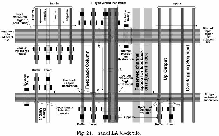
36 LOGIC ARCHITECTURE Figure shows a simple Programmable Logic Array (PLA) built using the building blocks
37 LOGIC ARCHITECTURE Two interconnected logic planes,, Each plane is composed of a programmable wired-or array, followed by a restoration array Two restoration arrays: one providing the inverted sense of the OR-term logic and one providing the non-inverted buffered sense The entire construction is a set of crossed NWs as allowed by assembly constraints The logic gates in each plane are composed of a diode-programmable wired-or NW, followed by a field-effect effect buffer or inverter NW
38 LOGIC ARCHITECTURE
39 LOGIC ARCHITECTURE Basic Clocking The basic nanopla is simply two restoring logic stages back-to to-back If we turn off all three of the control transistors in restoring stages, there is no current path from the input to the diode output stage The output stage is capacitively loaded, so it will hold its value This is the same strategy as two-phase clocking in conventional VLSI
40 LOGIC ARCHITECTURE Interconnect We know from VLSI that large PLAs do not always allow us to exploit the structure which exists in logic limitation on NW length bounds the size of the PLAs we can reasonably build to scale up to large capacity logic devices, we must interconnect modest size nanopla blocks The key idea for interconnecting nanopla blocks is to overlap the restored output NWs from each such block with the wired-or input region of adjacent nanopla blocks
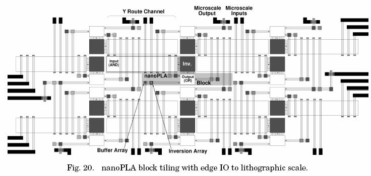
41 LOGIC ARCHITECTURE
42 LOGIC ARCHITECTURE

43 CMOS IO LOGIC ARCHITECTURE NanoPLAs will be built on top of a lithographic substrate Lithographic circuitry and wiring provides a way to probe the NWs,, to map their defects and to configure the logic we can provide IO blocks to connect the nanoscale logic to lithographic-scale
44 DEFECT TOLERANCE Small percentage of wires are defective and crosspoints are nonprogrammable Due to stochastic assembly and misalignment a percentage of NWs are unusable We can provide spare NWs in an array, test NWs for usability, and configure the array using only the non-defective NWs NW Sparing The probability of having exactly i restored OR-terms is:
45 DEFECT TOLERANCE Probability of having at least M non-defective wires out of N:
46 BOOTSTRAP TESTING Discovery we will need to discover the live addresses and their restoration polarity We must identify which NWs are usable and which are not Programming To program any diode crosspoint,, we drive one address into the top address decoder and the second into the bottom We effectively place the desired programming voltage differential across a single crosspoint

47 BOOTSTRAP TESTING Programming Diode Crosspoints Knowing which polarities are available from each of the present addresses, we can program up the intended function
48 CAD MAPPING To map from standard logic netlists (e.g., BLIF) to the nanopla arrays, a combination of conventional and custom tools as shown in the figure are used
49 CAD MAPPING SIS performs standard technology independent optimizations and decomposes the logic into small fanin nodes for covering. PLAMAP covers the logic into (I,P,O) PLA clusters These clusters can then be placed with VPR We developed our own nanopla router (npr( npr) for routing
50 COST MODELS Text presents estimations and calculations for area and delay of the proposed architecture It also gives formulas for NW capacitance and resistance Power and energy relations are also given
51 Key NanoPLA parameters Wseg is the number of NWs in each output group Lseg is the number of nanopla block heights up or down which each output Crosses F is the number of NWs in the feedback group P is the number of logical PTERMS in the input (AND) plane of the nanopla logic block Op is the number of total outputs in the OR plane Pp is the number of total PTERMS in the input (AND) plane Since these are also used for route-through connections, this is larger than the number of logical PTERMS in each logic block: Pp P + 2 Wseg + F
52 DESIGN SPACE EXPLORATION
53 DESIGN SPACE EXPLORATION Stochastic vs. Deterministic Construction.
54 DESIGN SPACE EXPLORATION Feature Sizes. Figure shows the impact of lithographic support technology and reduced diode pitch.
55 DESIGN SPACE EXPLORATION NW Lengths: Figure shows the lengths of the key NW features
56 DESIGN SPACE EXPLORATION Delay
57 DESIGN SPACE EXPLORATION Power Density
CSCI 2570 Introduction to Nanocomputing
 CSCI 2570 Introduction to Nanocomputing Introduction to NW Decoders John E Savage Lecture Outline Growing nanowires (NWs) Crossbar-based computing Types of NW decoders Resistive model of decoders Addressing
PREVIOUS work (e.g., [1], [2]) has demonstrated that it is
![PREVIOUS work (e.g., [1], [2]) has demonstrated that it is](/thumbs/77/75410442.jpg "PREVIOUS work (e.g., [1], [2]) has demonstrated that it is") IEEE TRANSACTIONS ON NANOTECHNOLOGY, VOL. 4, NO. 6, NOVEMBER 2005 681 Deterministic Addressing of Nanoscale Devices Assembled at Sublithographic Pitches André DeHon, Member, IEEE Abstract Multiple techniques
IEEE TRANSACTIONS ON NANOTECHNOLOGY, VOL. 4, NO. 6, NOVEMBER 2005 681 Deterministic Addressing of Nanoscale Devices Assembled at Sublithographic Pitches André DeHon, Member, IEEE Abstract Multiple techniques
NanoFabrics: : Spatial Computing Using Molecular Electronics
 NanoFabrics: : Spatial Computing Using Molecular Electronics Seth Copen Goldstein and Mihai Budiu Computer Architecture, 2001. Proceedings. 28th Annual International Symposium on 30 June-4 4 July 2001
Stochastic Assembly of Sublithographic Nanoscale Interfaces
 IEEE TRANSACTIONS ON NANOTECHNOLOGY, VOL. 2, NO. 3, SEPTEMBER 2003 165 Stochastic Assembly of Sublithographic Nanoscale Interfaces André DeHon, Member, IEEE, Patrick Lincoln, and John E. Savage, Life Fellow,
Evaluating Area and Performance of Hybrid FPGAs with Nanoscale Clusters and CMOS Routing
 Evaluating Area and Performance of Hybrid FPGAs with Nanoscale Clusters and CMOS Routing REZA M.P. RAD University of Maryland and MOHAMMAD TEHRANIPOOR University of Connecticut Advances in fabrication
Variation and Defect Tolerance for Nano Crossbars. Cihan Tunc
 Variation and Defect Tolerance for Nano Crossbars A Thesis Presented by Cihan Tunc to The Department of Electrical and Computer Engineering in partial fulfillment of the requirements for the degree of
2009 Spring CS211 Digital Systems & Lab 1 CHAPTER 3: TECHNOLOGY (PART 2)
") 1 CHAPTER 3: IMPLEMENTATION TECHNOLOGY (PART 2) Whatwillwelearninthischapter? we learn in this 2 How transistors operate and form simple switches CMOS logic gates IC technology FPGAs and other PLDs Basic
1 CHAPTER 3: IMPLEMENTATION TECHNOLOGY (PART 2) Whatwillwelearninthischapter? we learn in this 2 How transistors operate and form simple switches CMOS logic gates IC technology FPGAs and other PLDs Basic
Robust Nanowire Decoding
 Robust Nanowire Decoding Eric Rachlin Abstract In recent years, a number of nanoscale devices have been demonstrated that act as wires and gates. In theory, these devices can interconnect to form general
Algorithms and Techniques for Conquering Extreme Physical Variation in Bottom-Up Nanoscale Systems
 Algorithms and Techniques for Conquering Extreme Physical Variation in Bottom-Up Nanoscale Systems Thesis by Benjamin Gojman In Partial Fulfillment of the Requirements for the Degree of Master of Science
FIELD-PROGRAMMABLE gate array (FPGA) chips
 chips") IEEE TRANSACTIONS ON CIRCUITS AND SYSTEMS I: REGULAR PAPERS, VOL. 54, NO. 11, NOVEMBER 2007 2489 3-D nfpga: A Reconfigurable Architecture for 3-D CMOS/Nanomaterial Hybrid Digital Circuits Chen Dong, Deming
IEEE TRANSACTIONS ON CIRCUITS AND SYSTEMS I: REGULAR PAPERS, VOL. 54, NO. 11, NOVEMBER 2007 2489 3-D nfpga: A Reconfigurable Architecture for 3-D CMOS/Nanomaterial Hybrid Digital Circuits Chen Dong, Deming
Lecture 12 Memory Circuits. Memory Architecture: Decoders. Semiconductor Memory Classification. Array-Structured Memory Architecture RWM NVRWM ROM
 Semiconductor Memory Classification Lecture 12 Memory Circuits RWM NVRWM ROM Peter Cheung Department of Electrical & Electronic Engineering Imperial College London Reading: Weste Ch 8.3.1-8.3.2, Rabaey
Array-Based Architecture for FET-Based, Nanoscale Electronics
 IEEE TRANSACTIONS ON NANOTECHNOLOGY, VOL. 2, NO. 1, MARCH 2003 23 Array-Based Architecture for FET-Based, Nanoscale Electronics André DeHon, Member, IEEE Abstract Advances in our basic scientific understanding
+1 (479)
") Introduction to VLSI Design http://csce.uark.edu +1 (479) 575-6043 yrpeng@uark.edu Invention of the Transistor Vacuum tubes ruled in first half of 20th century Large, expensive, power-hungry, unreliable
Introduction to VLSI Design http://csce.uark.edu +1 (479) 575-6043 yrpeng@uark.edu Invention of the Transistor Vacuum tubes ruled in first half of 20th century Large, expensive, power-hungry, unreliable
Computing with nanoscale devices -- looking at alternate models
 Oregon Health & Science University OHSU Digital Commons Scholar Archive May 2005 Computing with nanoscale devices -- looking at alternate models Karthikeyan VijayaRamachandran Follow this and additional
Novel Devices and Circuits for Computing
 Novel Devices and Circuits for Computing UCSB 594BB Winter 2013 Lecture 7: CMOL Outline CMOL Main idea 3D CMOL CMOL memory CMOL logic General purporse Threshold logic Pattern matching Hybrid CMOS/Memristor
Application-Independent Defect-Tolerant Crossbar Nano-Architectures
 Application-Independent Defect-Tolerant Crossbar Nano-Architectures Mehdi B. Tahoori Electrical & Computer Engineering Northeastern University Boston, MA mtahoori@ece.neu.edu ABSTRACT Defect tolerance
EC 1354-Principles of VLSI Design
 EC 1354-Principles of VLSI Design UNIT I MOS TRANSISTOR THEORY AND PROCESS TECHNOLOGY PART-A 1. What are the four generations of integrated circuits? 2. Give the advantages of IC. 3. Give the variety of
CMPEN 411 VLSI Digital Circuits Spring Lecture 24: Peripheral Memory Circuits
 CMPEN 411 VLSI Digital Circuits Spring 2011 Lecture 24: Peripheral Memory Circuits [Adapted from Rabaey s Digital Integrated Circuits, Second Edition, 2003 J. Rabaey, A. Chandrakasan, B. Nikolic] Sp11
CSCI 2570 Introduction to Nanocomputing
 CSCI 2570 Introduction to Nanocomputing Encoded NW Decoders John E Savage Lecture Outline Encoded NW Decoders Axial and radial encoding Addressing Strategies All different, Most different, All present,
Very Large Scale Integration (VLSI)
") Very Large Scale Integration (VLSI) Lecture 6 Dr. Ahmed H. Madian Ah_madian@hotmail.com Dr. Ahmed H. Madian-VLSI 1 Contents Array subsystems Gate arrays technology Sea-of-gates Standard cell Macrocell
Very Large Scale Integration (VLSI) Lecture 6 Dr. Ahmed H. Madian Ah_madian@hotmail.com Dr. Ahmed H. Madian-VLSI 1 Contents Array subsystems Gate arrays technology Sea-of-gates Standard cell Macrocell
Preface to Third Edition Deep Submicron Digital IC Design p. 1 Introduction p. 1 Brief History of IC Industry p. 3 Review of Digital Logic Gate
 Preface to Third Edition p. xiii Deep Submicron Digital IC Design p. 1 Introduction p. 1 Brief History of IC Industry p. 3 Review of Digital Logic Gate Design p. 6 Basic Logic Functions p. 6 Implementation
Efficient logic architectures for CMOL nanoelectronic circuits
 Efficient logic architectures for CMOL nanoelectronic circuits C. Dong, W. Wang and S. Haruehanroengra Abstract: CMOS molecular (CMOL) circuits promise great opportunities for future hybrid nanoscale IC
PHYSICAL STRUCTURE OF CMOS INTEGRATED CIRCUITS. Dr. Mohammed M. Farag
 PHYSICAL STRUCTURE OF CMOS INTEGRATED CIRCUITS Dr. Mohammed M. Farag Outline Integrated Circuit Layers MOSFETs CMOS Layers Designing FET Arrays EE 432 VLSI Modeling and Design 2 Integrated Circuit Layers
Introduction to CMOS VLSI Design (E158) Lecture 9: Cell Design
 Lecture 9: Cell Design") Harris Introduction to CMOS VLSI Design (E158) Lecture 9: Cell Design David Harris Harvey Mudd College David_Harris@hmc.edu Based on EE271 developed by Mark Horowitz, Stanford University MAH E158 Lecture
Harris Introduction to CMOS VLSI Design (E158) Lecture 9: Cell Design David Harris Harvey Mudd College David_Harris@hmc.edu Based on EE271 developed by Mark Horowitz, Stanford University MAH E158 Lecture
Lecture 9: Cell Design Issues
 Lecture 9: Cell Design Issues MAH, AEN EE271 Lecture 9 1 Overview Reading W&E 6.3 to 6.3.6 - FPGA, Gate Array, and Std Cell design W&E 5.3 - Cell design Introduction This lecture will look at some of the
Transistor was first invented by William.B.Shockley, Walter Brattain and John Bardeen of Bell Labratories. In 1961, first IC was introduced.
 Unit 1 Basic MOS Technology Transistor was first invented by William.B.Shockley, Walter Brattain and John Bardeen of Bell Labratories. In 1961, first IC was introduced. Levels of Integration:- i) SSI:-
Engr354: Digital Logic Circuits
 Engr354: Digital Logic Circuits Chapter 3: Implementation Technology Curtis Nelson Chapter 3 Overview In this chapter you will learn about: How transistors are used as switches; Integrated circuit technology;
Fault-Tolerant Nanoscale Processors on Semiconductor Nanowire Grids
 Fault-Tolerant Nanoscale Processors on Semiconductor Nanowire Grids Csaba Andras Moritz, Teng Wang, Pritish Narayanan, Michael Leuchtenburg, Yao Guo, Catherine Dezan, and Mahmoud Bennaser Abstract Nanoscale
Fault Tolerance in VLSI Systems
 Fault Tolerance in VLSI Systems Overview Opportunities presented by VLSI Problems presented by VLSI Redundancy techniques in VLSI design environment Duplication with complementary logic Self-checking logic
Yet, many signal processing systems require both digital and analog circuits. To enable
 Introduction Field-Programmable Gate Arrays (FPGAs) have been a superb solution for rapid and reliable prototyping of digital logic systems at low cost for more than twenty years. Yet, many signal processing
Array-Based Architecture for Molecular Electronics
 Array-Based Architecture for Molecular Electronics André DeHon Department of Computer Science, 256-80 California Institute of Technology Pasadena, CA 91125 andre@acm.org Abstract Microscale Wiring NT/NW
1 Introduction
 Published in Micro & Nano Letters Received on 9th April 2008 Revised on 27th May 2008 ISSN 1750-0443 Design of a transmission gate based CMOL memory array Z. Abid M. Barua A. Alma aitah Department of Electrical
White Paper Stratix III Programmable Power
 Introduction White Paper Stratix III Programmable Power Traditionally, digital logic has not consumed significant static power, but this has changed with very small process nodes. Leakage current in digital
Low Power System-On-Chip-Design Chapter 12: Physical Libraries
 1 Low Power System-On-Chip-Design Chapter 12: Physical Libraries Friedemann Wesner 2 Outline Standard Cell Libraries Modeling of Standard Cell Libraries Isolation Cells Level Shifters Memories Power Gating
In this lecture we will begin a new topic namely the Metal-Oxide-Semiconductor Field Effect Transistor.
 Solid State Devices Dr. S. Karmalkar Department of Electronics and Communication Engineering Indian Institute of Technology, Madras Lecture - 38 MOS Field Effect Transistor In this lecture we will begin
EE 42/100 Lecture 23: CMOS Transistors and Logic Gates. Rev A 4/15/2012 (10:39 AM) Prof. Ali M. Niknejad
 Prof. Ali M. Niknejad") A. M. Niknejad University of California, Berkeley EE 100 / 42 Lecture 23 p. 1/16 EE 42/100 Lecture 23: CMOS Transistors and Logic Gates ELECTRONICS Rev A 4/15/2012 (10:39 AM) Prof. Ali M. Niknejad University
A. M. Niknejad University of California, Berkeley EE 100 / 42 Lecture 23 p. 1/16 EE 42/100 Lecture 23: CMOS Transistors and Logic Gates ELECTRONICS Rev A 4/15/2012 (10:39 AM) Prof. Ali M. Niknejad University
Product Information. Allegro Hall-Effect Sensor ICs. By Shaun Milano Allegro MicroSystems, LLC. Hall Effect Principles. Lorentz Force F = q v B V = 0
 Product Information Allegro Hall-Effect Sensor ICs y Shaun Milano Allegro MicroSystems, LLC is a world leader in developing, manufacturing, and marketing high-performance Halleffect sensor integrated circuits.
Defect Tolerance in VLSI Circuits: Techniques and Yield Analysis
 Defect Tolerance in VLSI Circuits: Techniques and Yield Analysis ISRAEL KOREN, FELLOW, IEEE, and ZAHAVA KOREN Current very-large-scale-integration (VLSI) technology allows the manufacture of large-area
EE301 Electronics I , Fall
 EE301 Electronics I 2018-2019, Fall 1. Introduction to Microelectronics (1 Week/3 Hrs.) Introduction, Historical Background, Basic Consepts 2. Rewiev of Semiconductors (1 Week/3 Hrs.) Semiconductor materials
Power Optimization of FPGA Interconnect Via Circuit and CAD Techniques
 Power Optimization of FPGA Interconnect Via Circuit and CAD Techniques Safeen Huda and Jason Anderson International Symposium on Physical Design Santa Rosa, CA, April 6, 2016 1 Motivation FPGA power increasingly
ECE380 Digital Logic
 ECE380 Digital Logic Implementation Technology: Standard Chips and Programmable Logic Devices Dr. D. J. Jackson Lecture 10-1 Standard chips A number of chips, each with a few logic gates, are commonly
Disseny físic. Disseny en Standard Cells. Enric Pastor Rosa M. Badia Ramon Canal DM Tardor DM, Tardor
 Disseny físic Disseny en Standard Cells Enric Pastor Rosa M. Badia Ramon Canal DM Tardor 2005 DM, Tardor 2005 1 Design domains (Gajski) Structural Processor, memory ALU, registers Cell Device, gate Transistor
Reconfigurable Nano-Crossbar Architectures
 Reconfigurable Nano-Crossbar Architectures Dmitri B. Strukov, Department of Electrical and Computer Engineering, University of Santa Barbara, USA Konstantin K. Likharev, Department of Physics and Astronomy,
Reference. Wayne Wolf, FPGA-Based System Design Pearson Education, N Krishna Prakash,, Amrita School of Engineering
 FPGA Fabrics Reference Wayne Wolf, FPGA-Based System Design Pearson Education, 2004 CPLD / FPGA CPLD Interconnection of several PLD blocks with Programmable interconnect on a single chip Logic blocks executes
Memory Basics. historically defined as memory array with individual bit access refers to memory with both Read and Write capabilities
 Memory Basics RAM: Random Access Memory historically defined as memory array with individual bit access refers to memory with both Read and Write capabilities ROM: Read Only Memory no capabilities for
Methodologies for Tolerating Cell and Interconnect Faults in FPGAs
 IEEE TRANSACTIONS ON COMPUTERS, VOL. 47, NO. 1, JANUARY 1998 15 Methodologies for Tolerating Cell and Interconnect Faults in FPGAs Fran Hanchek, Member, IEEE, and Shantanu Dutt, Member, IEEE Abstract The
Jack Keil Wolf Lecture. ESE 570: Digital Integrated Circuits and VLSI Fundamentals. Lecture Outline. MOSFET N-Type, P-Type.
 ESE 570: Digital Integrated Circuits and VLSI Fundamentals Jack Keil Wolf Lecture Lec 3: January 24, 2019 MOS Fabrication pt. 2: Design Rules and Layout http://www.ese.upenn.edu/about-ese/events/wolf.php
Topics. Memory Reliability and Yield Control Logic. John A. Chandy Dept. of Electrical and Computer Engineering University of Connecticut
 Topics Memory Reliability and Yield Control Logic Reliability and Yield Noise Sources in T DRam BL substrate Adjacent BL C WBL α-particles WL leakage C S electrode C cross Transposed-Bitline Architecture
Interconnect. Physical Entities
 Interconnect André DeHon Thursday, June 20, 2002 Physical Entities Idea: Computations take up space Bigger/smaller computations Size resources cost Size distance delay 1 Impact Consequence
LSI Design Flow Development for Advanced Technology
 LSI Design Flow Development for Advanced Technology Atsushi Tsuchiya LSIs that adopt advanced technologies, as represented by imaging LSIs, now contain 30 million or more logic gates and the scale is beginning
Investigating the Electronic Behavior of Nano-materials From Charge Transport Properties to System Response
 Investigating the Electronic Behavior of Nano-materials From Charge Transport Properties to System Response Amit Verma Assistant Professor Department of Electrical Engineering & Computer Science Texas
A Case Study of Nanoscale FPGA Programmable Switches with Low Power
 A Case Study of Nanoscale FPGA Programmable Switches with Low Power V.Elamaran 1, Har Narayan Upadhyay 2 1 Assistant Professor, Department of ECE, School of EEE SASTRA University, Tamilnadu - 613401, India
In pursuit of high-density storage class memory
 Edition October 2017 Semiconductor technology & processing In pursuit of high-density storage class memory A novel thermally stable GeSe-based selector paves the way to storage class memory applications.
ESE 570: Digital Integrated Circuits and VLSI Fundamentals
 ESE 570: Digital Integrated Circuits and VLSI Fundamentals Lec 3: January 24, 2019 MOS Fabrication pt. 2: Design Rules and Layout Penn ESE 570 Spring 2019 Khanna Jack Keil Wolf Lecture http://www.ese.upenn.edu/about-ese/events/wolf.php
Lecture #2 Solving the Interconnect Problems in VLSI
 Lecture #2 Solving the Interconnect Problems in VLSI C.P. Ravikumar IIT Madras - C.P. Ravikumar 1 Interconnect Problems Interconnect delay has become more important than gate delays after 130nm technology
Chapter 3 Chip Planning
 Chapter 3 Chip Planning 3.1 Introduction to Floorplanning 3. Optimization Goals in Floorplanning 3.3 Terminology 3.4 Floorplan Representations 3.4.1 Floorplan to a Constraint-Graph Pair 3.4. Floorplan
Layers. Layers. Layers. Transistor Manufacturing COMP375 1
 Layers VLSI COMP370 Intro to Computer Architecture t Applications Middleware other CS classes High level languages Machine Language Microcode Logic circuits Gates Transistors Silicon structures Layers
Difference between BJTs and FETs. Junction Field Effect Transistors (JFET)
") Difference between BJTs and FETs Transistors can be categorized according to their structure, and two of the more commonly known transistor structures, are the BJT and FET. The comparison between BJTs
Difference between BJTs and FETs Transistors can be categorized according to their structure, and two of the more commonly known transistor structures, are the BJT and FET. The comparison between BJTs
Advanced Digital Design
 Advanced Digital Design Introduction & Motivation by A. Steininger and M. Delvai Vienna University of Technology Outline Challenges in Digital Design The Role of Time in the Design The Fundamental Design
MTLE-6120: Advanced Electronic Properties of Materials. Semiconductor transistors for logic and memory. Reading: Kasap
 MTLE-6120: Advanced Electronic Properties of Materials 1 Semiconductor transistors for logic and memory Reading: Kasap 6.6-6.8 Vacuum tube diodes 2 Thermionic emission from cathode Electrons collected
UNIT-II LOW POWER VLSI DESIGN APPROACHES
 UNIT-II LOW POWER VLSI DESIGN APPROACHES Low power Design through Voltage Scaling: The switching power dissipation in CMOS digital integrated circuits is a strong function of the power supply voltage.
Atoms and Valence Electrons
 Technology Overview Atoms and Valence Electrons Conduc:on and Valence Bands Energy Band Gaps in Materials Band gap N- type and P- type Doping Silicon and Adjacent Atoms PN Junc:on Forward Biased PN Junc:on
Basic Functional Analysis. Sample Report Richmond Road, Suite 500, Ottawa, ON K2H 5B7 Canada Tel:
 Basic Functional Analysis Sample Report 3685 Richmond Road, Suite 500, Ottawa, ON K2H 5B7 Canada Tel: 613-829-0414 www.chipworks.com Basic Functional Analysis Sample Report Some of the information in this
Power-Delivery Network in 3D ICs: Monolithic 3D vs. Skybridge 3D CMOS
 -Delivery Network in 3D ICs: Monolithic 3D vs. Skybridge 3D CMOS Jiajun Shi, Mingyu Li and Csaba Andras Moritz Department of Electrical and Computer Engineering University of Massachusetts, Amherst, MA,
TECHNO INDIA BATANAGAR (DEPARTMENT OF ELECTRONICS & COMMUNICATION ENGINEERING) QUESTION BANK- 2018
 QUESTION BANK- 2018") TECHNO INDIA BATANAGAR (DEPARTMENT OF ELECTRONICS & COMMUNICATION ENGINEERING) QUESTION BANK- 2018 Paper Setter Detail Name Designation Mobile No. E-mail ID Raina Modak Assistant Professor 6290025725 raina.modak@tib.edu.in
TECHNO INDIA BATANAGAR (DEPARTMENT OF ELECTRONICS & COMMUNICATION ENGINEERING) QUESTION BANK- 2018 Paper Setter Detail Name Designation Mobile No. E-mail ID Raina Modak Assistant Professor 6290025725 raina.modak@tib.edu.in
Layers. Layers. Layers. Transistor Manufacturing COMP375 1
 VLSI COMP375 Computer Architecture Middleware other CS classes Machine Language Microcode Logic circuits Transistors Middleware Machine Language - earlier Microcode Logic circuits Transistors Middleware
Field Effect Transistors (npn)
") Field Effect Transistors (npn) gate drain source FET 3 terminal device channel e - current from source to drain controlled by the electric field generated by the gate base collector emitter BJT 3 terminal
Field Effect Transistors (npn) gate drain source FET 3 terminal device channel e - current from source to drain controlled by the electric field generated by the gate base collector emitter BJT 3 terminal
ECE 5745 Complex Digital ASIC Design Topic 2: CMOS Devices
 ECE 5745 Complex Digital ASIC Design Topic 2: CMOS Devices Christopher Batten School of Electrical and Computer Engineering Cornell University http://www.csl.cornell.edu/courses/ece5950 Simple Transistor
PROGRAMMABLE ASIC INTERCONNECT
 PROGRAMMABLE ASIC INTERCONNECT The structure and complexity of the interconnect is largely determined by the programming technology and the architecture of the basic logic cell The first programmable ASICs
Towards PVT-Tolerant Glitch-Free Operation in FPGAs
 Towards PVT-Tolerant Glitch-Free Operation in FPGAs Safeen Huda and Jason H. Anderson ECE Department, University of Toronto, Canada 24 th ACM/SIGDA International Symposium on FPGAs February 22, 2016 Motivation
(Refer Slide Time: 02:05)
") Electronics for Analog Signal Processing - I Prof. K. Radhakrishna Rao Department of Electrical Engineering Indian Institute of Technology Madras Lecture 27 Construction of a MOSFET (Refer Slide Time:
Electronics for Analog Signal Processing - I Prof. K. Radhakrishna Rao Department of Electrical Engineering Indian Institute of Technology Madras Lecture 27 Construction of a MOSFET (Refer Slide Time:
Electronic Circuits EE359A
 Electronic Circuits EE359A Bruce McNair B206 bmcnair@stevens.edu 201-216-5549 1 Memory and Advanced Digital Circuits - 2 Chapter 11 2 Figure 11.1 (a) Basic latch. (b) The latch with the feedback loop opened.
55:041 Electronic Circuits
 55:041 Electronic Circuits Mosfet Review Sections of Chapter 3 &4 A. Kruger Mosfet Review, Page-1 Basic Structure of MOS Capacitor Sect. 3.1 Width 1 10-6 m or less Thickness 50 10-9 m or less ` MOS Metal-Oxide-Semiconductor
ECE/CoE 0132: FETs and Gates
 ECE/CoE 0132: FETs and Gates Kartik Mohanram September 6, 2017 1 Physical properties of gates Over the next 2 lectures, we will discuss some of the physical characteristics of integrated circuits. We will
Exploring Technology Alternatives for Nano-Scale FPGA Interconnects
 Exploring Technology Alternatives for Nano-Scale FPGA Interconnects 54.3 Aman Gayasen, N. Vijaykrishnan, M. J. Irwin Penn State University University Park {gayasen, vijay, mji}@cse.psu.edu ABSTRACT Field
A Study of Asynchronous Design Methodology for Robust CMOS-Nano Hybrid System Design
 12 A Study of Asynchronous Design Methodology for Robust CMOS-Nano Hybrid System Design RAJAT SUBHRA CHAKRABORTY and SWARUP BHUNIA Case Western Reserve University Among the emerging alternatives to CMOS,
Exhibit 2 Declaration of Dr. Chris Mack
 STC.UNM v. Intel Corporation Doc. 113 Att. 5 Exhibit 2 Declaration of Dr. Chris Mack Dockets.Justia.com UNITED STATES DISTRICT COURT DISTRICT OF NEW MEXICO STC.UNM, Plaintiff, v. INTEL CORPORATION Civil
Lecture 0: Introduction
 Lecture 0: Introduction Introduction Integrated circuits: many transistors on one chip. Very Large Scale Integration (VLSI): bucketloads! Complementary Metal Oxide Semiconductor Fast, cheap, low power
EE141-Spring 2007 Digital Integrated Circuits
 EE141-Spring 2007 Digital Integrated Circuits Lecture 22 I/O, Power Distribution dders 1 nnouncements Homework 9 has been posted Due Tu. pr. 24, 5pm Project Phase 4 (Final) Report due Mo. pr. 30, noon
Architecting Connectivity for Fine-grained 3-D Vertically Integrated Circuits
 Architecting Connectivity for Fine-grained 3-D Vertically Integrated Circuits Santosh Khasanvis, Mostafizur Rahman, Mingyu Li, Jiajun Shi, and Csaba Andras Moritz* Dept. of Electrical and Computer Engineering,
Lesson 5. Electronics: Semiconductors Doping p-n Junction Diode Half Wave and Full Wave Rectification Introduction to Transistors-
 Lesson 5 Electronics: Semiconductors Doping p-n Junction Diode Half Wave and Full Wave Rectification Introduction to Transistors- Types and Connections Semiconductors Semiconductors If there are many free
Semiconductors, ICs and Digital Fundamentals
 Semiconductors, ICs and Digital Fundamentals The Diode The semiconductor phenomena. Diode performance with ac and dc currents. Diode types: General purpose LED Zener The Diode The semiconductor phenomena
Combining 2-level Logic Families in Grid-based Nanoscale Fabrics
 Combining 2-level Logic Families in Grid-based Nanoscale Fabrics Teng Wang, Pritish Narayanan, and Csaba Andras Moritz Department of Electrical and Computer Engineering University of Massachusetts Amherst
ECE520 VLSI Design. Lecture 2: Basic MOS Physics. Payman Zarkesh-Ha
 ECE520 VLSI Design Lecture 2: Basic MOS Physics Payman Zarkesh-Ha Office: ECE Bldg. 230B Office hours: Wednesday 2:00-3:00PM or by appointment E-mail: pzarkesh@unm.edu Slide: 1 Review of Last Lecture Semiconductor
Lecture 11: Clocking
 High Speed CMOS VLSI Design Lecture 11: Clocking (c) 1997 David Harris 1.0 Introduction We have seen that generating and distributing clocks with little skew is essential to high speed circuit design.
User2User The 2007 Mentor Graphics International User Conference
 7/2/2007 1 Designing High Speed Printed Circuit Boards Using DxDesigner and Expedition Robert Navarro Jet Propulsion Laboratory, California Institute of Technology. User2User The 2007 Mentor Graphics International
I/O Design EE141. Announcements. EE141-Fall 2006 Digital Integrated Circuits. Class Material. Pads + ESD Protection.
 EE141-Fall 2006 Digital Integrated Circuits nnouncements Homework 9 due on Thursday Lecture 26 I/O 1 2 Class Material Last lecture Timing Clock distribution Today s lecture I/O Power distribution Intro
Evaluation of Low-Leakage Design Techniques for Field Programmable Gate Arrays
 Evaluation of Low-Leakage Design Techniques for Field Programmable Gate Arrays Arifur Rahman and Vijay Polavarapuv Department of Electrical and Computer Engineering, Polytechnic University, Brooklyn, NY
ALPS: An Automatic Layouter for Pass-Transistor Cell Synthesis
 ALPS: An Automatic Layouter for Pass-Transistor Cell Synthesis Yasuhiko Sasaki Central Research Laboratory Hitachi, Ltd. Kokubunji, Tokyo, 185, Japan Kunihito Rikino Hitachi Device Engineering Kokubunji,
Leakage Power Modeling and Reduction Techniques for Field Programmable Gate Arrays
 Leakage Power Modeling and Reduction Techniques for Field Programmable Gate Arrays by Akhilesh Kumar A thesis presented to the University of Waterloo in fulfilment of the thesis requirement for the degree
Number of Lessons:155 #14B (P) Electronics Technology with Digital and Microprocessor Laboratory Completion Time: 42 months
 Electronics Technology with Digital and Microprocessor Laboratory Completion Time: 42 months") PROGRESS RECORD Study your lessons in the order listed below. Number of Lessons:155 #14B (P) Electronics Technology with Digital and Microprocessor Laboratory Completion Time: 42 months 1 2330A Current
PROGRESS RECORD Study your lessons in the order listed below. Number of Lessons:155 #14B (P) Electronics Technology with Digital and Microprocessor Laboratory Completion Time: 42 months 1 2330A Current
ECE 340 Lecture 37 : Metal- Insulator-Semiconductor FET Class Outline:
 ECE 340 Lecture 37 : Metal- Insulator-Semiconductor FET Class Outline: Metal-Semiconductor Junctions MOSFET Basic Operation MOS Capacitor Things you should know when you leave Key Questions What is the
Integrated Circuit: Classification:
 Integrated Circuit: It is a miniature, low cost electronic circuit consisting of active and passive components that are irreparably joined together on a single crystal chip of silicon. Classification:
Effects of grid-placed contacts on circuit performance
 Title Effects of grid-placed contacts on circuit performance Author(s) Wang, J; Wong, AKK Citation Cost and Performance in Integrated Circuit Creation, Santa Clara, California, USA, 27-28 February 2003,
FABRICATION OF CMOS INTEGRATED CIRCUITS. Dr. Mohammed M. Farag
 FABRICATION OF CMOS INTEGRATED CIRCUITS Dr. Mohammed M. Farag Outline Overview of CMOS Fabrication Processes The CMOS Fabrication Process Flow Design Rules Reference: Uyemura, John P. "Introduction to
Trends and Challenges in VLSI Technology Scaling Towards 100nm
 Trends and Challenges in VLSI Technology Scaling Towards 100nm Stefan Rusu Intel Corporation stefan.rusu@intel.com September 2001 Stefan Rusu 9/2001 2001 Intel Corp. Page 1 Agenda VLSI Technology Trends
Nanoscale Molecular-Switch Crossbar Circuits
 Nanoscale Molecular-Switch Crossbar Circuits Sung Hyun Jo Ph.D. Student, Dept. of Electrical Engineering & Computer Science Ken Loh Ph.D. Student, Dept. of Civil & Environmental Engineering EECS 598 Nanoelectronics
SUPPLEMENTARY INFORMATION
 SUPPLEMENTARY INFORMATION Dopant profiling and surface analysis of silicon nanowires using capacitance-voltage measurements Erik C. Garnett 1, Yu-Chih Tseng 4, Devesh Khanal 2,3, Junqiao Wu 2,3, Jeffrey
Low Power Multiplier Design Using Complementary Pass-Transistor Asynchronous Adiabatic Logic
 Low Power Multiplier Design Using Complementary Pass-Transistor Asynchronous Adiabatic Logic A.Kishore Kumar 1 Dr.D.Somasundareswari 2 Dr.V.Duraisamy 3 M.Pradeepkumar 4 1 Lecturer-Department of ECE, 3
ESE370: Circuit-Level Modeling, Design, and Optimization for Digital Systems. Today. Variation. Variation. Process Corners.
 ESE370: Circuit-Level Modeling, Design, and Optimization for Digital Systems Day 13: October 3, 2012 Layout and Area Today Coping with Variation (from last time) Layout Transistors Gates Design rules Standard