PAD: Procedural Analog Design Tool D. Stefanovic, M. Kayal, M. Pastre
|
|
|
- Amanda Logan
- 6 years ago
- Views:
Transcription
1 PAD: Procedural Analog Design Tool D. Stefanovic, M. Kayal, M. Pastre Swiss Federal Institute of Technology, Electronic Labs, STI/IMM/LEG, Lausanne, Switzerland
2 Procedural Analog Design Tool Interactive chart-based tool Dedicated to step-by-step design of analog cells The present version covers the design of: basic analog structures procedural design of OTAs and different operational amplifiers topologies (complex analog structures) Transistor-level calculator embedded in PAD uses the complete set of equations of the EKV MOS model
3 Top down system design approach Digital Behavioral modeling and simulation Analog PAD tool Behavioral simulation and synthesis Specs of basic blocks Circuit schematic Layout generation, extraction and post layout simulation Transistor sizing Layout generation, extraction and post layout simulation Assembling
4 Combine approaches: PAD tool Analog Structures Sizing and Layout Generation Procedural Design of Complex Analog structures top-down High Level Behavioural System simulation (VHDL_AMS, VerilogA,...) System On Chip Complete design methodology, from system-level to transistor-level bottom-up Structured Transistor-level Design of Analog Cells Analog structures library, Procedural design methodology


5 PAD structure

6 The charts!
7 EKV MOS model Transistor level calculator dedicated to the design of analog circuits based on device physics links weak and strong inversion in a continuous way has small number of model parameters, but good accuracy solutions for different input parameter sets are found without using complex numerical methods large number of transistor parameters can be extracted
8 Analog structures library single transistor current mirror cascode current mirror differential pair cascode stage folded cascode stage common source common drain general params small signal params DC biasing values parasitic capas transition frequency specific params maximum DC offset current mismatch output resistance gain
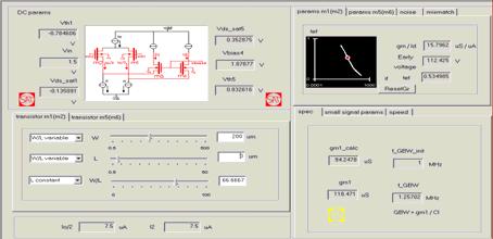
9 g m /I D design procedure set priority targets (gain, noise, speed ) choose bias current and accordingly gm/id ratio change free variables (W, L) observe effects on other parameters
10 Procedural Design of Complex Structures Circuit Partitioning Chart-Oriented Basic Analog Structures Sizing Circuit Level Performances


11 Procedural Design of Complex Structures
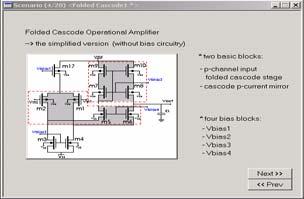
12 Procedural Design of Folded Cascode OTA V DD m20 m18 m17 m9 m10 m12 m14 V DD V DD V DD V DD V DD V DD V DD V bias1 V bias1 V bias1 m7 m8 m11 V bias3 I bias I bias I o m1 m2 V DD I 2 I 2 V DD V DD V bias4 I bias2 m15 V out m19 V bias2 V DD m3 V DD I 1 I 1 m4 V ss m5 m6 V ss V bias2 I bias1 m13 V ss m16 V DD C L V ss V ss V ss V ss V SS

13 PAD Design Flow Initialisation :
14 PAD Design Flow Circuit partitioning : I bias I bias p current mirror folded cascode pair cascode current mirror bias3 bias4 n current mirror
15 PAD Design Flow Determination of circuit currents : V DD I I o _ calc I o = SR o C L _ calc m1 I o m2 I 2 I 2 I 2 = V bias4 I 1 I o 2 V DD V DD V ss m5 m6 V ss I o I 1 n I o I 1 I 1 g _ calc = 2π f _ GBW m C L V SS
16 PAD Design Flow SR, CMR +, CMRR, PSRR + Sizing of basic analog structures : CMR -, PSRR -, noise, stability I bias I bias p current mirror folded cascode pair n current mirror gain, noise, offset, stability, output swing cascode current mirror GBW, gain, noise, offset, stability

17 Circuit level design : PAD Design Flow
18 Circuit level design : PAD Design Flow
19 Circuit level design : PAD Design Flow

20 Circuit level design : PAD Design Flow
21 Conclusion new chart-based procedural analog design tool new knowledge-based analog design methodology design and re-design of wide range of circuits didactical tool that helps to hand analog knowledge towards non-expert designer
22 Download If you have any questions:
ECEN 474/704 Lab 7: Operational Transconductance Amplifiers
 ECEN 474/704 Lab 7: Operational Transconductance Amplifiers Objective Design, simulate and layout an operational transconductance amplifier. Introduction The operational transconductance amplifier (OTA)
ECEN 474/704 Lab 6: Differential Pairs
 ECEN 474/704 Lab 6: Differential Pairs Objective Design, simulate and layout various differential pairs used in different types of differential amplifiers such as operational transconductance amplifiers
Radivoje Đurić, 2015, Analogna Integrisana Kola 1
 Low power OTA 1 Two-Stage, Miller Op Amp Operating in Weak Inversion Low frequency response: gm1 gm6 Av 0 g g g g A v 0 ds2 ds4 ds6 ds7 I D m, ds D nvt g g I n GB and SR: GB 1 1 n 1 2 4 6 6 7 g 2 2 m1
A Novel Design of Low Voltage,Wilson Current Mirror based Wideband Operational Transconductance Amplifier
 A Novel Design of Low Voltage,Wilson Current Mirror based Wideband Operational Transconductance Amplifier Kehul A. Shah 1, N.M.Devashrayee 2 1(Associative Prof., Department of Electronics and Communication,
CSE 577 Spring Insoo Kim, Kyusun Choi Mixed Signal CHIP Design Lab. Department of Computer Science & Engineering The Penn State University
 CSE 577 Spring 2011 Basic Amplifiers and Differential Amplifier, Kyusun Choi Mixed Signal CHIP Design Lab. Department of Computer Science & Engineering The Penn State University Don t let the computer
Chapter 12 Opertational Amplifier Circuits
 1 Chapter 12 Opertational Amplifier Circuits Learning Objectives 1) The design and analysis of the two basic CMOS op-amp architectures: the two-stage circuit and the single-stage, folded cascode circuit.
444 Index. F Fermi potential, 146 FGMOS transistor, 20 23, 57, 83, 84, 98, 205, 208, 213, 215, 216, 241, 242, 251, 280, 311, 318, 332, 354, 407
 Index A Accuracy active resistor structures, 46, 323, 328, 329, 341, 344, 360 computational circuits, 171 differential amplifiers, 30, 31 exponential circuits, 285, 291, 292 multifunctional structures,
IJSRD - International Journal for Scientific Research & Development Vol. 4, Issue 03, 2016 ISSN (online):
:") IJSRD - International Journal for Scientific Research & Development Vol. 4, Issue 03, 2016 ISSN (online): 2321-0613 Design and Analysis of Wide Swing Folded-Cascode OTA using 180nm Technology Priyanka
IJSRD - International Journal for Scientific Research & Development Vol. 4, Issue 03, 2016 ISSN (online): 2321-0613 Design and Analysis of Wide Swing Folded-Cascode OTA using 180nm Technology Priyanka
A Compact Folded-cascode Operational Amplifier with Class-AB Output Stage
 A Compact Folded-cascode Operational Amplifier with Class-AB Output Stage EEE 523 Advanced Analog Integrated Circuits Project Report Fuding Ge You are an engineer who is assigned the project to design
Radivoje Đurić, 2015, Analogna Integrisana Kola 1
 Rail-to to-rail OTA 1 Rail-to-rail CMOS op amp Generally, rail-to-rail amplifiers are useful in low-voltage applications, where it is necessary to efficiently use the limited span offered by the power
ECEN 474/704 Lab 8: Two-Stage Miller Operational Amplifier
 ECEN 474/704 Lab 8: Two-Stage Miller Operational Amplifier Objective Design, simulate and test a two-stage operational amplifier Introduction Operational amplifiers (opamp) are essential components of
ANALYSIS AND DESIGN OF ANALOG INTEGRATED CIRCUITS
 ANALYSIS AND DESIGN OF ANALOG INTEGRATED CIRCUITS Fourth Edition PAUL R. GRAY University of California, Berkeley PAUL J. HURST University of California, Davis STEPHEN H. LEWIS University of California,
METHODOLOGY FOR THE DIGITAL CALIBRATION OF ANALOG CIRCUITS AND SYSTEMS
 METHODOLOGY FOR THE DIGITAL CALIBRATION OF ANALOG CIRCUITS AND SYSTEMS METHODOLOGY FOR THE DIGITAL CALIBRATION OF ANALOG CIRCUITS AND SYSTEMS with Case Studies by Marc Pastre Ecole Polytechnique Fédérale
International Journal of Emerging Technologies in Computational and Applied Sciences (IJETCAS)
") International Association of Scientific Innovation and Research (IASIR) (An Association Unifying the Sciences, Engineering, and Applied Research) International Journal of Emerging Technologies in Computational
International Association of Scientific Innovation and Research (IASIR) (An Association Unifying the Sciences, Engineering, and Applied Research) International Journal of Emerging Technologies in Computational
Advanced Operational Amplifiers
 IsLab Analog Integrated Circuit Design OPA2-47 Advanced Operational Amplifiers כ Kyungpook National University IsLab Analog Integrated Circuit Design OPA2-1 Advanced Current Mirrors and Opamps Two-stage
Design of an Amplifier for Sensor Interfaces
 Design of an Amplifier for Sensor Interfaces Anurag Mangla Electrical and Electronics Engineering anurag.mangla@epfl.ch Supervised by Dr. Marc Pastre Prof. Maher Kayal Outline Introduction Need for high
ANALYSIS AND DESIGN OF ANALOG INTEGRATED CIRCUITS
 ANALYSIS AND DESIGN OF ANALOG INTEGRATED CIRCUITS Fourth Edition PAUL R. GRAY University of California, Berkeley PAUL J. HURST University of California, Davis STEPHEN H. LEWIS University of California,
Analog Integrated Circuits. Lecture 7: OpampDesign
 Analog Integrated Circuits Lecture 7: OpampDesign ELC 601 Fall 2013 Dr. Ahmed Nader Dr. Mohamed M. Aboudina anader@ieee.org maboudina@gmail.com Department of Electronics and Communications Engineering
Design of Analog and Mixed Integrated Circuits and Systems Theory Exercises
 102726 Design of nalog and Mixed Theory Exercises Francesc Serra Graells http://www.cnm.es/~pserra/uab/damics paco.serra@imb-cnm.csic.es 1 Introduction to the Design of nalog Integrated Circuits 1.1 The
Layout-Oriented Synthesis of High Performance Analog Circuits
 -Oriented Synthesis of High Performance Analog Circuits Mohamed Dessouky, Marie-Minerve Louërat Université Paris VI (55/65) Laboratoire LIP6-ASIM 4 Place Jussieu. 75252 Paris Cedex 05. France Mohamed.Dessouky@lip6.fr
[Kumar, 2(9): September, 2013] ISSN: Impact Factor: 1.852
![[Kumar, 2(9): September, 2013] ISSN: Impact Factor: 1.852](/thumbs/86/94008668.jpg "[Kumar, 2(9): September, 2013] ISSN: Impact Factor: 1.852") IJESRT INTERNATIONAL JOURNAL OF ENGINEERING SCIENCES & RESEARCH TECHNOLOGY Design and Performance analysis of Low power CMOS Op-Amp Anand Kumar Singh *1, Anuradha 2, Dr. Vijay Nath 3 *1,2 Department of
IJESRT INTERNATIONAL JOURNAL OF ENGINEERING SCIENCES & RESEARCH TECHNOLOGY Design and Performance analysis of Low power CMOS Op-Amp Anand Kumar Singh *1, Anuradha 2, Dr. Vijay Nath 3 *1,2 Department of
2. Single Stage OpAmps
 /74 2. Single Stage OpAmps Francesc Serra Graells francesc.serra.graells@uab.cat Departament de Microelectrònica i Sistemes Electrònics Universitat Autònoma de Barcelona paco.serra@imb-cnm.csic.es Integrated
EEC 210 Fall 2008 Design Project. Rajeevan Amirtharajah Dept. of Electrical and Computer Engineering University of California, Davis
 EEC 210 Fall 2008 Design Project Rajeevan Amirtharajah Dept. of Electrical and Computer Engineering University of California, Davis Issued: November 18, 2008 Due: December 5, 2008, 5:00 PM in my office.
Analysis and Design of Analog Integrated Circuits Lecture 8. Cascode Techniques
 Analysis and Design of Analog Integrated Circuits Lecture 8 Cascode Techniques Michael H. Perrott February 15, 2012 Copyright 2012 by Michael H. Perrott All rights reserved. Review of Large Signal Analysis
DAT175: Topics in Electronic System Design
 DAT175: Topics in Electronic System Design Analog Readout Circuitry for Hearing Aid in STM90nm 21 February 2010 Remzi Yagiz Mungan v1.10 1. Introduction In this project, the aim is to design an adjustable
G m /I D based Three stage Operational Amplifier Design
 G m /I D based Three stage Operational Amplifier Design Rishabh Shukla SVNIT, Surat shuklarishabh31081988@gmail.com Abstract A nested Gm-C compensated three stage Operational Amplifier is reviewed using
Analog CMOS Interface Circuits for UMSI Chip of Environmental Monitoring Microsystem
 Analog CMOS Interface Circuits for UMSI Chip of Environmental Monitoring Microsystem A report Submitted to Canopus Systems Inc. Zuhail Sainudeen and Navid Yazdi Arizona State University July 2001 1. Overview
DESIGN OF A NOVEL CURRENT MIRROR BASED DIFFERENTIAL AMPLIFIER DESIGN WITH LATCH NETWORK. Thota Keerthi* 1, Ch. Anil Kumar 2
 ISSN 2277-2685 IJESR/October 2014/ Vol-4/Issue-10/682-687 Thota Keerthi et al./ International Journal of Engineering & Science Research DESIGN OF A NOVEL CURRENT MIRROR BASED DIFFERENTIAL AMPLIFIER DESIGN
A Compact 2.4V Power-efficient Rail-to-rail Operational Amplifier. Strong inversion operation stops a proposed compact 3V power-efficient
 A Compact 2.4V Power-efficient Rail-to-rail Operational Amplifier Abstract Strong inversion operation stops a proposed compact 3V power-efficient rail-to-rail Op-Amp from a lower total supply voltage.
Design of High Gain Two stage Op-Amp using 90nm Technology
 Design of High Gain Two stage Op-Amp using 90nm Technology Shaik Aqeel 1, P. Krishna Deva 2, C. Mahesh Babu 3 and R.Ganesh 4 1 CVR College of Engineering/UG Student, Hyderabad, India 2 CVR College of Engineering/UG
LOW SUPPLY VOLTAGE, LOW NOISE FULLY DIFFERENTIAL PROGRAMMABLE GAIN AMPLIFIERS
 LOW SUPPLY VOLTAGE, LOW NOISE FULLY DIFFERENTIAL PROGRAMMABLE GAIN AMPLIFIERS A. Pleteršek, D. Strle, J. Trontelj Microelectronic Laboratory University of Ljubljana, Tržaška 25, 61000 Ljubljana, Slovenia
IJSRD - International Journal for Scientific Research & Development Vol. 4, Issue 02, 2016 ISSN (online):
:") IJSRD - International Journal for Scientific Research & Development Vol. 4, Issue 02, 2016 ISSN (online): 2321-0613 Design & Analysis of CMOS Telescopic Operational Transconductance Amplifier (OTA) with
IJSRD - International Journal for Scientific Research & Development Vol. 4, Issue 02, 2016 ISSN (online): 2321-0613 Design & Analysis of CMOS Telescopic Operational Transconductance Amplifier (OTA) with
Chapter 7 Building Blocks of Integrated Circuit Amplifiers: Part D: Advanced Current Mirrors
 1 Chapter 7 Building Blocks of Integrated Circuit Amplifiers: Part D: Advanced Current Mirrors Current Mirror Example 2 Two Stage Op Amp (MOSFET) Current Mirror Example Three Stage 741 Opamp (BJT) 3 4
TWO AND ONE STAGES OTA
 TWO AND ONE STAGES OTA F. Maloberti Department of Electronics Integrated Microsystem Group University of Pavia, 7100 Pavia, Italy franco@ele.unipv.it tel. +39-38-50505; fax. +39-038-505677 474 EE Department
A New Design Technique of CMOS Current Feed Back Operational Amplifier (CFOA)
") Circuits and Systems, 2013, 4, 11-15 http://dx.doi.org/10.4236/cs.2013.41003 Published Online January 2013 (http://www.scirp.org/journal/cs) A New Design Technique of CMOS Current Feed Back Operational
Circuits and Systems, 2013, 4, 11-15 http://dx.doi.org/10.4236/cs.2013.41003 Published Online January 2013 (http://www.scirp.org/journal/cs) A New Design Technique of CMOS Current Feed Back Operational
Chapter 6. Case Study: 2.4-GHz Direct Conversion Receiver. 6.1 Receiver Front-End Design
 Chapter 6 Case Study: 2.4-GHz Direct Conversion Receiver The chapter presents a 0.25-µm CMOS receiver front-end designed for 2.4-GHz direct conversion RF transceiver and demonstrates the necessity and
High Voltage and Temperature Auto Zero Op-Amp Cell Features Applications Process Technology Introduction Parameter Unit Rating
 Analogue Integration AISC11 High Voltage and Temperature Auto Zero Op-Amp Cell Rev.1 12-1-5 Features High Voltage Operation: 4.5-3 V Precision, Auto-Zeroed Input Vos High Temperature Operation Low Quiescent
DESIGN OF LOW POWER OPERATIONAL AMPLIFIER USING CMOS TECHNOLOGIES
 DESIGN OF LOW POWER OPERATIONAL AMPLIFIER USING CMOS TECHNOLOGIES Nilofar Azmi 1, D. Sunil Suresh 2 1 M.Tech (VLSI Design), 2 Asst. Professor, Department of ECE Balaji Institute of Technology & Sciences,
Experiment #7 MOSFET Dynamic Circuits II
 Experiment #7 MOSFET Dynamic Circuits II Jonathan Roderick Introduction The previous experiment introduced the canonic cells for MOSFETs. The small signal model was presented and was used to discuss the
A CMOS Low-Voltage, High-Gain Op-Amp
 A CMOS Low-Voltage, High-Gain Op-Amp G N Lu and G Sou LEAM, Université Pierre et Marie Curie Case 203, 4 place Jussieu, 75252 Paris Cedex 05, France Telephone: (33 1) 44 27 75 11 Fax: (33 1) 44 27 48 37
CHAPTER 1 INTRODUCTION
 CHAPTER 1 INTRODUCTION 1.1 Historical Background Recent advances in Very Large Scale Integration (VLSI) technologies have made possible the realization of complete systems on a single chip. Since complete
Design Analysis and Performance Comparison of Low Power High Gain 2nd Stage Differential Amplifier Along with 1st Stage
 Design Analysis and Performance Comparison of Low Power High Gain 2nd Stage Differential Amplifier Along with 1st Stage Sadeque Reza Khan Department of Electronic and Communication Engineering, National
Rail to rail CMOS complementary input stage with only one active differential pair at a time
 LETTER IEICE Electronics Express, Vol.11, No.12, 1 5 Rail to rail CMOS complementary input stage with only one active differential pair at a time Maria Rodanas Valero 1a), Alejandro Roman-Loera 2, Jaime
Design and implementation of two stage operational amplifier
 Design and implementation of two stage operational amplifier Priyanka T 1, Dr. H S Aravind 2, Yatheesh Hg 3 1M.Tech student, Dept, of ECE JSSATE Bengaluru 2Professor and HOD, Dept, of ECE JSSATE Bengaluru
ECEN 474/704 Lab 5: Frequency Response of Inverting Amplifiers
 ECEN 474/704 Lab 5: Frequency Response of Inverting Amplifiers Objective Design, simulate and layout various inverting amplifiers. Introduction Inverting amplifiers are fundamental building blocks of electronic
A 24 V Chopper Offset-Stabilized Operational Amplifier with Symmetrical RC Notch Filters having sub-10 µv offset and over-120db CMRR
 ROMANIAN JOURNAL OF INFORMATION SCIENCE AND TECHNOLOGY Volume 20, Number 4, 2017, 301 312 A 24 V Chopper Offset-Stabilized Operational Amplifier with Symmetrical RC Notch Filters having sub-10 µv offset
ETIN25 Analogue IC Design. Laboratory Manual Lab 2
 Department of Electrical and Information Technology LTH ETIN25 Analogue IC Design Laboratory Manual Lab 2 Jonas Lindstrand Martin Liliebladh Markus Törmänen September 2011 Laboratory 2: Design and Simulation
Designing CMOS folded-cascode operational amplifier with flicker noise minimisation
 Microelectronics Journal 32 (200) 69 73 Short Communication Designing CMOS folded-cascode operational amplifier with flicker noise minimisation P.K. Chan*, L.S. Ng, L. Siek, K.T. Lau Microelectronics Journal
CHAPTER 8 DIFFERENTIAL AND MULTISTAGE AMPLIFIERS
 CHAPTER 8 DIFFERENTIAL AND MULTISTAGE AMPLIFIERS Chapter Outline 8.1 The CMOS Differential Pair 8. Small-Signal Operations of the MOS Differential Pair 8.3 The BJT Differential Pair 8.4 Other Non-ideal
Applied Electronics II
 Applied Electronics II Chapter 2: Differential Amplifier School of Electrical and Computer Engineering Addis Ababa Institute of Technology Addis Ababa University Daniel D./Abel G. April 4, 2016 Chapter
!"" Ratul Kr. Baruah Department of Electronics and Communication Engineering, Tezpur University, India
 Ratul Kr. Baruah Department of Electronics and Communication Engineering, Tezpur University, ndia ratulkr@tezu.ernet.in ABSTRACT n this paper a CMOS operational amplifier is presented which operates at
High Voltage Operational Amplifiers in SOI Technology
 High Voltage Operational Amplifiers in SOI Technology Kishore Penmetsa, Kenneth V. Noren, Herbert L. Hess and Kevin M. Buck Department of Electrical Engineering, University of Idaho Abstract This paper
0.85V. 2. vs. I W / L
 EE501 Lab3 Exploring Transistor Characteristics and Design Common-Source Amplifiers Lab report due on September 22, 2016 Objectives: 1. Be familiar with characteristics of MOSFET such as gain, speed, power,
Hot Topics and Cool Ideas in Scaled CMOS Analog Design
 Engineering Insights 2006 Hot Topics and Cool Ideas in Scaled CMOS Analog Design C. Patrick Yue ECE, UCSB October 27, 2006 Slide 1 Our Research Focus High-speed analog and RF circuits Device modeling,
Index. Small-Signal Models, 14 saturation current, 3, 5 Transistor Cutoff Frequency, 18 transconductance, 16, 22 transit time, 10
 Index A absolute value, 308 additional pole, 271 analog multiplier, 190 B BiCMOS,107 Bode plot, 266 base-emitter voltage, 16, 50 base-emitter voltages, 296 bias current, 111, 124, 133, 137, 166, 185 bipolar
A Novel Low Noise High Gain CMOS Instrumentation Amplifier for Biomedical Applications
 International Journal of Electrical and Computer Engineering (IJECE) Vol. 3, No. 4, August 2013, pp. 516~523 ISSN: 2088-8708 516 A Novel Low Noise High Gain CMOS Instrumentation Amplifier for Biomedical
EE Analog and Non-linear Integrated Circuit Design
 University of Southern California Viterbi School of Engineering Ming Hsieh Department of Electrical Engineering EE 479 - Analog and Non-linear Integrated Circuit Design Instructor: Ali Zadeh Email: prof.zadeh@yahoo.com
CMOS Instrumentation Amplifier with Offset Cancellation Circuitry for Biomedical Application
 CMOS Instrumentation Amplifier with Offset Cancellation Circuitry for Biomedical Application Author Mohd-Yasin, Faisal, Yap, M., I Reaz, M. Published 2006 Conference Title 5th WSEAS Int. Conference on
ISSCC 2004 / SESSION 26 / OPTICAL AND FAST I/O / 26.8
 ISSCC 2004 / SESSION 26 / OPTICAL AND FAST I/O / 26.8 26.8 A 2GHz CMOS Variable-Gain Amplifier with 50dB Linear-in-Magnitude Controlled Gain Range for 10GBase-LX4 Ethernet Chia-Hsin Wu, Chang-Shun Liu,
Design of Rail-to-Rail Op-Amp in 90nm Technology
 IJSTE - International Journal of Science Technology & Engineering Volume 1 Issue 2 August 2014 ISSN(online) : 2349-784X Design of Rail-to-Rail Op-Amp in 90nm Technology P R Pournima M.Tech Electronics
CHAPTER 3. Instrumentation Amplifier (IA) Background. 3.1 Introduction. 3.2 Instrumentation Amplifier Architecture and Configurations
 Background. 3.1 Introduction. 3.2 Instrumentation Amplifier Architecture and Configurations") CHAPTER 3 Instrumentation Amplifier (IA) Background 3.1 Introduction The IAs are key circuits in many sensor readout systems where, there is a need to amplify small differential signals in the presence
CHAPTER 3 Instrumentation Amplifier (IA) Background 3.1 Introduction The IAs are key circuits in many sensor readout systems where, there is a need to amplify small differential signals in the presence
Analysis and design of amplifiers and comparators in CMOS 0.35 lm technology
 Microelectronics Reliability 44 (2004) 657 664 www.elsevier.com/locate/microrel Analysis and design of amplifiers and comparators in CMOS 0.35 lm technology Fernando Paix~ao Cortes *, Eric Fabris, Sergio
Topology Selection: Input
 Project #2: Design of an Operational Amplifier By: Adrian Ildefonso Nedeljko Karaulac I have neither given nor received any unauthorized assistance on this project. Process: Baker s 50nm CAD Tool: Cadence
Design and Simulation of Low Dropout Regulator
 Design and Simulation of Low Dropout Regulator Chaitra S Kumar 1, K Sujatha 2 1 MTech Student, Department of Electronics, BMSCE, Bangalore, India 2 Assistant Professor, Department of Electronics, BMSCE,
A High-Temperature Folded-Cascode Operational Transconductance Amplifier in 0.8-µm BCD-on-SOI
 A High-Temperature Folded-Cascode Operational Transconductance Amplifier in 0.8-µm BCD-on-SOI C. Su 1, B. J. Blalock 1, S. K. Islam 1, L. Zuo 1, L. M. Tolbert 1,2 1 The Min H. Kao Department of Electrical
Rail-To-Rail Output Op-Amp Design with Negative Miller Capacitance Compensation
 Rail-To-Rail Op-Amp Design with Negative Miller Capacitance Compensation Muhaned Zaidi, Ian Grout, Abu Khari bin A ain Abstract In this paper, a two-stage op-amp design is considered using both Miller
Current Mirrors and Ac0ve Loads
 Current Mirrors and Ac0ve Loads Simple Bipolar Current Mirror The two V BE s are equal. The currents are equal to a first approxima0on. However There is a systema0c error due to base current. The two V
Design of a low voltage,low drop-out (LDO) voltage cmos regulator
 voltage cmos regulator") Design of a low,low drop-out (LDO) cmos regulator Chaithra T S Ashwini Abstract- In this paper a low, low drop-out (LDO) regulator design procedure is proposed and implemented using 0.25 micron CMOS process.
Design of a low,low drop-out (LDO) cmos regulator Chaithra T S Ashwini Abstract- In this paper a low, low drop-out (LDO) regulator design procedure is proposed and implemented using 0.25 micron CMOS process.
Design of a Reusable Rail-to-Rail Operational Amplifier
 Design of a Reusable RailtoRail Operational Amplifier Pablo Aguirre, Fernando Silveira Instituto de Ingeniería Eléctrica Universidad de la República Montevideo, Uruguay. paguirre@fing.edu.uy Abstract This
The Design of a Two-Stage Comparator
 The Design of a Two-Stage Comparator Introduction A comparator is designed with the specifications provided in Table I. Table II summarizes the assumptions that may be made. To meet the specifications,
Performance Analysis of Low Power, High Gain Operational Amplifier Using CMOS VLSI Design
 RESEARCH ARTICLE OPEN ACCESS Performance Analysis of Low Power, High Gain Operational Amplifier Using CMOS VLSI Design Ankush S. Patharkar*, Dr. Shirish M. Deshmukh** *(Department of Electronics and Telecommunication,
Electronic Circuits EE359A
 Electronic Circuits EE359A Bruce McNair B206 bmcnair@stevens.edu 201-216-5549 Lecture 12 1 MOSFET vs. BJT current-voltage characteristic 1.5 10 3 i C ( v) i D ( v) 1 10 3 500 0 2 4 6 8 10 v The drain current
CMOS Operational Amplifier
 The George Washington University Department of Electrical and Computer Engineering Course: ECE218 Instructor: Mona E. Zaghloul Students: Shunping Wang Yiping (Neil) Tsai Data: 05/14/07 Introduction In
LECTURE 19 DIFFERENTIAL AMPLIFIER
 Lecture 19 Differential Amplifier (6/4/14) Page 191 LECTURE 19 DIFFERENTIAL AMPLIFIER LECTURE ORGANIZATION Outline Characterization of a differential amplifier Differential amplifier with a current mirror
Analog Integrated Circuit Design Exercise 1
 Analog Integrated Circuit Design Exercise 1 Integrated Electronic Systems Lab Prof. Dr.-Ing. Klaus Hofmann M.Sc. Katrin Hirmer, M.Sc. Sreekesh Lakshminarayanan Status: 21.10.2015 Pre-Assignments The lecture
EE105 Fall 2015 Microelectronic Devices and Circuits Multi-Stage Amplifiers. Prof. Ming C. Wu 511 Sutardja Dai Hall (SDH)
") EE105 Fall 2015 Microelectronic Devices and Circuits Multi-Stage Amplifiers Prof. Ming C. Wu wu@eecs.berkeley.edu 511 Sutardja Dai Hall (SDH) Differential & Common Mode Signals Why Differential? Differential
EE105 Fall 2015 Microelectronic Devices and Circuits Multi-Stage Amplifiers Prof. Ming C. Wu wu@eecs.berkeley.edu 511 Sutardja Dai Hall (SDH) Differential & Common Mode Signals Why Differential? Differential
ISSN:
 468 Modeling and Design of a CMOS Low Drop-out (LDO) Voltage Regulator PRIYADARSHINI JAINAPUR 1, CHIRAG SHARMA 2 1 Department of E&CE, Nitte Meenakshi Institute of Technology, Yelahanka, Bangalore-560064,
Tradeoffs and Optimization in Analog CMOS Design
 Tradeoffs and Optimization in Analog CMOS Design David M. Binkley University of North Carolina at Charlotte, USA A John Wiley & Sons, Ltd., Publication Contents Foreword Preface Acknowledgmerits List of
Design of Miller Compensated Two-Stage Operational Amplifier for Data Converter Applications
 Design of Miller Compensated Two-Stage Operational Amplifier for Data Converter Applications Prema Kumar. G Shravan Kudikala Casest, School Of Physics Casest, School Of Physics University Of Hyderabad
ECE 415/515 ANALOG INTEGRATED CIRCUIT DESIGN
 ECE 415/515 ANALOG INTEGRATED CIRCUIT DESIGN OPAMP DESIGN AND SIMULATION Vishal Saxena OPAMP DESIGN PROJECT R 2 v out v in /2 R 1 C L v in v out V CM R L V CM C L V CM -v in /2 R 1 C L (a) (b) R 2 ECE415/EO
ETI , Good luck! Written Exam Integrated Radio Electronics. Lund University Dept. of Electroscience
 und University Dept. of Electroscience EI170 Written Exam Integrated adio Electronics 2010-03-10, 08.00-13.00 he exam consists of 5 problems which can give a maximum of 6 points each. he total maximum
Common Mode Feedback for Fully Differential Amplifier in ami06 micron CMOS process
 Published by : http:// Common Mode Feedback for Fully Differential Amplifier in ami06 micron CMOS process Ravi Teja Bojanapally Department of Electrical and Computer Engineering, Texas Tech University,
Lecture 2, Amplifiers 1. Analog building blocks
 Lecture 2, Amplifiers 1 Analog building blocks Outline of today's lecture Further work on the analog building blocks Common-source, common-drain, common-gate Active vs passive load Other "simple" analog
Low Power Op-Amp Based on Weak Inversion with Miller-Cascoded Frequency Compensation
 Low Power Op-Amp Based on Weak Inversion with Miller-Cascoded Frequency Compensation Maryam Borhani, Farhad Razaghian Abstract A design for a rail-to-rail input and output operational amplifier is introduced.
Analog-aware Schematic Synthesis
 12 Analog-aware Schematic Synthesis Yuping Wu Institute of Microelectronics, Chinese Academy of Sciences, China 1. Introduction An analog circuit has great requirements of constraints on circuit and layout
AMPLIFIER DESIGN FOR FAST SETTLING PERFORMANCE
 AMLIFIER DESIGN FOR FAST SETTLING ERFORMANCE by Yiqin Chen * (ychen@rocketchips.com) Mark E. Schlarmann ** (schlarmann@ieee.org) Dr. Randall L. Geiger ** (rlgeiger@iastate.edu) Iowa State University Ames,
High bandwidth low power operational amplifier design and compensation techniques
 Graduate Theses and Dissertations Graduate College 2009 High bandwidth low power operational amplifier design and compensation techniques Vaibhav Kumar Iowa State University Follow this and additional
Design of a Low Power, High Performance BICMOS Current-limiting Circuit for DC-DC Converter Application
 PIERS ONLINE, VOL. 3, NO. 4, 27 368 Design of a Low Power, High Performance BICMOS Current-limiting Circuit for DC-DC Converter Application Hongbo Ma and Quanyuan Feng Institute of Microelectronics, Southwest
AN-1106 Custom Instrumentation Amplifier Design Author: Craig Cary Date: January 16, 2017
 AN-1106 Custom Instrumentation Author: Craig Cary Date: January 16, 2017 Abstract This application note describes some of the fine points of designing an instrumentation amplifier with op-amps. We will
d. Can you find intrinsic gain more easily by examining the equation for current? Explain.
 EECS140 Final Spring 2017 Name SID 1. [8] In a vacuum tube, the plate (or anode) current is a function of the plate voltage (output) and the grid voltage (input). I P = k(v P + µv G ) 3/2 where µ is a
Analog Integrated Circuit Configurations
 Analog Integrated Circuit Configurations Basic stages: differential pairs, current biasing, mirrors, etc. Approximate analysis for initial design MOSFET and Bipolar circuits Basic Current Bias Sources
3-Stage Transimpedance Amplifier
 3-Stage Transimpedance Amplifier ECE 3400 - Dr. Maysam Ghovanloo Garren Boggs TEAM 11 Vasundhara Rawat December 11, 2015 Project Specifications and Design Approach Goal: Design a 3-stage transimpedance
INF3410 Fall Book Chapter 6: Basic Opamp Design and Compensation
 INF3410 Fall 2013 Compensation content Introduction Two Stage Opamps Compensation Slew Rate Systematic Offset Advanced Current Mirrors Operational Transconductance Amplifiers Current Mirror Opamps Folded
Analysis and Design of Analog Integrated Circuits Lecture 6. Current Mirrors
 Analysis and Design of Analog Integrated Circuits ecture 6 Current Mirrors Michael H. Perrott February 8, 2012 Copyright 2012 by Michael H. Perrott All rights reserved. From ecture 5: Basic Single-Stage
Chapter 5. Operational Amplifiers and Source Followers. 5.1 Operational Amplifier
 Chapter 5 Operational Amplifiers and Source Followers 5.1 Operational Amplifier In single ended operation the output is measured with respect to a fixed potential, usually ground, whereas in double-ended
Analysis and Design of Analog Integrated Circuits Lecture 18. Key Opamp Specifications
 Analysis and Design of Analog Integrated Circuits Lecture 8 Key Opamp Specifications Michael H. Perrott April 8, 0 Copyright 0 by Michael H. Perrott All rights reserved. Recall: Key Specifications of Opamps
Low-Voltage Wide Linear Range Tunable Operational Transconductance Amplifier
 Low-Voltage Wide Linear Range Tunable Operational Transconductance Amplifier A dissertation submitted in partial fulfillment of the requirement for the award of degree of Master of Technology in VLSI Design
CMOS Operational-Amplifier
 CMOS Operational-Amplifier 1 What will we learn in this course How to design a good OP Amp. Basic building blocks Biasing and Loading Swings and Bandwidth CH2(8) Operational Amplifier as A Black Box Copyright
Design of Analog CMOS Integrated Circuits
 Design of Analog CMOS Integrated Circuits Behzad Razavi Professor of Electrical Engineering University of California, Los Angeles H Boston Burr Ridge, IL Dubuque, IA Madison, WI New York San Francisco
DC Coupling: General Trends
 DC Coupling: General Trends * Goal: want both input and output to be centered at halfway between the positive and negative supplies (or ground, for a single supply) -- in order to have maximum possible