The Design of a Two-Stage Comparator
|
|
|
- Clemence Wilcox
- 6 years ago
- Views:
Transcription
1 The Design of a Two-Stage Comparator Introduction A comparator is designed with the specifications provided in Table I. Table II summarizes the assumptions that may be made. To meet the specifications, a two stage open-loop comparator has been employed due to the following reasons: Metrics Differential Voltage Gain Propagation Delay Common Mode Range Slew Rate Output Dynamic Range Specifications >2000 < 750 ns >±3V >±2V >±3V Metrics Assumptions Process AMI 1.5µ n-well Power Supply ±5V Load Capacitance 5 pf Area As little as possible Power As little as possible Table I. The specifications that have to be met Table II. Assumptions that may be made The gain is sufficiently high to warrant two stages and modest enough to obliterate any need for the use of any more than the two stages. Power supply voltages of ±5V provides sufficient headroom for obviating any need for the use of the cascode configuration. The required slew rate being not very high, large source and sink currents are unnecessary, and consequently, a push-pull configuration is unnecessary. The output capacitive load at the output is not so large so as to cursor need for high-speed digital buffers in the circuit.
2 Design Procedure The most difficult of the specifications that have to be reconcile with is the delay time, which has to be less than 750 ns. The equation for delay time is given by the equation RC < 700ns where, R is the total resistance looking into the output of the device, which is the parallel combination of the drain-source resistances of the transistors of the second stage, and, C is the total capacitance at the output, which, for the present, we assume to be the same as the load capacitance mentioned in Table II. Using the above equation the smallest value of R may be calculated to 0.202M ohms. Two equations govern the required minimum value of I 7 and care needs to be taken so as to take effects due to both the equations into account. The minimum current requirement may be found, first, from considerations of slew rate. Slew rate is given by he expression I 7 /C L. This expression may be used to calculate a minimum value of I 7. I 7 /C L = SR => I 7 = SR * C L = 2M x 5p = 10 µa Hence the minimum value of I 7 cannot be less than 10 µa. The other constraint for the minimum value of I 7 arises from considerations of the propagation time delay. The time delay is given by the expression t p = (V OH V OL )/(2 x SR) Assuming an output dynamic (V OH V OL ) range of 7 V (which is 1V above the requirement), and for a propagation delay of 700ns (which is 50ns below the requirement), the slew rate is calculated to be 5V/µs. This aught to be the minimum slew rate that one must design for. As this slew rate is much greater than the one specified, this is the slew rate that one needs to design for. Using this new value for the slew-rate, the minimum current requirement that would be required is calculated to be 25µA. We shall take a margin and work with a value of current that is about 35µA-40µA. As a check, the actual output resistances for the worst-case value of I 7 (30µA) is used for calculated (using the formula r ds = 1/?I D ). r ds6 = 1/(0.07 x 30µ) = 0.473M, and r ds7 = 1/(0.12 x 30µ) = 0.277M,. Hence, R = (r ds7 r ds6 ) = M Since this value of resistance, is rather close to that which is required, it is inadvisable to alter either the value of the current, or the value of the length of any of the transistors of the output stage, as, altering either of these (as shall be seen later,) may vilify the propagation time-delay.
3 Since power is a (tacit) limitation, a minimum value of 5 µa is assumed to flow into each branch of the differential amplifier. This implies that a total of 10 µa flows through the transistor M5. The first stage is designed with a gain of 120. Gain is not a limitation in itself. Hence only a small gain is assumed here. The gain may be simply doubled by doubling the length and the width simultaneously. gain = gm1(r ds4 r ds2 ) = 120 Using the procedure mentioned above, the parallel combination of the sourcedrain resistances is calculated to be (r ds2 r ds4 ) = (2.857M 1.67M) = 1.052M. Hence, as both the gain and the equivalent resistances are known, the gm1 and gm2 may be calculated gm1 = gain / (r ds2 r ds4 ) = 1.14 x 10⁻⁴ The trans-conductance is related to the ratio of the width to the length of a MOS transistor by the equation gm1 2IDK( W / L) This equation may be used for calculating the value of the W/L ratio for transistors and, since all the other quantities are already known. W/L ratio thus calculated for transistors and are The W/L for the transistors M3 and M4 are calculated using the positive common mode range value. CMR+ is given by the equation CMR+ = V DD V GS3 + V t1 From this equation, the value of V G3 may be calculated to V. Once this is known, the value of the W/L ratio for transistors M3 and M4 may be calculated using the formula for the drain current, which is given by I D = (K /2)(W/L)(V GS - V T ) 2 The value of (W/L) that emerges from this equation is (W/L) = A (W/L) of 2 is assumed for the purpose of the calculations and simulation. Since the transistors M3 and M4 need to be matched, the value of W/L of transistor M4 is taken to be the same as that of the transistor M3.
4 Transistor number 5 is used as a current mirror for mirroring 10 µa current. This may be accomplished by mirroring a current of 10 µa from a current mirror (M8) that has a W/L of 1 and a 10 µa current feeding its gate. This leads to a W/L of 1 for transistor number 5. Finally, the width to length ratios of the transistors for the output stage are calculated. For the calculation of the W/L of transistor 6, two insular issues must be addressed. First, the gate to source voltage of M6 must equal the gate to source voltage of transistor M3. Second, the drain current of the transistor must be sufficient to provide for whatever current is necessary for the prevention of slewing at the output stage (as discussed in the first paragraph of this section). These facts may be incorporated in the drain current equation I D6 = (K 6 /2)(W/L) 6 (V GS3 - V T ) 2 which results in the W/L ratio of the transistor to be of the order of 33. For drawing a current of about 25 µa, the W/L ratio of transistor number 7 should be of the order of 2.5. The results from the above discussion are summarized in Table III. Transistor Number W/L Calculated Used for Simulation L W L W Table III The theoretical values that were derived from the calculations above and the values that were used for the simulations. Obstacles Faced and how they were Surmounted The comparator was not designed with all of the gain taken into consideration. After the above-mentioned configuration was simulated, all the specifications other than the specifications for the gain were met. The gain turned out to be of the order of Unfortunately the method of increasing gain, which first comes to mind, is to increase the values of the lengths of the output transistors, while still keeping the W/L of the output stage transistor constant. This increases the value of the resistances (by decreasing the value of?,) and yet does not affect any of the other parameters in the circuit. The difficulty of using this methodology lies in the fact that gain is increased by employing an increase in the value of the equivalent output resistance. The delay time (which is related to the output resistance as RC) also increases. So the designer is
5 in a quandary since increasing gain (which the unfortunate designer is attempting to achieve,) would also increase the delay time (which the designer is trying to belie). Gain may also be increased by increasing the trans-conductance of the transistor M6, since it is this transistor that is providing the gain. Increasing the trans-conductance would entertain an increase in the value of the current (since the only method of increasing the trans-conductance would be to increase the W/L of the particular transistor in question, which in turn would increase the drain current flowing through it). This in itself would be beneficial to both the gain and the time delay (, as the source-drain resistance also decreases). Unfortunately, this method requires a change in the value of transistor M7 to reflect the amount of current that should actually flow through the circuit, and, more importantly, may require a change the M3, M4 transistor sizes (since the voltages seen at the drains of the transistors M3 and M4 should be matched to the voltages seen at the gate of the transistor M6), which would lead to changing the currents in,, which would lead to a redesign of the first stage. A much more elegant method for increasing the gain exists. Until now, all effort was expended in efforts to increase the gain of the second stage. The most obvious solution of decreasing the value? and increasing the gain was that this was detrimental to the propagation delay of the circuit. And that was due to the fact that a large capacitance was directly connected to the equivalent resistances as seen in the output. Such a large capacitance does not exist on the first stage of the comparator. Hence, increasing the gain of the first stage using this methodology would not only increase the entire gain of the circuit, but would also ensure that the propagation delay would not be affected to any noticeable extent. All other specifications that were already met were not affected in any way. The final values of the W/L ratios are shown in Table IV. Transistor Number W/L Calculated L W Table IV The values of the lengths and the widths necessary for the increase of gain is presented in this table. Cells which are highlighted are values that have been changed The comparator has an input offset voltage of 4.04mV. This obstacle in design was insurmountable.
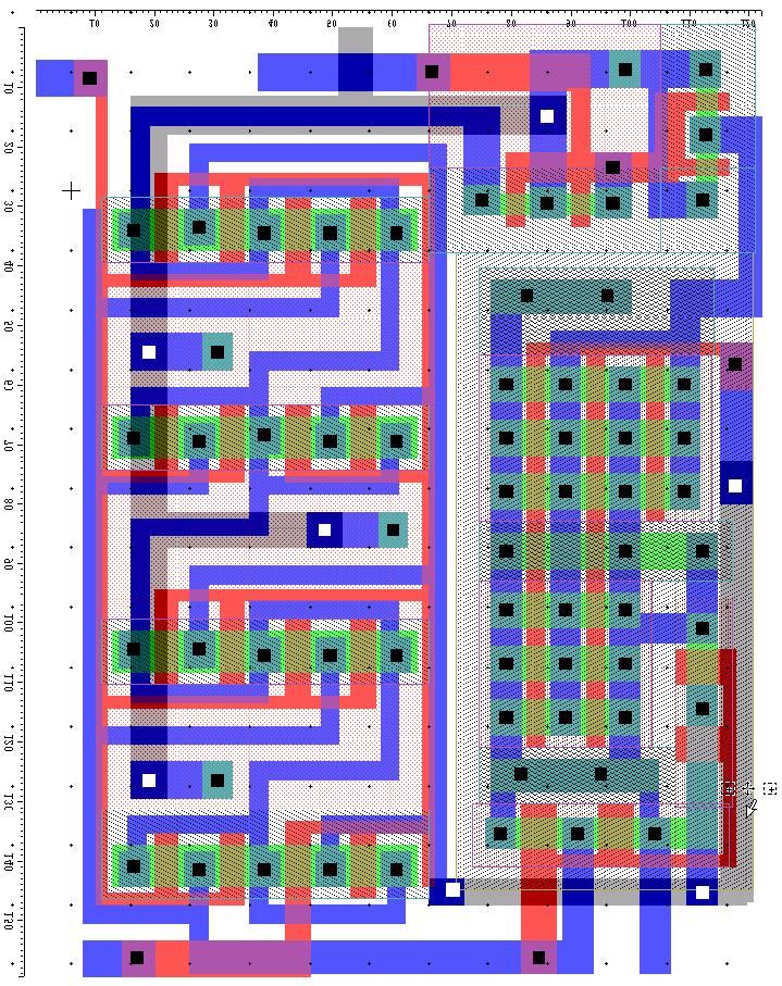
6 Layout Issues Prime considerations in the layout are those that are concerned with the matching of the two transistors and so as to be able to obtain minimum offset voltage, efficient placement of the body contact at a distance of every 50? and the minimization of the total size of the comparator. The transistors have to be laid out using design paradigms that calculate distances in units of? which measures 0.6µm in length. All transistor sizes are thus recalculated by dividing the actual sizes of the transistors by 0.6µ. Transistor sizes thus calculated are listed in Table V. Transistor Number Calculated Practical W L W L Table IV The magnitudes of the transistor sizes in terms of?. Both the theoretically calculated and the practical values used in the design are mentioned. Input Transistors The sizes of the input transistor sizes are large. It is necessary to divide the transistors into transistors of much smaller dimensions, and then connecting them up in parallel. In the present implementation, the transistors have been divided up into eight equal parts (so that each transistor was about 7? wide) and placed as shown in the Figure I below. The input transistors are matched using a method known as centroid matching. This effectively puts the two transistors evenly about a centroid position. The following diagram depicts this configuration schematically.
7 centroid Figure I A schematic representation of the method employed for centroid matching. Figure II depicts a schematic representation of the connection diagram. Fortunately, the two source terminals of the transistors are connected. This allows for a serpentine common source of the transistors. D2 Figure II A schematic representation of the connection diagram used for the layout. S1, S2 D1
8 Such a structure embodies the matching of the two transistors, is compact, and yet, uses only one metal for the interconnections. The problem of the above configuration lies in the amount of parasitic capacitance created due to the high amount of metal connections that have been used. Another problem that is not so evident is the intricate circuitry necessary for providing body contact within the structure. The layout of the schematic provides evidence of the greatest dexterity the designer has had to resort to, for providing body contacts effectively and efficiently. The Output Transistor The biggest of all the transistors is the output transistor M6 having a width of 88?. This has been divided up into 15 separate transistors and connected up in parallel. They are placed in an efficient manner so as to conserve space and consequently reduce the parasitic capacitances. Here again, the placement of the body contacts have been an extremely convoluted task. All other transistors have been small enough so as to obviate the need for intricate design. Nevertheless intelligent placement of the body contact has been necessary. The final layout area was 160µm x 130µm. Extraction of Parasitic Capacitances Parasitic capacitance extraction had been attempted. The spice file that resulted form the extraction process however did not contain any information of the values of the extracted capacitances. Internet searches to correctly extract the parasitic capacitances were in vain. The resultant spice parameter file however is appended at the end of the report for whatever it is worth. Results and Discussion The results of the synthesis have been briefly provided in Table V. These results have been further exemplified in the diagrams present in the annexure. Metrics Specifications (for 3mv p-p) Specifications (for 6mv p-p) Differential Voltage Gain Propagation Delay ns ns (rise edge) Propagation Delay ns ns (fall edge) Slew Rate (rise edge) V/µs V/µs Slew Rate(fall edge) V/µs V/µs Output Dynamic Range V (4.85V-4.946V) V (4.85V-4.946V)
9 Table V A brief summary of the results has been presented here. Measurements of slew rate, and propagation delay is done at an input differential voltage of 6mV peak-topeak. Differential Voltage Gain In the calculations, only the first stage gain was calculated and matched to 120V/V. The actual value of the first stage voltage gain (before the first stage was modified,) was given by 130V/V. The second stage thus had (and still has) a voltage gain of 10V/V. After modification of the first stage, the voltage gain of the first stage increased to 300V/V. The reason for the gain not doubling is that the length of and are not increased by a factor of 2 but increased from 1.6µm to 2µm. This allowed for the increase of the gain sufficiently so as to meet the specification, and yet, not increase the size of the transistors and especially since the W/L ratios of these transistors are great in the first place. Propagation Delay Calculations that have been done predicted that the circuit would have a propagation delay of less than 700ns. The propagation delay of the rising edge was significantly smaller than the propagation delay of the falling edge, and this is expected since the amount of current that can be provided by the larger transistor M6 is much greater than the current sinking capability of the much smaller transistor M7. Again the calculations pertain to the greater value, since the current equations that were used for finding the propagation delay depended upon the current carrying capability of the current mirroring transistor M7. The actual propagation delay ns corresponds closely to the calculated 700ns. Slew Rate Reasons identical to those of the above result in the slew rate of the rising edge to be much greater than the slew rate of the falling edge. The amplifier was designed to have a slew rate of something greater than 5 V/µs for reasons mentioned in the design procedure. The falling edge slew rate of V/µs corresponds to a not-tooclose approximation to the slew rate calculated and deemed necessary. Output Dynamic Range The output dynamic range limitation being most trivial has not been calculated. It is seen that the specifications for the output dynamic range has been more than met with. Common Mode Range The differential amplifiers have been designed so that none of the transistors go out of saturation for a common mode voltage of ±3.5V. A common mode voltage of ±3V have been applied to the transistor with a differential input voltage of 4mV. The comparator operated perfectly. Conclusion The comparator that has been designed meets all the specifications. It is intuitive to go through the utility of the comparator that has been designed. The comparator designed above would probably be used as an element of a generic ADC/DAC. Issues
10 that are of special interest for the proper and efficient functioning of the ADC/DAC are input offset voltage, slew rate, area considerations, and power consumption. Input Offset Voltage The input offset voltage of the comparator that has been designed is 4.04mV. This may be in excess of the input offset voltage that is inevitably created as a result of process irregularities and this additional input offset voltage may be additive. This has serious consequences. First this limits the resolution of the DAC. Second, if greater resolution is necessary, additional circuitry is necessary for minimizing the effect of this offset voltage, which would increases the size of the DAC. Slew Rate The slew rate of the comparator allows for a maximum bandwidth of about 354KHz [(3.54V/ µs)/ 10V]. In contemporary technology, DVD * video object sampling frequency is 48/96 KHz, and audio object sampling frequencies are 44.1/48/88.2/96/176.4/192 KHz, and CD quality music is recorded at 44.1KHz. Hence it is well suited for general audio/video ADC/DAC conversion. Area The area of the comparator is 160µm x 130µm such comparators would fill a 1cm x 1cm area of the chip. ADC/DACs made of such comparators shall take up much space. As the necessary precision requirement increases, one has to make even bigger comparators to nullify the effect of the slew rate. Power Consumption The power consumption of the comparator is of the order of 400µW. A 64-bit DAC built using this comparator would require W. Fifty such DAC/ACD should consume enough power to light up a flashlight! In summary, the designed comparator if used as part of an ADC would be useful in most generic audio/video applications. The word size of the comparator would be limited because of size and the power consumption related problems. Even though the parasitic capacitances have not been extracted, the slew rate is sufficiently high to make room for any feasible extra amount of capacitance and yet not compromise on the bandwidth to an extent that would render the device inoperable for generic audio/video applications. * Source: Source:
11
12 This document was created with Win2PDF available at The unregistered version of Win2PDF is for evaluation or non-commercial use only.
Design and Layout of Two Stage High Bandwidth Operational Amplifier
 Design and Layout of Two Stage High Bandwidth Operational Amplifier Yasir Mahmood Qureshi Abstract This paper presents the design and layout of a two stage, high speed operational amplifiers using standard
Radivoje Đurić, 2015, Analogna Integrisana Kola 1
 Low power OTA 1 Two-Stage, Miller Op Amp Operating in Weak Inversion Low frequency response: gm1 gm6 Av 0 g g g g A v 0 ds2 ds4 ds6 ds7 I D m, ds D nvt g g I n GB and SR: GB 1 1 n 1 2 4 6 6 7 g 2 2 m1
Design Analysis and Performance Comparison of Low Power High Gain 2nd Stage Differential Amplifier Along with 1st Stage
 Design Analysis and Performance Comparison of Low Power High Gain 2nd Stage Differential Amplifier Along with 1st Stage Sadeque Reza Khan Department of Electronic and Communication Engineering, National
Design and Simulation of Low Voltage Operational Amplifier
 Design and Simulation of Low Voltage Operational Amplifier Zach Nelson Department of Electrical Engineering, University of Nevada, Las Vegas 4505 S Maryland Pkwy, Las Vegas, NV 89154 United States of America
Advanced Operational Amplifiers
 IsLab Analog Integrated Circuit Design OPA2-47 Advanced Operational Amplifiers כ Kyungpook National University IsLab Analog Integrated Circuit Design OPA2-1 Advanced Current Mirrors and Opamps Two-stage
ECEN 474/704 Lab 6: Differential Pairs
 ECEN 474/704 Lab 6: Differential Pairs Objective Design, simulate and layout various differential pairs used in different types of differential amplifiers such as operational transconductance amplifiers
Radivoje Đurić, 2015, Analogna Integrisana Kola 1
 OTA-output buffer 1 According to the types of loads, the driving capability of the output stages differs. For switched capacitor circuits which have high impedance capacitive loads, class A output stage
IJSRD - International Journal for Scientific Research & Development Vol. 4, Issue 03, 2016 ISSN (online):
:") IJSRD - International Journal for Scientific Research & Development Vol. 4, Issue 03, 2016 ISSN (online): 2321-0613 Design and Analysis of Wide Swing Folded-Cascode OTA using 180nm Technology Priyanka
IJSRD - International Journal for Scientific Research & Development Vol. 4, Issue 03, 2016 ISSN (online): 2321-0613 Design and Analysis of Wide Swing Folded-Cascode OTA using 180nm Technology Priyanka
Lecture 300 Low Voltage Op Amps (3/28/10) Page 300-1
 Page 300-1") Lecture 300 Low Voltage Op Amps (3/28/10) Page 300-1 LECTURE 300 LOW VOLTAGE OP AMPS LECTURE ORGANIZATION Outline Introduction Low voltage input stages Low voltage gain stages Low voltage bias circuits
Lecture 300 Low Voltage Op Amps (3/28/10) Page 300-1 LECTURE 300 LOW VOLTAGE OP AMPS LECTURE ORGANIZATION Outline Introduction Low voltage input stages Low voltage gain stages Low voltage bias circuits
Design of a low voltage,low drop-out (LDO) voltage cmos regulator
 voltage cmos regulator") Design of a low,low drop-out (LDO) cmos regulator Chaithra T S Ashwini Abstract- In this paper a low, low drop-out (LDO) regulator design procedure is proposed and implemented using 0.25 micron CMOS process.
Design of a low,low drop-out (LDO) cmos regulator Chaithra T S Ashwini Abstract- In this paper a low, low drop-out (LDO) regulator design procedure is proposed and implemented using 0.25 micron CMOS process.
Low Quiescent Power CMOS Op-Amp in 0.5µm Technology
 Kevin Fronczak - Low Power CMOS Op-Amp - Rochester Institute of Technology EE610 1 Low Quiescent Power CMOS Op-Amp in 0.5µm Technology Kevin C. Fronczak Abstract This paper analyzes a low quiescent power
A Compact Folded-cascode Operational Amplifier with Class-AB Output Stage
 A Compact Folded-cascode Operational Amplifier with Class-AB Output Stage EEE 523 Advanced Analog Integrated Circuits Project Report Fuding Ge You are an engineer who is assigned the project to design
A 24 V Chopper Offset-Stabilized Operational Amplifier with Symmetrical RC Notch Filters having sub-10 µv offset and over-120db CMRR
 ROMANIAN JOURNAL OF INFORMATION SCIENCE AND TECHNOLOGY Volume 20, Number 4, 2017, 301 312 A 24 V Chopper Offset-Stabilized Operational Amplifier with Symmetrical RC Notch Filters having sub-10 µv offset
TWO AND ONE STAGES OTA
 TWO AND ONE STAGES OTA F. Maloberti Department of Electronics Integrated Microsystem Group University of Pavia, 7100 Pavia, Italy franco@ele.unipv.it tel. +39-38-50505; fax. +39-038-505677 474 EE Department
CMOS Operational Amplifier
 The George Washington University Department of Electrical and Computer Engineering Course: ECE218 Instructor: Mona E. Zaghloul Students: Shunping Wang Yiping (Neil) Tsai Data: 05/14/07 Introduction In
Design of a Folded Cascode Operational Amplifier in a 1.2 Micron Silicon-Carbide CMOS Process
 University of Arkansas, Fayetteville ScholarWorks@UARK Electrical Engineering Undergraduate Honors Theses Electrical Engineering 5-2017 Design of a Folded Cascode Operational Amplifier in a 1.2 Micron
A CMOS Low-Voltage, High-Gain Op-Amp
 A CMOS Low-Voltage, High-Gain Op-Amp G N Lu and G Sou LEAM, Université Pierre et Marie Curie Case 203, 4 place Jussieu, 75252 Paris Cedex 05, France Telephone: (33 1) 44 27 75 11 Fax: (33 1) 44 27 48 37
ISSN:
 468 Modeling and Design of a CMOS Low Drop-out (LDO) Voltage Regulator PRIYADARSHINI JAINAPUR 1, CHIRAG SHARMA 2 1 Department of E&CE, Nitte Meenakshi Institute of Technology, Yelahanka, Bangalore-560064,
Experiment #7 MOSFET Dynamic Circuits II
 Experiment #7 MOSFET Dynamic Circuits II Jonathan Roderick Introduction The previous experiment introduced the canonic cells for MOSFETs. The small signal model was presented and was used to discuss the
ALow Voltage Wide-Input-Range Bulk-Input CMOS OTA
 Analog Integrated Circuits and Signal Processing, 43, 127 136, 2005 c 2005 Springer Science + Business Media, Inc. Manufactured in The Netherlands. ALow Voltage Wide-Input-Range Bulk-Input CMOS OTA IVAN
ECEN 474/704 Lab 7: Operational Transconductance Amplifiers
 ECEN 474/704 Lab 7: Operational Transconductance Amplifiers Objective Design, simulate and layout an operational transconductance amplifier. Introduction The operational transconductance amplifier (OTA)
Chapter 5. Operational Amplifiers and Source Followers. 5.1 Operational Amplifier
 Chapter 5 Operational Amplifiers and Source Followers 5.1 Operational Amplifier In single ended operation the output is measured with respect to a fixed potential, usually ground, whereas in double-ended
ETIN25 Analogue IC Design. Laboratory Manual Lab 2
 Department of Electrical and Information Technology LTH ETIN25 Analogue IC Design Laboratory Manual Lab 2 Jonas Lindstrand Martin Liliebladh Markus Törmänen September 2011 Laboratory 2: Design and Simulation
Current Mirrors. Current Source and Sink, Small Signal and Large Signal Analysis of MOS. Knowledge of Various kinds of Current Mirrors
 Motivation Current Mirrors Current sources have many important applications in analog design. For example, some digital-to-analog converters employ an array of current sources to produce an analog output
Lecture 240 Cascode Op Amps (3/28/10) Page 240-1
 Page 240-1") Lecture 240 Cascode Op Amps (3/28/10) Page 2401 LECTURE 240 CASCODE OP AMPS LECTURE ORGANIZATION Outline Lecture Organization Single Stage Cascode Op Amps Two Stage Cascode Op Amps Summary CMOS Analog
Lecture 240 Cascode Op Amps (3/28/10) Page 2401 LECTURE 240 CASCODE OP AMPS LECTURE ORGANIZATION Outline Lecture Organization Single Stage Cascode Op Amps Two Stage Cascode Op Amps Summary CMOS Analog
Experiment 5 Single-Stage MOS Amplifiers
 Experiment 5 Single-Stage MOS Amplifiers B. Cagdaser, H. Chong, R. Lu, and R. T. Howe UC Berkeley EE 105 Fall 2005 1 Objective This is the first lab dealing with the use of transistors in amplifiers. We
Design and Simulation of Low Dropout Regulator
 Design and Simulation of Low Dropout Regulator Chaitra S Kumar 1, K Sujatha 2 1 MTech Student, Department of Electronics, BMSCE, Bangalore, India 2 Assistant Professor, Department of Electronics, BMSCE,
[Kumar, 2(9): September, 2013] ISSN: Impact Factor: 1.852
![[Kumar, 2(9): September, 2013] ISSN: Impact Factor: 1.852](/thumbs/86/94008668.jpg "[Kumar, 2(9): September, 2013] ISSN: Impact Factor: 1.852") IJESRT INTERNATIONAL JOURNAL OF ENGINEERING SCIENCES & RESEARCH TECHNOLOGY Design and Performance analysis of Low power CMOS Op-Amp Anand Kumar Singh *1, Anuradha 2, Dr. Vijay Nath 3 *1,2 Department of
IJESRT INTERNATIONAL JOURNAL OF ENGINEERING SCIENCES & RESEARCH TECHNOLOGY Design and Performance analysis of Low power CMOS Op-Amp Anand Kumar Singh *1, Anuradha 2, Dr. Vijay Nath 3 *1,2 Department of
NOVEMBER 29, 2017 COURSE PROJECT: CMOS TRANSIMPEDANCE AMPLIFIER ECG 720 ADVANCED ANALOG IC DESIGN ERIC MONAHAN
 NOVEMBER 29, 2017 COURSE PROJECT: CMOS TRANSIMPEDANCE AMPLIFIER ECG 720 ADVANCED ANALOG IC DESIGN ERIC MONAHAN 1.Introduction: CMOS Transimpedance Amplifier Avalanche photodiodes (APDs) are highly sensitive,
Rail to Rail Input Amplifier with constant G M and High Unity Gain Frequency. Arun Ramamurthy, Amit M. Jain, Anuj Gupta
 1 Rail to Rail Input Amplifier with constant G M and High Frequency Arun Ramamurthy, Amit M. Jain, Anuj Gupta Abstract A rail to rail input, 2.5V CMOS input amplifier is designed that amplifies uniformly
8. Combinational MOS Logic Circuits
 8. Combinational MOS Introduction Combinational logic circuits, or gates, witch perform Boolean operations on multiple input variables and determine the output as Boolean functions of the inputs, are the
COMPARISON OF THE MOSFET AND THE BJT:
 COMPARISON OF THE MOSFET AND THE BJT: In this section we present a comparison of the characteristics of the two major electronic devices: the MOSFET and the BJT. To facilitate this comparison, typical
G m /I D based Three stage Operational Amplifier Design
 G m /I D based Three stage Operational Amplifier Design Rishabh Shukla SVNIT, Surat shuklarishabh31081988@gmail.com Abstract A nested Gm-C compensated three stage Operational Amplifier is reviewed using
I1 19u 5V R11 1MEG IDC Q7 Q2N3904 Q2N3904. Figure 3.1 A scaled down 741 op amp used in this lab
 Lab 3: 74 Op amp Purpose: The purpose of this laboratory is to become familiar with a two stage operational amplifier (op amp). Students will analyze the circuit manually and compare the results with SPICE.
IOWA STATE UNIVERSITY. EE501 Project. Fully Differential Multi-Stage Op-Amp Design. Ryan Boesch 11/12/2008
 IOWA STATE UNIVERSITY EE501 Project Fully Differential Multi-Stage Op-Amp Design Ryan Boesch 11/12/2008 This report documents the design, simulation, layout, and post-layout simulation of a fully differential
DAT175: Topics in Electronic System Design
 DAT175: Topics in Electronic System Design Analog Readout Circuitry for Hearing Aid in STM90nm 21 February 2010 Remzi Yagiz Mungan v1.10 1. Introduction In this project, the aim is to design an adjustable
AN Analog Power USA Applications Department
 Using MOSFETs for Synchronous Rectification The use of MOSFETs to replace diodes to reduce the voltage drop and hence increase efficiency in DC DC conversion circuits is a concept that is widely used due
Analog Integrated Circuit Design Exercise 1
 Analog Integrated Circuit Design Exercise 1 Integrated Electronic Systems Lab Prof. Dr.-Ing. Klaus Hofmann M.Sc. Katrin Hirmer, M.Sc. Sreekesh Lakshminarayanan Status: 21.10.2015 Pre-Assignments The lecture
DESIGN HIGH SPEED, LOW NOISE, LOW POWER TWO STAGE CMOS OPERATIONAL AMPLIFIER. Himanshu Shekhar* 1, Amit Rajput 1
 ISSN 2277-2685 IJESR/June 2014/ Vol-4/Issue-6/319-323 Himanshu Shekhar et al./ International Journal of Engineering & Science Research DESIGN HIGH SPEED, LOW NOISE, LOW POWER TWO STAGE CMOS OPERATIONAL
LOW VOLTAGE ANALOG IC DESIGN PROJECT 1. CONSTANT Gm RAIL TO RAIL INPUT STAGE DESIGN. Prof. Dr. Ali ZEKĐ. Umut YILMAZER
 LOW VOLTAGE ANALOG IC DESIGN PROJECT 1 CONSTANT Gm RAIL TO RAIL INPUT STAGE DESIGN Prof. Dr. Ali ZEKĐ Umut YILMAZER 1 1. Introduction In this project, two constant Gm input stages are designed. First circuit
A 16Ω Audio Amplifier with 93.8 mw Peak loadpower and 1.43 quiscent power consumption
 A 16Ω Audio Amplifier with 93.8 mw Peak loadpower and 1.43 quiscent power consumption IEEE Transactions on circuits and systems- Vol 59 No:3 March 2012 Abstract A class AB audio amplifier is used to drive
Experiment #6 MOSFET Dynamic circuits
 Experiment #6 MOSFET Dynamic circuits Jonathan Roderick Introduction: This experiment will build upon the concepts that were presented in the previous lab and introduce dynamic circuits using MOSFETS.
Design of High Gain Low Voltage CMOS Comparator
 Design of High Gain Low Voltage CMOS Comparator Shahid Khan 1 1 Rustomjee Academy for Global Careers Abstract: Comparators used in most of the analog circuits like analog to digital converters, switching
A PSEUDO-CLASS-AB TELESCOPIC-CASCODE OPERATIONAL AMPLIFIER
 A PSEUDO-CLASS-AB TELESCOPIC-CASCODE OPERATIONAL AMPLIFIER M. Taherzadeh-Sani, R. Lotfi, and O. Shoaei ABSTRACT A novel class-ab architecture for single-stage operational amplifiers is presented. The structure
0.85V. 2. vs. I W / L
 EE501 Lab3 Exploring Transistor Characteristics and Design Common-Source Amplifiers Lab report due on September 22, 2016 Objectives: 1. Be familiar with characteristics of MOSFET such as gain, speed, power,
Obsolete Product(s) - Obsolete Product(s)
 - Obsolete Product(s)") Low power quad operational amplifier Features Wide gain bandwidth: 1.3 MHz Extended temperature range: -40 C to +150 C Input common-mode voltage range includes negative rail Large voltage gain: 100 db
Low power quad operational amplifier Features Wide gain bandwidth: 1.3 MHz Extended temperature range: -40 C to +150 C Input common-mode voltage range includes negative rail Large voltage gain: 100 db
Lecture 330 Low Power Op Amps (3/27/02) Page 330-1
 Page 330-1") Lecture 33 Low Power Op Amps (3/27/2) Page 33 LECTURE 33 LOW POWER OP AMPS (READING: AH 39342) Objective The objective of this presentation is:.) Examine op amps that have minimum static power Minimize
Lecture 33 Low Power Op Amps (3/27/2) Page 33 LECTURE 33 LOW POWER OP AMPS (READING: AH 39342) Objective The objective of this presentation is:.) Examine op amps that have minimum static power Minimize
60V High-Speed Precision Current-Sense Amplifier
 EVALUATION KIT AVAILABLE MAX9643 General Description The MAX9643 is a high-speed 6V precision unidirectional current-sense amplifier ideal for a wide variety of power-supply control applications. Its high
Topology Selection: Input
 Project #2: Design of an Operational Amplifier By: Adrian Ildefonso Nedeljko Karaulac I have neither given nor received any unauthorized assistance on this project. Process: Baker s 50nm CAD Tool: Cadence
James Lunsford HW2 2/7/2017 ECEN 607
 James Lunsford HW2 2/7/2017 ECEN 607 Problem 1 Part A Figure 1: Negative Impedance Converter To find the input impedance of the above NIC, we use the following equations: V + Z N V O Z N = I in, V O kr
LECTURE 19 DIFFERENTIAL AMPLIFIER
 Lecture 19 Differential Amplifier (6/4/14) Page 191 LECTURE 19 DIFFERENTIAL AMPLIFIER LECTURE ORGANIZATION Outline Characterization of a differential amplifier Differential amplifier with a current mirror
UMAINE ECE Morse Code ROM and Transmitter at ISM Band Frequency
 UMAINE ECE Morse Code ROM and Transmitter at ISM Band Frequency Jamie E. Reinhold December 15, 2011 Abstract The design, simulation and layout of a UMAINE ECE Morse code Read Only Memory and transmitter
High Voltage and Temperature Auto Zero Op-Amp Cell Features Applications Process Technology Introduction Parameter Unit Rating
 Analogue Integration AISC11 High Voltage and Temperature Auto Zero Op-Amp Cell Rev.1 12-1-5 Features High Voltage Operation: 4.5-3 V Precision, Auto-Zeroed Input Vos High Temperature Operation Low Quiescent
Design of Analog and Mixed Integrated Circuits and Systems Theory Exercises
 102726 Design of nalog and Mixed Theory Exercises Francesc Serra Graells http://www.cnm.es/~pserra/uab/damics paco.serra@imb-cnm.csic.es 1 Introduction to the Design of nalog Integrated Circuits 1.1 The
A new class AB folded-cascode operational amplifier
 A new class AB folded-cascode operational amplifier Mohammad Yavari a) Integrated Circuits Design Laboratory, Department of Electrical Engineering, Amirkabir University of Technology, Tehran, Iran a) myavari@aut.ac.ir
Micropower, Single-Supply, Rail-to-Rail, Precision Instrumentation Amplifiers MAX4194 MAX4197
 General Description The is a variable-gain precision instrumentation amplifier that combines Rail-to-Rail single-supply operation, outstanding precision specifications, and a high gain bandwidth. This
Linear IC s and applications
 Questions and Solutions PART-A Unit-1 INTRODUCTION TO OP-AMPS 1. Explain data acquisition system Jan13 DATA ACQUISITION SYSYTEM BLOCK DIAGRAM: Input stage Intermediate stage Level shifting stage Output
Lecture 11 Digital Circuits (I) THE INVERTER
 THE INVERTER") Lecture 11 Digital Circuits (I) THE INVERTER Outline Introduction to digital circuits The inverter NMOS inverter with resistor pull-up Reading Assignment: Howe and Sodini; Chapter 5, Sections 5.1-5.3 6.12
Lecture 11 Digital Circuits (I) THE INVERTER Outline Introduction to digital circuits The inverter NMOS inverter with resistor pull-up Reading Assignment: Howe and Sodini; Chapter 5, Sections 5.1-5.3 6.12
Dual operational amplifier
 DESCRIPTION The 77 is a pair of high-performance monolithic operational amplifiers constructed on a single silicon chip. High common-mode voltage range and absence of latch-up make the 77 ideal for use
Electronics Prof. D. C. Dube Department of Physics Indian Institute of Technology, Delhi
 Electronics Prof. D. C. Dube Department of Physics Indian Institute of Technology, Delhi Module No # 05 FETS and MOSFETS Lecture No # 06 FET/MOSFET Amplifiers and their Analysis In the previous lecture
Design of an Amplifier for Sensor Interfaces
 Design of an Amplifier for Sensor Interfaces Anurag Mangla Electrical and Electronics Engineering anurag.mangla@epfl.ch Supervised by Dr. Marc Pastre Prof. Maher Kayal Outline Introduction Need for high
Laboratory 8 Operational Amplifiers and Analog Computers
 Laboratory 8 Operational Amplifiers and Analog Computers Introduction Laboratory 8 page 1 of 6 Parts List LM324 dual op amp Various resistors and caps Pushbutton switch (SPST, NO) In this lab, you will
Low Power Op-Amp Based on Weak Inversion with Miller-Cascoded Frequency Compensation
 Low Power Op-Amp Based on Weak Inversion with Miller-Cascoded Frequency Compensation Maryam Borhani, Farhad Razaghian Abstract A design for a rail-to-rail input and output operational amplifier is introduced.
CMOS RE-CONFIGURABLE MULTI-STANDARD RADIO RECEIVERS BIASING ANALYSIS
 Électronique et transmission de l information CMOS RE-CONFIGURABLE MULTI-STANDARD RADIO RECEIVERS BIASING ANALYSIS SILVIAN SPIRIDON, FLORENTINA SPIRIDON, CLAUDIUS DAN, MIRCEA BODEA Key words: Software
Low Cost, General Purpose High Speed JFET Amplifier AD825
 a FEATURES High Speed 41 MHz, 3 db Bandwidth 125 V/ s Slew Rate 8 ns Settling Time Input Bias Current of 2 pa and Noise Current of 1 fa/ Hz Input Voltage Noise of 12 nv/ Hz Fully Specified Power Supplies:
Designing a 960 MHz CMOS LNA and Mixer using ADS. EE 5390 RFIC Design Michelle Montoya Alfredo Perez. April 15, 2004
 Designing a 960 MHz CMOS LNA and Mixer using ADS EE 5390 RFIC Design Michelle Montoya Alfredo Perez April 15, 2004 The University of Texas at El Paso Dr Tim S. Yao ABSTRACT Two circuits satisfying the
DIGITALLY controlled and area-efficient calibration circuits
 246 IEEE TRANSACTIONS ON CIRCUITS AND SYSTEMS II: EXPRESS BRIEFS, VOL. 52, NO. 5, MAY 2005 A Low-Voltage 10-Bit CMOS DAC in 0.01-mm 2 Die Area Brandon Greenley, Raymond Veith, Dong-Young Chang, and Un-Ku
Class-AB Low-Voltage CMOS Unity-Gain Buffers
 Class-AB Low-Voltage CMOS Unity-Gain Buffers Mariano Jimenez, Antonio Torralba, Ramón G. Carvajal and J. Ramírez-Angulo Abstract Class-AB circuits, which are able to deal with currents several orders of
NE/SA/SE532 LM258/358/A/2904 Low power dual operational amplifiers
 INTEGRATED CIRCUITS NE/SA/SE53 Supersedes data of Jan Jul 1 DESCRIPTION The 53/358/LM94 consists of two independent, high gain, internally frequency-compensated operational amplifiers internally frequency-compensated
Current Source/Sinks
 Motivation Current Source/Sinks Biasing is a very important step in MOS based analog design. A current sink and current source are two terminal components whose current at any instant of time is independent
Common Mode Feedback for Fully Differential Amplifier in ami06 micron CMOS process
 Published by : http:// Common Mode Feedback for Fully Differential Amplifier in ami06 micron CMOS process Ravi Teja Bojanapally Department of Electrical and Computer Engineering, Texas Tech University,
A 2.4 GHZ RECEIVER IN SILICON-ON-SAPPHIRE MICHAEL PETERS. B.S., Kansas State University, 2009 A REPORT
 A 2.4 GHZ RECEIVER IN SILICON-ON-SAPPHIRE by MICHAEL PETERS B.S., Kansas State University, 2009 A REPORT submitted in partial fulfillment of the requirements for the degree MASTER OF SCIENCE Department
Design of High-Speed Op-Amps for Signal Processing
 Design of High-Speed Op-Amps for Signal Processing R. Jacob (Jake) Baker, PhD, PE Professor and Chair Boise State University 1910 University Dr. Boise, ID 83725-2075 jbaker@ieee.org Abstract - As CMOS
Low Power and Fast Transient High Swing CMOS Telescopic Operational Amplifier
 RESEARCH ARTICLE OPEN ACCESS Low Power and Fast Transient High Swing CMOS Telescopic Operational Amplifier Akshay Kumar Kansal 1, Asst Prof. Gayatri Sakya 2 Electronics and Communication Department, 1,2
Non-linear Control. Part III. Chapter 8
 Chapter 8 237 Part III Chapter 8 Non-linear Control The control methods investigated so far have all been based on linear feedback control. Recently, non-linear control techniques related to One Cycle
You will be asked to make the following statement and provide your signature on the top of your solutions.
 1 EE 435 Name Exam 1 Spring 2018 Instructions: The points allocated to each problem are as indicated. Note that the first and last problem are weighted more heavily than the rest of the problems. On those
A Novel Design of Low Voltage,Wilson Current Mirror based Wideband Operational Transconductance Amplifier
 A Novel Design of Low Voltage,Wilson Current Mirror based Wideband Operational Transconductance Amplifier Kehul A. Shah 1, N.M.Devashrayee 2 1(Associative Prof., Department of Electronics and Communication,
PAD: Procedural Analog Design Tool D. Stefanovic, M. Kayal, M. Pastre
 PAD: Procedural Analog Design Tool D. Stefanovic, M. Kayal, M. Pastre Swiss Federal Institute of Technology, Electronic Labs, STI/IMM/LEG, Lausanne, Switzerland Procedural Analog Design Tool Interactive
Lecture 11 Circuits numériques (I) L'inverseur
 L'inverseur") Lecture 11 Circuits numériques (I) L'inverseur Outline Introduction to digital circuits The inverter NMOS inverter with resistor pull-up 6.12 Spring 24 Lecture 11 1 1. Introduction to digital circuits:
Lecture 11 Circuits numériques (I) L'inverseur Outline Introduction to digital circuits The inverter NMOS inverter with resistor pull-up 6.12 Spring 24 Lecture 11 1 1. Introduction to digital circuits:
Design of Gain Enhanced and Power Efficient Op- Amp for ADC/DAC and Medical Applications
 Indian Journal of Science and Technology, Vol 9(29), DOI: 10.17485/ijst/2016/v9i29/90885, August 2016 ISSN (Print) : 0974-6846 ISSN (Online) : 0974-5645 Design of Gain Enhanced and Power Efficient Op-
Low-Power, Precision, 4-Bump WLP, Current-Sense Amplifier
 EVALUATION KIT AVAILABLE General Description The is a zero-drift, high-side current-sense amplifier family that offers precision, low supply current and is available in a tiny 4-bump ultra-thin WLP of
Chapter 2 CMOS at Millimeter Wave Frequencies
 Chapter 2 CMOS at Millimeter Wave Frequencies In the past, mm-wave integrated circuits were always designed in high-performance RF technologies due to the limited performance of the standard CMOS transistors
LP2902/LP324 Micropower Quad Operational Amplifier
 LP2902/LP324 Micropower Quad Operational Amplifier General Description The LP324 series consists of four independent, high gain internally compensated micropower operational amplifiers. These amplifiers
AVoltage Controlled Oscillator (VCO) was designed and
 was designed and") 1 EECE 457 VCO Design Project Jason Khuu, Erik Wu Abstract This paper details the design and simulation of a Voltage Controlled Oscillator using a 0.13µm process. The final VCO design meets all specifications.
1 EECE 457 VCO Design Project Jason Khuu, Erik Wu Abstract This paper details the design and simulation of a Voltage Controlled Oscillator using a 0.13µm process. The final VCO design meets all specifications.
SOLIMAN A. MAHMOUD Department of Electrical Engineering, Faculty of Engineering, Cairo University, Fayoum, Egypt
 Journal of Circuits, Systems, and Computers Vol. 14, No. 4 (2005) 667 684 c World Scientific Publishing Company DIGITALLY CONTROLLED CMOS BALANCED OUTPUT TRANSCONDUCTOR AND APPLICATION TO VARIABLE GAIN
Chapter 12 Opertational Amplifier Circuits
 1 Chapter 12 Opertational Amplifier Circuits Learning Objectives 1) The design and analysis of the two basic CMOS op-amp architectures: the two-stage circuit and the single-stage, folded cascode circuit.
A New Design Technique of CMOS Current Feed Back Operational Amplifier (CFOA)
") Circuits and Systems, 2013, 4, 11-15 http://dx.doi.org/10.4236/cs.2013.41003 Published Online January 2013 (http://www.scirp.org/journal/cs) A New Design Technique of CMOS Current Feed Back Operational
Circuits and Systems, 2013, 4, 11-15 http://dx.doi.org/10.4236/cs.2013.41003 Published Online January 2013 (http://www.scirp.org/journal/cs) A New Design Technique of CMOS Current Feed Back Operational
IN RECENT years, low-dropout linear regulators (LDOs) are
 are") IEEE TRANSACTIONS ON CIRCUITS AND SYSTEMS II: EXPRESS BRIEFS, VOL. 52, NO. 9, SEPTEMBER 2005 563 Design of Low-Power Analog Drivers Based on Slew-Rate Enhancement Circuits for CMOS Low-Dropout Regulators
IEEE TRANSACTIONS ON CIRCUITS AND SYSTEMS II: EXPRESS BRIEFS, VOL. 52, NO. 9, SEPTEMBER 2005 563 Design of Low-Power Analog Drivers Based on Slew-Rate Enhancement Circuits for CMOS Low-Dropout Regulators
INF3410 Fall Book Chapter 6: Basic Opamp Design and Compensation
 INF3410 Fall 2013 Compensation content Introduction Two Stage Opamps Compensation Slew Rate Systematic Offset Advanced Current Mirrors Operational Transconductance Amplifiers Current Mirror Opamps Folded
8-Bit, high-speed, µp-compatible A/D converter with track/hold function ADC0820
 8-Bit, high-speed, µp-compatible A/D converter with DESCRIPTION By using a half-flash conversion technique, the 8-bit CMOS A/D offers a 1.5µs conversion time while dissipating a maximum 75mW of power.
LM2904AH. Low-power, dual operational amplifier. Related products. Description. Features. See LM2904WH for enhanced ESD performances
 LM2904AH Low-power, dual operational amplifier Datasheet - production data Related products See LM2904WH for enhanced ESD performances Features Frequency compensation implemented internally Large DC voltage
A high-speed CMOS current op amp for very low supply voltage operation
 Downloaded from orbit.dtu.dk on: Mar 31, 2018 A high-speed CMOS current op amp for very low supply voltage operation Bruun, Erik Published in: Proceedings of the IEEE International Symposium on Circuits
Analysis and Design of High Speed Low Power Comparator in ADC
 Analysis and Design of High Speed Low Power Comparator in ADC 1 Abhishek Rai, 2 B Ananda Venkatesan 1 M.Tech Scholar, 2 Assistant professor Dept. of ECE, SRM University, Chennai 1 Abhishekfan1791@gmail.com,
ISSCC 2004 / SESSION 26 / OPTICAL AND FAST I/O / 26.8
 ISSCC 2004 / SESSION 26 / OPTICAL AND FAST I/O / 26.8 26.8 A 2GHz CMOS Variable-Gain Amplifier with 50dB Linear-in-Magnitude Controlled Gain Range for 10GBase-LX4 Ethernet Chia-Hsin Wu, Chang-Shun Liu,
Rail to rail CMOS complementary input stage with only one active differential pair at a time
 LETTER IEICE Electronics Express, Vol.11, No.12, 1 5 Rail to rail CMOS complementary input stage with only one active differential pair at a time Maria Rodanas Valero 1a), Alejandro Roman-Loera 2, Jaime
A Novel Continuous-Time Common-Mode Feedback for Low-Voltage Switched-OPAMP
 10.4 A Novel Continuous-Time Common-Mode Feedback for Low-oltage Switched-OPAMP M. Ali-Bakhshian Electrical Engineering Dept. Sharif University of Tech. Azadi Ave., Tehran, IRAN alibakhshian@ee.sharif.edu
SGM ns, Low-Power, 3V/5V, Rail-to-Rail Input Single-Supply Comparator
 45ns, Low-Power, 3V/5V, Rail-to-Rail GENERAL DESCRIPTION The is a single high-speed comparator optimized for systems powered from a 3V or 5V supply. The device features high-speed response, low-power consumption,
MP5120, MP5220, MP5420 High Speed, +/-9V, Rail-to-Rail Input-Output Op Amps
 The Future of Analog IC Technology MP2, MP22, MP2 High Speed, /-9V, Rail-to-Rail Input-Output Op Amps DESCRIPTION The MP2 (single), MP22 (dual), and MP2 (quad) are high-speed, high-voltage rail-to-rail
MICROELECTRONIC CIRCUIT DESIGN Third Edition
 MICROELECTRONIC CIRCUIT DESIGN Third Edition Richard C. Jaeger and Travis N. Blalock Answers to Selected Problems Updated 1/25/08 Chapter 1 1.3 1.52 years, 5.06 years 1.5 1.95 years, 6.46 years 1.8 113
A Switched-Capacitor Band-Pass Biquad Filter Using a Simple Quasi-unity Gain Amplifier
 A Switched-Capacitor Band-Pass Biquad Filter Using a Simple Quasi-unity Gain Amplifier Hugo Serra, Nuno Paulino, and João Goes Centre for Technologies and Systems (CTS) UNINOVA Dept. of Electrical Engineering