Hetero Silicon Photonics: Components, systems, packaging and beyond
|
|
|
- Aileen Parks
- 5 years ago
- Views:
Transcription
1 Silicon Photonics Hetero Silicon Photonics: Components, systems, packaging and beyond Thursday, October 9, 2014 Tolga Tekin and Rifat Kisacik Photonic & Plasmonic Systems, Fraunhofer for Reliability and Microintegration (IZM)

2 Moore s Law and More Technological frontiers between semiconductor technology, packaging, and system design are tending to disappear. Designers of chips, packages, and systems will have to work closer together than ever before in order to drive the performance for future microelectronic systems. Gordon Moore The semiconductor technology is heading the basic physical limits to CMOS scaling. The scaling geometries alone do not ensure improvement of performance, less power, smaller size, and lower cost. It will require More than Moore through the tighter integration of system level components at the package level. (ITRS) 2
3 Bottleneck A key bottleneck to the realization of high-performance microelectronic systems, including SiP, is the lack of low-latency, high-bandwidth, and high density off-chip interconnects. Some of the challenges in achieving high-bandwidth chip-to-chip communication using electrical interconnects include the high losses in the substrate dielectric, reflections and impedance discontinuities, and susceptibility to crosstalk. Obviously, the motivation for the use of photonics to overcome these challenges and leverage low-latency and high-bandwidth communication. The objective is to develop a CMOS compatible underlying technology to enable next generation photonic layer within the 3D SiP towards converged microsystems Tekin, T.;, "Review of Packaging of Optoelectronic, Photonic, and MEMS Components," Selected Topics in Quantum Electronics, IEEE Journal of, vol.17, no.3, pp , May-June 2011 doi: /JSTQE
4 Converging Technologies Converging technologies are shaping the future of our society. Boarders between disciplines are disappearing. Information and communication technology transformed our daily life in last century. New technologies such as nanotechnology have significant potential for further transformation. ICT manufacturing concepts, instead of very specialized production lines more and more generic approaches are required to serve a broader area of interest Concentrated know-how and the enormous qualified technology base is available from some institutional core-players in the research field of packaging. 4


5 The Enabling Technology? Electronics Electrical interconnects: limited by RC-delay Electronics is aspect-ratio limited in speed..but still the most mature intelligence platform 5

 Si Source: IBM SiO 2 Light")
6 The Enabling Technology? Silicon Photonics Source: AMO Integrated optical components based on Silicon Energy-efficient, high bandwidth data communication on short distances Bit rate is limited only by the carrier frequency (100Tb/s) Si Source: IBM SiO 2 Light propagation: subjected to diffraction down-limits component size 6


7 The Enabling Technology? Plasmonics Propagation of Surface Plasmon Polariton (SPP) modes using metallic nanostructures EM waves guided at the metal/dielectric interface Sub-wavelength confinement! No limitations in speed and size 7 Seamless interface between optics-electronics Loss
8 Operating speed Combine Benefits On-Chip 1THz 1GHz 1MHz 1kHz Diffraction limit Plasmonics Photonics Electronics The Past RC-delay limit The next chip-scale technology!!! R. Zia et al., Plasmonics: the next chip-scale technology, Materials Today 9(7-8), 2006 D. K. Gramotnev and S. I. Bozhevolnyi, Plasmonics beyond the diffraction limit, Nature Nanophotonics 4(2), nm 100nm 1μm 10μm 100μm 1mm Critical dimension electronics for smart functions (processing, control) Silicon photonics for low-loss passive optics Plasmonics for low-power active functions 8

 Guide Light")


 Low Cost Assembly 6)")

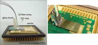
9 Quo vadis? Merging of Silicon Electronics and Photonics 1) Light Source 2) Guide Light 3) Fast Modulation External Cavity Laser Light Source Waveguides Tapers Silicon Modulator Splitters Switches, Couplers, & others 4) Detect Light 5) Low Cost Assembly 6) Intelligence Passive Alignment CMOS Photo-Detector BUILDING BLOCKS OF SILICON PHOTONICS by Intel 9


10 Silicon Photonics Activities at Fraunhofer IZM epixnet HELIOS PLATON iphos RAMPLAS PARADIGM UPVLC PhoxTroT COMANDER 10
11 Fraunhofer IZM s Concept 11
12 Quo vadis? Merging of Silicon Electronics and Photonics 1) Light Source 2) Guide Light 3) Fast Modulation External Cavity Laser Light Source Waveguides Tapers Silicon Modulator Splitters Switches, Couplers, & others 4) Detect Light 5) Low Cost Assembly 6) Intelligence Passive Alignment CMOS Photo-Detector BUILDING BLOCKS OF SILICON PHOTONICS by Intel 12

13 In the Age of Converging Technologies FACT: System complexity and functionality are increasing TARGET: Seamless applications (ICT) FIRST STEP: Generic foundry and packaging approaches That can be satisfied by heterogeneous integration of different technologies, leading to the best compromise in systems functionality and cost of ownership for higher multi functional converging systems. All these technologies need to be optimized All these technologies need to be adapted into a modular integrated process flow. 13


14 Hetero Silicon Photonics - Integration Platform Targeting high-performance, low-cost, low-energy and small-size components across the entire interconnect hierarchy level can definitely not rely on a single technology platform. VSI OBJECTIVE Create the optimal synergies between different technologies streamlining their deployment towards Tb/sscale, high-performance, low-cost and low-energy optical interconnect components and sub-systems Mix & Match components / building blocks to deliver the optimal heterogeneous integration and to align their synergistic deployment towards the specific needs of individual functions Tolga Tekin, Michael Töpper and Herbert Reichl, "PICSiP: new system-in-package technology using a high bandwidth photonic interconnection layer for converged microsystems", Proc. SPIE 7366, (2009); 14
 and")
15 Silicon Interposer with Optical Layer adaptation to 3D VSI process flow oe chip metallization isolation Si BOX Cu TSV isolation 3D wafer-level system integration (300mm wafer) Silicon interposer technology with high-density Die-to-wafer and wafer-to-wafer bonding wiring Wafer-level assembly and 3D stacking Interposers with high-density Cu-TSV Evaluation of die-to-wafer (D2W) and wafer-to-carriewafer (W2W) assembly technologies High-density multilayer copper wiring (min. 2μm line /space) 3D IC assembly with high-density interconnects Embedding of active and passive devices into the (> 1000 I/O) and ultra-fine pitch (< 50μm) silicon interposer 3D IC assembly with thin and ultra-thin chips (20- Wafer thinning and handling technology 150μm) device wafer thickness: <20 μm Through silicon via technology Temporary wafer bonding and debonding TSV diameter: 2 20μm; technology aspect ratio: 5 to 30 Wafer bumping technology 15 back side isolation Leveraging know-how, experience and technology of 3D heterogeneous integration, including system-in-package


 Transmission")
16 Building-Blocks for Hetero Silicon Photonics Optical Optical waveguides Coupling to fiber 3dB splitter Ring resonators MUX/DEMUX Switches MZI Electro-optical Photodetectors Light sources: LED, VCSEL Electrical Through-Silicon Vias (TSV) Transmission line: CPW, slotline Antenna Heater developed in following projects 16

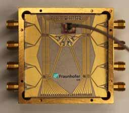
17 PLATON - Merging Plasmonics and Silicon Photonics Technology Towards Tb/s Routing in Optical Interconnects Fiber to Si coupler MUX Waveguides Photodiode Si to DLSPP coupler Electrical wiring Locig IC Hetero Silicon Photonics platform Tolga Tekin, Alpaslan Suna, Oriol Gili de Villasante, Paul Tcheg, Bei Wang, Sascha Lutzmann, Bouchaib Bouhlal, Nikos Pleros, Emmanouil Kriezis, Matthias Baus and Matthias Karl, "Photonic integrated system-in-package platform for Tb/s silicon-plasmonic router", Proc. SPIE 8265, 82650B (2012); 17


18 RAMPLAS Gb/s Optical RAM On-Chip: Silicon-Based, Integrated Optical RAM 100GHz Bit Processing: Exploit novel InGaAsP-NSb dilute nitride/antimonide compounds SOA for 1ps response time 64-bit optical RAM bank: Hetero Silicon Photonic integration: Silicon nanowires and GaAs-on-SOI technology for dense/large scale integration Novel Architectures: WDM towards dynamic optical cache mapping Reduce losses for multiple inputs & output chip to chip optical 18
 http://www.iphos-project.")
19 IPHOS - Integrated photonic transceivers at sub-terahertz wave range for ultra-wideband wireless communications Optical techniques to generate the carrier wave, enabling us to integrate a high level of functionality (carrier wave tunability, data modulation) Hetero Silicon based integration platform V-groove for the precise alignment of fiber Location of PD, LNA and PA; possibly close to each Biasing networks for PD and amplifiers to minimize RF signal transmission CPW to WR12 waveguide transition with low return loss B. Bouhlal, S. Lutzmann, M. Palandöken, V. Rymanov, A. Stöhr, T. Tekin Integration platform for 72 GHz photodiode-based wireless transmitter Proceedings of SPIE Volume 8259, 2012.; 19
20 Heterogeneous Integration Silicon Photonics as integration platform Designed by IZM Fabricated in AMO Chracterized in IZM Integrated in IZM Plasmonics switches Designed by SDU Fabricated in UB Chracterized in IZM Integrated in IZM Control IC Designed by IZM Fabricated in ams Chracterized in IZM Integrated in IZM Fiber to Si coupler MUX Waveguides Electrical wiring Si to DLSPP interface Plasmonic switching elements Logic IC PLATON SOI Platform 20
21 Advanced packaging technologies will improve future systems: 1. Packaging determines functionality, cost and reliability of future systems. 2. System-in-Package is the way for future subsystems. 3. Future systems are very high complex systems and contain different physical functions. Therefore modularity in heterogeneous integration is required. 4. Future systems combine optical and ultra high frequency functions. They contain antennas, batteries, sensors, optical components, and microelectronic devices. With this a large variety of materials will be applied. For all these components a common smart support substrate such as Silicon will be of importance for future systems. HETERO SILICON PHOTONICS - Integration Platform Tekin, T.;, "Review of Packaging of Optoelectronic, Photonic, and MEMS Components," Selected Topics in Quantum Electronics, IEEE Journal of, vol.17, no.3, pp , May-June 2011 doi: /JSTQE


22 PhoxTroT PhoxTroT is a large-scale European research effort focusing on high-performance, low-energy, low-cost, small-size Optical interconnects across the whole data center ecosystem: on-board, board-to-board and rack-to-rack. 22

23 Hetero Silicon Photonics increasing optical functionalities 23
Fraunhofer IZM - ASSID
 FRAUNHOFER-INSTITUT FÜR Zuverlässigkeit und Mikrointegration IZM Fraunhofer IZM - ASSID All Silicon System Integration Dresden Heterogeneous 3D Wafer Level System Integration 3D system integration is one
D6.3: Evaluation of the 2nd generation 2x2 PLATON optical interconnect router
 ICT - Information and Communication Technologies Merging Plasmonics and Silicon Photonics Technology towards Tb/s routing in optical interconnects Collaborative Project Grant Agreement Number 249135 D6.3:
IEEE JOURNAL OF SELECTED TOPICS IN QUANTUM ELECTRONICS 2010 Silicon Photonic Circuits: On-CMOS Integration, Fiber Optical Coupling, and Packaging
 IEEE JOURNAL OF SELECTED TOPICS IN QUANTUM ELECTRONICS 2010 Silicon Photonic Circuits: On-CMOS Integration, Fiber Optical Coupling, and Packaging Christophe Kopp, St ephane Bernab e, Badhise Ben Bakir,
Lecture: Integration of silicon photonics with electronics. Prepared by Jean-Marc FEDELI CEA-LETI
 Lecture: Integration of silicon photonics with electronics Prepared by Jean-Marc FEDELI CEA-LETI Context The goal is to give optical functionalities to electronics integrated circuit (EIC) The objectives
Overview and Roadmap for European projects in Optical Interconnects
 Overview and Roadmap for European projects in Optical Interconnects Dptm. of Informatics, Aristotle Univ. of Thessaloniki, Greece http://phos-net.csd.auth.gr/ Why is an overview needed? To identify possible
NEXT GENERATION SILICON PHOTONICS FOR COMPUTING AND COMMUNICATION PHILIPPE ABSIL
 NEXT GENERATION SILICON PHOTONICS FOR COMPUTING AND COMMUNICATION PHILIPPE ABSIL OUTLINE Introduction Platform Overview Device Library Overview What s Next? Conclusion OUTLINE Introduction Platform Overview
Heinrich-Hertz-Institut Berlin
 NOVEMBER 24-26, ECOLE POLYTECHNIQUE, PALAISEAU OPTICAL COUPLING OF SOI WAVEGUIDES AND III-V PHOTODETECTORS Ludwig Moerl Heinrich-Hertz-Institut Berlin Photonic Components Dept. Institute for Telecommunications,,
A 3.9 ns 8.9 mw 4 4 Silicon Photonic Switch Hybrid-Integrated with CMOS Driver
 A 3.9 ns 8.9 mw 4 4 Silicon Photonic Switch Hybrid-Integrated with CMOS Driver A. Rylyakov, C. Schow, B. Lee, W. Green, J. Van Campenhout, M. Yang, F. Doany, S. Assefa, C. Jahnes, J. Kash, Y. Vlasov IBM
Convergence Challenges of Photonics with Electronics
 Convergence Challenges of Photonics with Electronics Edward Palen, Ph.D., P.E. PalenSolutions - Optoelectronic Packaging Consulting www.palensolutions.com palensolutions@earthlink.net 415-850-8166 October
Silicon Photonics Technology Platform To Advance The Development Of Optical Interconnects
 Silicon Photonics Technology Platform To Advance The Development Of Optical Interconnects By Mieke Van Bavel, science editor, imec, Belgium; Joris Van Campenhout, imec, Belgium; Wim Bogaerts, imec s associated
Si photonics for the Zettabyte Era. Marco Romagnoli. CNIT & TeCIP - Scuola Superiore Sant Anna
 Si photonics for the Zettabyte Era Marco Romagnoli CNIT & TeCIP - Scuola Superiore Sant Anna Semicon 2013 Dresden 8-10 October 2013 Zetabyte era Disaggregation at system level Integration at chip level
Innovative ultra-broadband ubiquitous Wireless communications through terahertz transceivers ibrow
 Project Overview Innovative ultra-broadband ubiquitous Wireless communications through terahertz transceivers ibrow Mar-2017 Presentation outline Project key facts Motivation Project objectives Project
A Miniaturized Multi-Channel TR Module Design Based on Silicon Substrate
 Progress In Electromagnetics Research Letters, Vol. 74, 117 123, 2018 A Miniaturized Multi-Channel TR Module Design Based on Silicon Substrate Jun Zhou 1, 2, *, Jiapeng Yang 1, Donglei Zhao 1, and Dongsheng
Packaging Roadmap: The impact of miniaturization. Bob Pfahl, inemi Celestica-iNEMI Technology Forum May 15, 2007
 Packaging Roadmap: The impact of miniaturization Bob Pfahl, inemi Celestica-iNEMI Technology Forum May 15, 2007 The Challenges for the Next Decade Addressing the consumer experience using the converged
Silicon Photonics Transceivers for Hyper Scale Datacenters: Deployment and Roadmap
 Silicon Photonics Transceivers for Hyper Scale Datacenters: Deployment and Roadmap Peter De Dobbelaere Luxtera Inc. 09/19/2016 Luxtera Proprietary www.luxtera.com Luxtera Company Introduction $100B+ Shift
New Wave SiP solution for Power
 New Wave SiP solution for Power Vincent Lin Corporate R&D ASE Group APEC March 7 th, 2018 in San Antonio, Texas. 0 Outline Challenges Facing Human Society Energy, Environment and Traffic Autonomous Driving
Chapter 7 Introduction to 3D Integration Technology using TSV
 Chapter 7 Introduction to 3D Integration Technology using TSV Jin-Fu Li Department of Electrical Engineering National Central University Jungli, Taiwan Outline Why 3D Integration An Exemplary TSV Process
Si and InP Integration in the HELIOS project
 Si and InP Integration in the HELIOS project J.M. Fedeli CEA-LETI, Grenoble ( France) ECOC 2009 1 Basic information about HELIOS HELIOS photonics ELectronics functional Integration on CMOS www.helios-project.eu
Project Overview. Innovative ultra-broadband ubiquitous Wireless communications through terahertz transceivers ibrow
 Project Overview Innovative ultra-broadband ubiquitous Wireless communications through terahertz transceivers ibrow Presentation outline Key facts Consortium Motivation Project objective Project description
Winter College on Optics: Fundamentals of Photonics - Theory, Devices and Applications February 2014
 2572-10 Winter College on Optics: Fundamentals of Photonics - Theory, Devices and Applications 10-21 February 2014 Photonic packaging and integration technologies II Sonia M. García Blanco University of
Flexible Hybrid Electronics Fabricated with High-Performance COTS ICs using RTI CircuitFilm TM Technology
 Flexible Hybrid Electronics Fabricated with High-Performance COTS ICs using RTI CircuitFilm TM Technology Scott Goodwin 1, Erik Vick 2 and Dorota Temple 2 1 Micross Advanced Interconnect Technology Micross
D6.1: Evaluation of the 2x2 PLATON optical interconnect router
 ICT - Information and Communication Technologies Merging Plasmonics and Silicon Photonics Technology towards Tb/s routing in optical interconnects Collaborative Project Grant Agreement Number 249135 D6.1:
Heterogeneously Integrated Microwave Signal Generators with Narrow- Linewidth Lasers
 Heterogeneously Integrated Microwave Signal Generators with Narrow- Linewidth Lasers John E. Bowers, Jared Hulme, Tin Komljenovic, Mike Davenport and Chong Zhang Department of Electrical and Computer Engineering
Si Photonics Technology Platform for High Speed Optical Interconnect. Peter De Dobbelaere 9/17/2012
 Si Photonics Technology Platform for High Speed Optical Interconnect Peter De Dobbelaere 9/17/2012 ECOC 2012 - Luxtera Proprietary www.luxtera.com Overview Luxtera: Introduction Silicon Photonics: Introduction
Silicon photonics on 3 and 12 μm thick SOI for optical interconnects Timo Aalto VTT Technical Research Centre of Finland
 Silicon photonics on 3 and 12 μm thick SOI for optical interconnects Timo Aalto VTT Technical Research Centre of Finland 5th International Symposium for Optical Interconnect in Data Centres in ECOC, Gothenburg,
EPIC: The Convergence of Electronics & Photonics
 EPIC: The Convergence of Electronics & Photonics K-Y Tu, Y.K. Chen, D.M. Gill, M. Rasras, S.S. Patel, A.E. White ell Laboratories, Lucent Technologies M. Grove, D.C. Carothers, A.T. Pomerene, T. Conway
450mm and Moore s Law Advanced Packaging Challenges and the Impact of 3D
 450mm and Moore s Law Advanced Packaging Challenges and the Impact of 3D Doug Anberg VP, Technical Marketing Ultratech SOKUDO Lithography Breakfast Forum July 10, 2013 Agenda Next Generation Technology
Signal Integrity Modeling and Measurement of TSV in 3D IC
 Signal Integrity Modeling and Measurement of TSV in 3D IC Joungho Kim KAIST joungho@ee.kaist.ac.kr 1 Contents 1) Introduction 2) 2.5D/3D Architectures with TSV and Interposer 3) Signal integrity, Channel
Scalable Electro-optical Assembly Techniques for Silicon Photonics
 Scalable Electro-optical Assembly Techniques for Silicon Photonics Bert Jan Offrein, Tymon Barwicz, Paul Fortier OIDA Workshop on Manufacturing Trends for Integrated Photonics Outline Broadband large channel
inemi OPTOELECTRONICS ROADMAP FOR 2004 Dr. Laura J. Turbini University of Toronto SMTA International September 26, 2005
 inemi OPTOELECTRONICS ROADMAP FOR 2004 0 Dr. Laura J. Turbini University of Toronto SMTA International September 26, 2005 Outline Business Overview Traditional vs Jisso Packaging Levels Optoelectronics
New advances in silicon photonics Delphine Marris-Morini
 New advances in silicon photonics Delphine Marris-Morini P. Brindel Alcatel-Lucent Bell Lab, Nozay, France New Advances in silicon photonics D. Marris-Morini, L. Virot*, D. Perez-Galacho, X. Le Roux, D.
Introduction and concepts Types of devices
 ECE 6323 Introduction and concepts Types of devices Passive splitters, combiners, couplers Wavelength-based devices for DWDM Modulator/demodulator (amplitude and phase), compensator (dispersion) Others:
Electronic-Photonic ICs for Low Cost and Scalable Datacenter Solutions
 Electronic-Photonic ICs for Low Cost and Scalable Datacenter Solutions Christoph Theiss, Director Packaging Christoph.Theiss@sicoya.com 1 SEMICON Europe 2016, October 27 2016 Sicoya Overview Spin-off from
Silicon photonics with low loss and small polarization dependency. Timo Aalto VTT Technical Research Centre of Finland
 Silicon photonics with low loss and small polarization dependency Timo Aalto VTT Technical Research Centre of Finland EPIC workshop in Tokyo, 9 th November 2017 VTT Technical Research Center of Finland
Opportunities and challenges of silicon photonics based System-In-Package
 Opportunities and challenges of silicon photonics based System-In-Package ECTC 2014 Panel session : Emerging Technologies and Market Trends of Silicon Photonics Speaker : Stéphane Bernabé (Leti Photonics
Silicon Photonics Photo-Detector Announcement. Mario Paniccia Intel Fellow Director, Photonics Technology Lab
 Silicon Photonics Photo-Detector Announcement Mario Paniccia Intel Fellow Director, Photonics Technology Lab Agenda Intel s Silicon Photonics Research 40G Modulator Recap 40G Photodetector Announcement
Recent Developments in Multifunctional Integration. Stephan Guttowski, Head of Technology Park»Heterointegration«, Fraunhofer FMD
 Recent Developments in Multifunctional Integration Stephan Guttowski, Head of Technology Park»Heterointegration«, Fraunhofer FMD Founding Participants 2 One-Stop-Shop for developments from wafer technologies
The Past, Present, and Future of Silicon Photonics
 The Past, Present, and Future of Silicon Photonics Myung-Jae Lee High-Speed Circuits & Systems Lab. Dept. of Electrical and Electronic Engineering Yonsei University Outline Introduction A glance at history
Lecture 4 INTEGRATED PHOTONICS
 Lecture 4 INTEGRATED PHOTONICS What is photonics? Photonic applications use the photon in the same way that electronic applications use the electron. Devices that run on light have a number of advantages
VERSATILE SILICON PHOTONIC PLATFORM FOR DATACOM AND COMPUTERCOM APPLICATIONS. B Szelag CEA-Leti
 VERSATILE SILICON PHOTONIC PLATFORM FOR DATACOM AND COMPUTERCOM APPLICATIONS B Szelag CEA-Leti OUTLINE Silicon photonic : 200mm CMOS core technology towards 300mm Emergent needs vs core process Technological
Integrated Photonics using the POET Optical InterposerTM Platform
 Integrated Photonics using the POET Optical InterposerTM Platform Dr. Suresh Venkatesan CIOE Conference Shenzhen, China Sept. 5, 2018 POET Technologies Inc. TSXV: PUBLIC POET PTK.V Technologies Inc. PUBLIC
Silicon Photonics Opportunity, applications & Recent Results
 Silicon Photonics Opportunity, applications & Recent Results Dr. Mario Paniccia Intel Fellow Director, Photonics Technology Lab Intel Corporation www.intel.com/go/sp Purdue University Oct 5 2007 Agenda
Optical Bus for Intra and Inter-chip Optical Interconnects
 Optical Bus for Intra and Inter-chip Optical Interconnects Xiaolong Wang Omega Optics Inc., Austin, TX Ray T. Chen University of Texas at Austin, Austin, TX Outline Perspective of Optical Backplane Bus
Design and Modeling of Through-Silicon Vias for 3D Integration
 Design and Modeling of Through-Silicon Vias for 3D Integration Ivan Ndip, Brian Curran, Gerhard Fotheringham, Jurgen Wolf, Stephan Guttowski, Herbert Reichl Fraunhofer IZM & BeCAP @ TU Berlin IEEE Workshop
Zukunftstechnologie Dünnglasbasierte elektrooptische. Research Center of Microperipheric Technologies
 Zukunftstechnologie Dünnglasbasierte elektrooptische Baugruppenträger Dr. Henning Schröder Fraunhofer IZM, Berlin, Germany Today/Overview Motivation: external roadmaps High Bandwidth and Channel Density
Fabrication of SOI RF circuitry and complete SOI motherboard
 ICT - Information and Communication Technologies Merging Plasmonic and Silicon Photonics Technology towards Tb/s routing in optical interconnects Collaborative Project Grant Agreement Number 249135 Fabrication
New silicon photonics technology delivers faster data traffic in data centers
 Edition May 2017 Silicon Photonics, Photonics New silicon photonics technology delivers faster data traffic in data centers New transceiver with 10x higher bandwidth than current transceivers. Today, the
Thermal Management in the 3D-SiP World of the Future
 Thermal Management in the 3D-SiP World of the Future Presented by W. R. Bottoms March 181 th, 2013 Smaller, More Powerful Portable Devices Are Driving Up Power Density Power (both power delivery and power
Design Considerations for Highly Integrated 3D SiP for Mobile Applications
 Design Considerations for Highly Integrated 3D SiP for Mobile Applications FDIP, CA October 26, 2008 Joungho Kim at KAIST joungho@ee.kaist.ac.kr http://tera.kaist.ac.kr Contents I. Market and future direction
Revolutionary Communications
 Revolutionary Communications Will Stewart Chief Scientist, Marconi Communications Traffic Forecast (1996)-2005 Terabytes/Day 14000 12000 10000 8000 6000 4000 2000 0 CAGR 1996-2005 Internet 95.8% Voice
Integration of Optoelectronic and RF Devices for Applications in Optical Interconnect and Wireless Communication
 Integration of Optoelectronic and RF Devices for Applications in Optical Interconnect and Wireless Communication Zhaoran (Rena) Huang Assistant Professor Department of Electrical, Computer and System Engineering
MTO Technology Programs Progress. Frank Stroili Technical Director, RF/Mixed signal
 MTO Technology Programs Progress Frank Stroili Technical Director, RF/Mixed signal 603-885-7487 frank.stroili@baesystems.com 1 Report Documentation Page Form Approved OMB No. 0704-0188 Public reporting
64 Channel Flip-Chip Mounted Selectively Oxidized GaAs VCSEL Array
 64 Channel Flip-Chip Mounted Selectively Oxidized GaAs VCSEL Array 69 64 Channel Flip-Chip Mounted Selectively Oxidized GaAs VCSEL Array Roland Jäger and Christian Jung We have designed and fabricated
InP-based Waveguide Photodetector with Integrated Photon Multiplication
 InP-based Waveguide Photodetector with Integrated Photon Multiplication D.Pasquariello,J.Piprek,D.Lasaosa,andJ.E.Bowers Electrical and Computer Engineering Department University of California, Santa Barbara,
Advances in CO 2 -Laser Drilling of Glass Substrates
 Available online at www.sciencedirect.com Physics Procedia 39 (2012 ) 548 555 LANE 2012 Advances in CO 2 -Laser Drilling of Glass Substrates Lars Brusberg,a, Marco Queisser b, Clemens Gentsch b, Henning
Silicon photonics integration roadmap for applications in computing systems
 Silicon photonics integration roadmap for applications in computing systems Bert Jan Offrein Neuromorphic Devices and Systems Group 2016 IBM Corporation Outline Photonics and computing? The interconnect
Market and technology trends in advanced packaging
 Close Market and technology trends in advanced packaging Executive OVERVIEW Recent advances in device miniaturization trends have placed stringent requirements for all aspects of product manufacturing.
Electro-optical circuit board with single-mode glass waveguide optical interconnects
 Electro-optical circuit board with single-mode glass waveguide optical interconnects Lars Brusberg 1), Marcel Neitz 2), Dominik Pernthalter 1), Daniel Weber 2), Bogdan Sirbu 1), Christian Herbst 2), Christopher
Si CMOS Technical Working Group
 Si CMOS Technical Working Group CTR, Spring 2008 meeting Markets Interconnects TWG Breakouts Reception TWG reports Si CMOS: photonic integration E-P synergy - Integration - Standardization - Cross-market
The Future of Packaging ~ Advanced System Integration
 The Future of Packaging ~ Advanced System Integration Enabling a Microelectronic World R. Huemoeller SVP, Adv. Product / Platform Develop June 2013 Product Segments End Market % Share Summary 2 New Product
Waveguide Bragg Gratings and Resonators LUMERICAL SOLUTIONS INC
 Waveguide Bragg Gratings and Resonators JUNE 2016 1 Outline Introduction Waveguide Bragg gratings Background Simulation challenges and solutions Photolithography simulation Initial design with FDTD Band
A Fully Integrated 20 Gb/s Optoelectronic Transceiver Implemented in a Standard
 A Fully Integrated 20 Gb/s Optoelectronic Transceiver Implemented in a Standard 0.13 µm CMOS SOI Technology School of Electrical and Electronic Engineering Yonsei University 이슬아 1. Introduction 2. Architecture
Lecture 1: Course Overview. Rajeev J. Ram
 Lecture 1: Course Overview Rajeev J. Ram Office: 36-491 Telephone: X3-4182 Email: rajeev@mit.edu Syllabus Basic concepts Advanced concepts Background: p-n junctions Photodetectors Modulators Optical amplifiers
Investigation of ultrasmall 1 x N AWG for SOI- Based AWG demodulation integration microsystem
 University of Wollongong Research Online Faculty of Engineering and Information Sciences - Papers: Part A Faculty of Engineering and Information Sciences 2015 Investigation of ultrasmall 1 x N AWG for
Nanophotonics for low latency optical integrated circuits
 Nanophotonics for low latency optical integrated circuits Akihiko Shinya NTT Basic Research Labs., Nanophotonics Center, NTT Corporation MPSoC 17, Annecy, France Outline Low latency optical circuit BDD
Integrated electro-optical waveguide based devices with liquid crystals on a silicon backplane
 Integrated electro-optical waveguide based devices with liquid crystals on a silicon backplane Florenta Costache Group manager Smart Micro-Optics SMO/AMS Fraunhofer Institute for Photonic Microsystems,
Hybrid vertical-cavity laser integration on silicon
 Invited Paper Hybrid vertical-cavity laser integration on Emanuel P. Haglund* a, Sulakshna Kumari b,c, Johan S. Gustavsson a, Erik Haglund a, Gunther Roelkens b,c, Roel G. Baets b,c, and Anders Larsson
BCD Smart Power Roadmap Trends and Challenges. Giuseppe Croce NEREID WORKSHOP Smart Energy Bertinoro, October 20 th
 BCD Smart Power Roadmap Trends and Challenges Giuseppe Croce NEREID WORKSHOP Smart Energy Bertinoro, October 20 th Outline 2 Introduction Major Trends in Smart Power ASICs An insight on (some) differentiating
EMERGING SUBSTRATE TECHNOLOGIES FOR PACKAGING
 EMERGING SUBSTRATE TECHNOLOGIES FOR PACKAGING Henry H. Utsunomiya Interconnection Technologies, Inc. Suwa City, Nagano Prefecture, Japan henryutsunomiya@mac.com ABSTRACT This presentation will outline
Low Thermal Resistance Flip-Chip Bonding of 850nm 2-D VCSEL Arrays Capable of 10 Gbit/s/ch Operation
 Low Thermal Resistance Flip-Chip Bonding of 85nm -D VCSEL Arrays Capable of 1 Gbit/s/ch Operation Hendrik Roscher In 3, our well established technology of flip-chip mounted -D 85 nm backside-emitting VCSEL
Photonics Integration and Evolution of the Optical Transceiver Presented by: Giacomo Losio ProLabs
 Photonics Integration and Evolution of the Optical Transceiver Presented by: Giacomo Losio ProLabs Optical Transceivers architecture is challenged Electrical Driver TIA Laser Photodiode Optical Optical
Fabrication of High-Speed Resonant Cavity Enhanced Schottky Photodiodes
 Fabrication of High-Speed Resonant Cavity Enhanced Schottky Photodiodes Abstract We report the fabrication and testing of a GaAs-based high-speed resonant cavity enhanced (RCE) Schottky photodiode. The
OPTICAL I/O RESEARCH PROGRAM AT IMEC
 OPTICAL I/O RESEARCH PROGRAM AT IMEC IMEC CORE CMOS PHILIPPE ABSIL, PROGRAM DIRECTOR JORIS VAN CAMPENHOUT, PROGRAM MANAGER SCALING TRENDS IN CHIP-LEVEL I/O RECENT EXAMPLES OF HIGH-BANDWIDTH I/O Graphics
The Light at the End of the Wire. Dana Vantrease + HP Labs + Mikko Lipasti
 The Light at the End of the Wire Dana Vantrease + HP Labs + Mikko Lipasti 1 Goals of This Talk Why should we (architects) be interested in optics? How does on-chip optics work? What can we build with optics?
Contents Silicon Photonic Wire Waveguides: Fundamentals and Applications
 1 Silicon Photonic Wire Waveguides: Fundamentals and Applications.. 1 Koji Yamada 1.1 Introduction... 1 1.2 Fundamental Design of Silicon Photonic Wire Waveguides... 3 1.2.1 Guided Modes... 3 1.2.2 Effect
- no emitters/amplifiers available. - complex process - no CMOS-compatible
 Advantages of photonic integrated circuits (PICs) in Microwave Photonics (MWP): compactness low-power consumption, stability flexibility possibility of aggregating optics and electronics functionalities
Integrated photonic circuit in silicon on insulator for Fourier domain optical coherence tomography
 Integrated photonic circuit in silicon on insulator for Fourier domain optical coherence tomography Günay Yurtsever *,a, Pieter Dumon a, Wim Bogaerts a, Roel Baets a a Ghent University IMEC, Photonics
Through-Silicon-Via Inductor: Is it Real or Just A Fantasy?
 Through-Silicon-Via Inductor: Is it Real or Just A Fantasy? Umamaheswara Rao Tida 1 Cheng Zhuo 2 Yiyu Shi 1 1 ECE Department, Missouri University of Science and Technology 2 Intel Research, Hillsboro Outline
Compact two-mode (de)multiplexer based on symmetric Y-junction and Multimode interference waveguides
multiplexer based on symmetric Y-junction and Multimode interference waveguides") Compact two-mode (de)multiplexer based on symmetric Y-junction and Multimode interference waveguides Yaming Li, Chong Li, Chuanbo Li, Buwen Cheng, * and Chunlai Xue State Key Laboratory on Integrated Optoelectronics,
Compact two-mode (de)multiplexer based on symmetric Y-junction and Multimode interference waveguides Yaming Li, Chong Li, Chuanbo Li, Buwen Cheng, * and Chunlai Xue State Key Laboratory on Integrated Optoelectronics,
Nanotechnology, the infrastructure, and IBM s research projects
 Nanotechnology, the infrastructure, and IBM s research projects Dr. Paul Seidler Coordinator Nanotechnology Center, IBM Research - Zurich Nanotechnology is the understanding and control of matter at dimensions
Silicon Photonics: A Platform for Integration, Wafer Level Assembly and Packaging
 Silicon Photonics: A Platform for Integration, Wafer Level Assembly and Packaging M. Asghari Kotura Inc April 27 Contents: Who is Kotura Choice of waveguide technology Challenges and merits of Si photonics
A silicon avalanche photodetector fabricated with standard CMOS technology with over 1 THz gain-bandwidth product
 A silicon avalanche photodetector fabricated with standard CMOS technology with over 1 THz gain-bandwidth product Myung-Jae Lee and Woo-Young Choi* Department of Electrical and Electronic Engineering,
Photonic Integrated Circuits for Coherent Lidar
 Photonic Integrated Circuits for Coherent Lidar Paul J. M. Suni (a), John Bowers (b), Larry Coldren (b), S.J. Ben Yoo (c) (a) Lockheed Martin Coherent Technologies, Louisville, CO, USA (b) University of
D4.2: Fabrication and performance evaluation of the WRR 2x2 DLSPP switch
 ICT - Information and Communication Technologies Merging Plasmonic and Silicon Photonics Technology towards Tb/s routing in optical interconnects Collaborative Project Grant Agreement Number 249135 D4.2:
insert link to the published version of your paper
 Citation Niels Van Thienen, Wouter Steyaert, Yang Zhang, Patrick Reynaert, (215), On-chip and In-package Antennas for mm-wave CMOS Circuits Proceedings of the 9th European Conference on Antennas and Propagation
CHAPTER 2 POLARIZATION SPLITTER- ROTATOR BASED ON A DOUBLE- ETCHED DIRECTIONAL COUPLER
 CHAPTER 2 POLARIZATION SPLITTER- ROTATOR BASED ON A DOUBLE- ETCHED DIRECTIONAL COUPLER As we discussed in chapter 1, silicon photonics has received much attention in the last decade. The main reason is
Optical Interconnection and Clocking for Electronic Chips
 1 Optical Interconnection and Clocking for Electronic Chips Aparna Bhatnagar and David A. B. Miller Department of Electrical Engineering Stanford University, Stanford CA 9430 ABSTRACT As the speed of electronic
Modeling, Design, and Demonstration of 2.5D Glass Interposers for 16-Channel 28 Gbps Signaling Applications
 Modeling, Design, and Demonstration of 2.5D Glass Interposers for 16-Channel 28 Gbps Signaling Applications Brett Sawyer, Bruce C. Chou, Saumya Gandhi, Jack Mateosky, Venky Sundaram, and Rao Tummala 3D
PROBE: Prediction-based Optical Bandwidth Scaling for Energy-efficient NoCs
 PROBE: Prediction-based Optical Bandwidth Scaling for Energy-efficient NoCs Li Zhou and Avinash Kodi Technologies for Emerging Computer Architecture Laboratory (TEAL) School of Electrical Engineering and
Signal Integrity Design of TSV-Based 3D IC
 Signal Integrity Design of TSV-Based 3D IC October 24, 21 Joungho Kim at KAIST joungho@ee.kaist.ac.kr http://tera.kaist.ac.kr 1 Contents 1) Driving Forces of TSV based 3D IC 2) Signal Integrity Issues
MEDIA RELEASE FOR IMMEDIATE RELEASE 26 JULY 2016
 MEDIA RELEASE FOR IMMEDIATE RELEASE 26 JULY 2016 A*STAR S IME KICKS OFF CONSORTIA TO DEVELOP ADVANCED PACKAGING SOLUTIONS FOR NEXT-GENERATION INTERNET OF THINGS APPLICATIONS AND HIGH-PERFORMANCE WIRELESS
High-speed Ge photodetector monolithically integrated with large cross silicon-on-insulator waveguide
 [ APPLIED PHYSICS LETTERS ] High-speed Ge photodetector monolithically integrated with large cross silicon-on-insulator waveguide Dazeng Feng, Shirong Liao, Roshanak Shafiiha. etc Contents 1. Introduction
Silicon Photonics in Optical Communications. Lars Zimmermann, IHP, Frankfurt (Oder), Germany
, Germany") Silicon Photonics in Optical Communications Lars Zimmermann, IHP, Frankfurt (Oder), Germany Outline IHP who we are Silicon photonics Photonic-electronic integration IHP photonic technology Conclusions
Silicon Photonics in Optical Communications Lars Zimmermann, IHP, Frankfurt (Oder), Germany Outline IHP who we are Silicon photonics Photonic-electronic integration IHP photonic technology Conclusions
An on-chip antenna integrated with a transceiver in 0.18-µm CMOS technology
 This article has been accepted and published on J-STAGE in advance of copyediting. Content is final as presented. IEICE Electronics Express, Vol.* No.*,*-* An on-chip antenna integrated with a transceiver
mmw to THz ultra high data rate radio access technologies
 mmw to THz ultra high data rate radio access technologies Dr. Laurent HERAULT VP Europe, CEA LETI Pierre Vincent Head of RF IC design Lab, CEA LETI Outline mmw communication use cases and standards mmw
Flip-Chip for MM-Wave and Broadband Packaging
 1 Flip-Chip for MM-Wave and Broadband Packaging Wolfgang Heinrich Ferdinand-Braun-Institut für Höchstfrequenztechnik (FBH) Berlin / Germany with contributions by F. J. Schmückle Motivation Growing markets
3D Integration Using Wafer-Level Packaging
 3D Integration Using Wafer-Level Packaging July 21, 2008 Patty Chang-Chien MMIC Array Receivers & Spectrographs Workshop Pasadena, CA Agenda Wafer-Level Packaging Technology Overview IRAD development on
High-speed, compact silicon and hybrid plasmonic waveguides for signal processing
 Front. Optoelectron. China 2011, 4(3): 264 269 DOI 10.1007/s12200-011-0218-x RESEARCH ARTICLE High-speed, compact silicon and hybrid plasmonic waveguides for signal processing Yikai SU ( ), Gan ZHOU, Fei
Si Nano-Photonics Innovate Next Generation Network Systems and LSI Technologies
 Si Nano-Photonics Innovate Next Generation Network Systems and LSI Technologies NISHI Kenichi, URINO Yutaka, OHASHI Keishi Abstract Si nanophotonics controls light by employing a nano-scale structural
SPP waveguide sensors
 SPP waveguide sensors 1. Optical sensor - Properties - Surface plasmon resonance sensor - Long-range surface plasmon-polariton sensor 2. LR-SPP waveguide - SPP properties in a waveguide - Asymmetric double-electrode