Project Overview. Innovative ultra-broadband ubiquitous Wireless communications through terahertz transceivers ibrow
|
|
|
- Albert Brooks
- 5 years ago
- Views:
Transcription

1 Project Overview Innovative ultra-broadband ubiquitous Wireless communications through terahertz transceivers ibrow
2 Presentation outline Key facts Consortium Motivation Project objective Project description Summary Page 2
3 ibrow Key facts Horizon 2020 project funded by the European Commission ICT-6: Smart optical and wireless network technologies Budget: c. 4 M Eleven partners 2 Large Industrial, 3 SME, 3 R&D, 3 Academic Start date: 01-Jan-2015 Duration: 3 years Coordinator: University of Glasgow Project public website: Page 3
 III-V on Si research (design, processing and")
 mm-wave & THz wireless communications research RTD research (design, modelling and characterisation) Project")
4 Consortium RTD research (device & circuit design, process development) Component manufacturer (optical/wireless network equipment) III-V on Si wafer bonding research Component manufacturer (III-V based devices) III-V on Si research (design, processing and validation) Wireless/optical communications research Wafer manufacturing (III-V on Si epitaxial growth) Component manufacture (packaging solutions) mm-wave & THz wireless communications research RTD research (design, modelling and characterisation) Project management Page 4
5 Motivation 1 Traffic from wireless devices expected to exceed that from wired devices by end 2015 High-resolution video will account for 69% of all mobile data by 2018, up from about 53% in 2013 Wireless data-rates of multiple tens of Gbps will be required by 2020 Demand on short-range connectivity Page 5
6 Motivation 2 Significant previous R&D effort in complex modulations, MIMO and DSP up to 60 GHz Spectral Efficiency (SE) limits Achieving 10s of Gbps in current bands will require high SE Solution? Page 6
7 Project Objective Develop a novel short range wireless communication transceiver technology that is: Energy-efficient Compact Ultra-broadband Seamlessly interfaced with optical fibre networks Capable of addressing predicted future network usage needs and requirements. Page 7
8 Project Ambition Demonstrate low cost and simple wireless transceiver architectures that can achieve at least 10 Gbps by exploiting the mm-wave and THz frequency spectrum Long term target 100 Gbps. Demonstrate integrated semiconductor emitters & detectors having enough power/sensitivity for exploiting the full potential of THz spectrum, and allowing for seamless fibre-wireless interfaces. Demonstrate a highly compact technology suitable for integration into battery constrained portable devices. Develop an energy efficient and low power wireless communications technology addressing the reduction of the ICT carbon footprint imputed to communication networks. Page 8
9 How? Exploit Resonant Tunnelling Diode (RTD) transceiver technology. All-electronic RTD for integration into cost-effective wireless portable devices Opto-electronic RTD (RTD-PD-LD) for integration into mm-wave/thz femtocell basestations Page 9


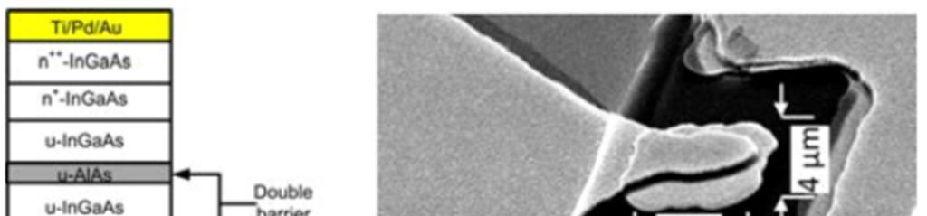
10 What is an RTD? RTD first demonstrated in 1974 Consists of vertical stacking of nanometric epitaxial layers of semiconductor alloys forming a double barrier quantum well (DBQW) Oscillations can be controlled by either electrical or optical signals Highly nonlinear device Complex behaviour including chaos. TypicalEpilayer Structure Lowest conduction band energy RTD Fabrication using BCB passivation/ planarisation Page 10
11 RTD technology Exhibit wideband Negative Differential Conductance (NDC) Fastest solid-state electronic oscillator at 1.55 THz (2014) Output power of 610 µw at 620 GHz has been reported (2013) Simple circuit realisation (photolithography works well up to 300 GHz) Current-Voltage(I-V) curve (NDC Negative Differential Conductance) Current Equivalent circuit NDC DC RTD Output AC Voltage negative Page 11

12 Taking advantage of RTD based communications: On-off keying modulation All-electronic RTD Optoelectronic RTD-PD Page 12

13 RTD with up to 30 GHz modulation (2015) f OSC = 350 GHz Y. Ikeda, S. Kitagawa, K. Okada, S. Suzuki, M. Asada, Direct intensity modulation of resonant-tunneling-diode terahertz oscillator up to ~30GHz IEICE Electronics Express 12, p (Jan-2015). Page 13

14 Potential of RTDs as THz Sources Simulated output power of a single RTD device oscillator Page 14

15 RTD THz source chip On-wafer characterisation of an RTD oscillator Measured spectrum of a fabricated 165 GHz RTD oscillator with record 0.35 mw output power Details to be presented at IEEE Compound Semiconductor IC Symposium CSICS 2015; Oct-2015; New Orleans, USA J. Wang, E. Wasige et al., "High Performance Resonant Tunnelling Diode Oscillators for THz applications" Page 15


16 Example of developed electronic RTD Page 16


17 Monolithic integration RTDs can be made of III-V semiconductor materials Typically employed in optoelectronic devices Allows for quasi-monolithic optoelectronic transceivers based on RTD-photodetectors and RTD-laser-modulators 1µm 3µm + Simple, compact and low cost built-in direct laser modulation Page 17


18 Example of developed optoelectronic RTD Page 18

19 ibrow workplan Page 19
20 ibrow methodology Baseline studies to establish application scenarios RTD technology options Channel modelling & communications architectures SWOT analysis Monolithic realisation of high power GHz GHz Low phase noise sources Ultimately on a III-V on Si platform Monolithic realisation of high responsivity (>0.6 A/W) and high sensitivity RTD-photodiode detectors Hybrid integration of RTD-PD and laser diode optical wireless interface and its characterisation Evaluation of wireless wireless links and optical wireless links Test bed demonstrator Page 20
21 Consortium organisation Electronic RTD design III-V on silicon Packaging Communications Optoelectronic RTD Design End-User Page 21
 Interface Si Substrate")

22 How to achieve low cost? III-V on silicon III-V epi (RTD/RTD-PD) Interface Si Substrate Direct growth of III-V RTD layers on a Si substrate Direct wafer bonding between III-V & Si substrates Potential for large diameter 200 mm wafers Integration with CMOS, etc. Page 22
23 III-V on silicon Conventional hybrid approaches, such as wire-bonded or flip-chip multi-chip assemblies suffer from variability and relative placement restrictions Direct hetero-epitaxial growth of III-V on a GeOI/Si template Exploit previous knowledge from the DARPA COSMOS programme Direct wafer bonding Process the III-V surface to achieve bonding at room temperature Proved effective in solving mismatch problems Lattice constant Thermal expansion coefficient. Page 23


24 RTD Packaging Thermal, mechanical and optical packaging design Hermetic sealing Lensed fibre coupling Page 24


25 Communication methods Channel modelling Test-bed for the demonstration of >10 Gbps wireless communications between several stand-alone prototype nodes at around 90 GHz and 300 GHz Page 25
26 Project Summary ibrow will achieve a novel RTD device technology: on a III-V on Si platform operating at millimetre-wave and terahertz frequencies integrated with laser diodes and photo-detectors A simple technology that can be integrated into both ends of a wireless link consumer portable devices fibre-optic supported base-stations. Page 26
Innovative ultra-broadband ubiquitous Wireless communications through terahertz transceivers ibrow
 Project Overview Innovative ultra-broadband ubiquitous Wireless communications through terahertz transceivers ibrow Mar-2017 Presentation outline Project key facts Motivation Project objectives Project
The resonant tunneling diode-laser diode optoelectronic integrated circuit operating as a voltage controlled oscillator
 The resonant tunneling diode-laser diode optoelectronic integrated circuit operating as a voltage controlled oscillator C. N. Ironside a, T. J. Slight a, L. Wang a and E. Wasige a, B. Romeira b and J.
Synchronization of Optically Coupled Resonant Tunneling Diode Oscillators
 Synchronization of ly Coupled Resonant Tunneling Diode Oscillators Bruno Romeira a, José M. L. Figueiredo a, Charles N. Ironside b, and José M. Quintana c a Centro de Electrónica, Optoelectrónica e Telecomunicações
Resonant tunneling diode optoelectronic integrated circuits
 Invited Paper Resonant tunneling diode optoelectronic integrated circuits C. N. Ironside a, J. M. L. Figueiredo b, B. Romeira b,t. J. Slight a, L. Wang a and E. Wasige a, a Department of Electronics and
Optoelectronic Oscillator Topologies based on Resonant Tunneling Diode Fiber Optic Links
 Optoelectronic Oscillator Topologies based on Resonant Tunneling Diode Fiber Optic Links Bruno Romeira* a, José M. L Figueiredo a, Kris Seunarine b, Charles N. Ironside b, a Department of Physics, CEOT,
TERAPOD. Terahertz based Ultra High Bandwidth Wireless Access Networks
 TERAPOD Terahertz based Ultra High Bandwidth Wireless Access Networks To investigate and demonstrate the feasibility of ultra high bandwidth wireless access networks operating in the Terahertz (THz) band.
Self-oscillation and period adding from a resonant tunnelling diode laser diode circuit
 Page 1 of 10 Self-oscillation and period adding from a resonant tunnelling diode laser diode circuit J. M. L. Figueiredo, B. Romeira, T. J. Slight, L. Wang, E. Wasige and C. N. Ironside A hybrid optoelectronic
Optoelectronic integrated circuits incorporating negative differential resistance devices
 Optoelectronic integrated circuits incorporating negative differential resistance devices José Figueiredo Centro de Electrónica, Optoelectrónica e Telecomunicações Departamento de Física da Faculdade de
Rights statement Post print of work supplied. Link to Publisher's website supplied in Alternative Location.
 Self-oscillation and period adding from resonant tunnelling diode-laser diode circuit Figueiredo, J. M. L., Romeira, B., Slight, T. J., Wang, L., Wasige, E., & Ironside, C. (2008). Self-oscillation and
Electronic-Photonic ICs for Low Cost and Scalable Datacenter Solutions
 Electronic-Photonic ICs for Low Cost and Scalable Datacenter Solutions Christoph Theiss, Director Packaging Christoph.Theiss@sicoya.com 1 SEMICON Europe 2016, October 27 2016 Sicoya Overview Spin-off from
Synchronizing optical to wireless signals using a resonant tunneling diode - laser diode circuit
 Synchronizing optical to wireless signals using a resonant tunneling diode - laser diode circuit B. Romeira, J. M. L. Figueiredo Centro de Electrónica, Optoelectrónica e Telecomunicações, Universidade
Recent Developments in Multifunctional Integration. Stephan Guttowski, Head of Technology Park»Heterointegration«, Fraunhofer FMD
 Recent Developments in Multifunctional Integration Stephan Guttowski, Head of Technology Park»Heterointegration«, Fraunhofer FMD Founding Participants 2 One-Stop-Shop for developments from wafer technologies
Heinrich-Hertz-Institut Berlin
 NOVEMBER 24-26, ECOLE POLYTECHNIQUE, PALAISEAU OPTICAL COUPLING OF SOI WAVEGUIDES AND III-V PHOTODETECTORS Ludwig Moerl Heinrich-Hertz-Institut Berlin Photonic Components Dept. Institute for Telecommunications,,
NEXT GENERATION SILICON PHOTONICS FOR COMPUTING AND COMMUNICATION PHILIPPE ABSIL
 NEXT GENERATION SILICON PHOTONICS FOR COMPUTING AND COMMUNICATION PHILIPPE ABSIL OUTLINE Introduction Platform Overview Device Library Overview What s Next? Conclusion OUTLINE Introduction Platform Overview
64 Channel Flip-Chip Mounted Selectively Oxidized GaAs VCSEL Array
 64 Channel Flip-Chip Mounted Selectively Oxidized GaAs VCSEL Array 69 64 Channel Flip-Chip Mounted Selectively Oxidized GaAs VCSEL Array Roland Jäger and Christian Jung We have designed and fabricated
 Wang, J., Al-Khalidi, A., Alharbi, K., Ofiare, A., Zhou, H., Wasige, E., and Figueiredo, J. (2017) High Performance Resonant Tunneling Diode Oscillators as Terahertz Sources. In: European Microwave Conference,
Silicon Photonics Technology Platform To Advance The Development Of Optical Interconnects
 Silicon Photonics Technology Platform To Advance The Development Of Optical Interconnects By Mieke Van Bavel, science editor, imec, Belgium; Joris Van Campenhout, imec, Belgium; Wim Bogaerts, imec s associated
A silicon avalanche photodetector fabricated with standard CMOS technology with over 1 THz gain-bandwidth product
 A silicon avalanche photodetector fabricated with standard CMOS technology with over 1 THz gain-bandwidth product Myung-Jae Lee and Woo-Young Choi* Department of Electrical and Electronic Engineering,
Silicon Photonics Transceivers for Hyper Scale Datacenters: Deployment and Roadmap
 Silicon Photonics Transceivers for Hyper Scale Datacenters: Deployment and Roadmap Peter De Dobbelaere Luxtera Inc. 09/19/2016 Luxtera Proprietary www.luxtera.com Luxtera Company Introduction $100B+ Shift
Quantum-effect Resonant Tunneling Device Technology for Practical Ultra Low-power High-speed Applications
 Quantum-effect Resonant Tunneling Device Technology for Practical Ultra Low-power High-speed Applications SEMATECH Symposium October 23 rd, 2012 Prof. Kyounghoon Yang High Speed Nanoelectronics Laboratory
Resonant Tunneling Device. Kalpesh Raval
 Resonant Tunneling Device Kalpesh Raval Outline Diode basics History of Tunnel diode RTD Characteristics & Operation Tunneling Requirements Various Heterostructures Fabrication Technique Challenges Application
Index. Cambridge University Press Silicon Photonics Design Lukas Chrostowski and Michael Hochberg. Index.
 absorption, 69 active tuning, 234 alignment, 394 396 apodization, 164 applications, 7 automated optical probe station, 389 397 avalanche detector, 268 back reflection, 164 band structures, 30 bandwidth
Low Thermal Resistance Flip-Chip Bonding of 850nm 2-D VCSEL Arrays Capable of 10 Gbit/s/ch Operation
 Low Thermal Resistance Flip-Chip Bonding of 85nm -D VCSEL Arrays Capable of 1 Gbit/s/ch Operation Hendrik Roscher In 3, our well established technology of flip-chip mounted -D 85 nm backside-emitting VCSEL
Integration of Optoelectronic and RF Devices for Applications in Optical Interconnect and Wireless Communication
 Integration of Optoelectronic and RF Devices for Applications in Optical Interconnect and Wireless Communication Zhaoran (Rena) Huang Assistant Professor Department of Electrical, Computer and System Engineering
IEEE JOURNAL OF SELECTED TOPICS IN QUANTUM ELECTRONICS 2010 Silicon Photonic Circuits: On-CMOS Integration, Fiber Optical Coupling, and Packaging
 IEEE JOURNAL OF SELECTED TOPICS IN QUANTUM ELECTRONICS 2010 Silicon Photonic Circuits: On-CMOS Integration, Fiber Optical Coupling, and Packaging Christophe Kopp, St ephane Bernab e, Badhise Ben Bakir,
Design and Modeling of Through-Silicon Vias for 3D Integration
 Design and Modeling of Through-Silicon Vias for 3D Integration Ivan Ndip, Brian Curran, Gerhard Fotheringham, Jurgen Wolf, Stephan Guttowski, Herbert Reichl Fraunhofer IZM & BeCAP @ TU Berlin IEEE Workshop
Simulation of High Resistivity (CMOS) Pixels
 Pixels") Simulation of High Resistivity (CMOS) Pixels Stefan Lauxtermann, Kadri Vural Sensor Creations Inc. AIDA-2020 CMOS Simulation Workshop May 13 th 2016 OUTLINE 1. Definition of High Resistivity Pixel Also
Simulation of High Resistivity (CMOS) Pixels Stefan Lauxtermann, Kadri Vural Sensor Creations Inc. AIDA-2020 CMOS Simulation Workshop May 13 th 2016 OUTLINE 1. Definition of High Resistivity Pixel Also
RFIC2017. Fully-Scalable 2D THz Radiating Array: A 42-Element Source in 130-nm SiGe with 80-μW Total Radiated Power at 1.01THz
 Student Paper Finalist Fully-Scalable 2D THz Radiating Array: A 42-Element Source in 130-nm SiGe with 80-μW Total Radiated Power at 1.01THz Zhi Hu and Ruonan Han MIT, Cambridge, MA, USA 1 Outline Motivation
ICT Micro- and nanoelectronics technologies
 EPoSS Proposers' Day, 2 Feb 2017, Brussels ICT 31-2017 Micro- and nanoelectronics technologies Eric Fribourg-Blanc, Henri Rajbenbach, Andreas Lymberis European Commission DG CONNECT (Communications Networks,
High Performance Mixed Signal Circuits Enabled by the Direct Monolithic Heterogeneous Integration of InP HBT and Si CMOS on a Silicon Substrate
 High Performance Mixed Signal Circuits Enabled by the Direct Monolithic Heterogeneous Integration of InP HBT and Si CMOS on a Silicon Substrate The MIT Faculty has made this article openly available. Please
Fundamentals of CMOS Image Sensors
 CHAPTER 2 Fundamentals of CMOS Image Sensors Mixed-Signal IC Design for Image Sensor 2-1 Outline Photoelectric Effect Photodetectors CMOS Image Sensor(CIS) Array Architecture CIS Peripherals Design Considerations
Si and InP Integration in the HELIOS project
 Si and InP Integration in the HELIOS project J.M. Fedeli CEA-LETI, Grenoble ( France) ECOC 2009 1 Basic information about HELIOS HELIOS photonics ELectronics functional Integration on CMOS www.helios-project.eu
Integrated Photonics using the POET Optical InterposerTM Platform
 Integrated Photonics using the POET Optical InterposerTM Platform Dr. Suresh Venkatesan CIOE Conference Shenzhen, China Sept. 5, 2018 POET Technologies Inc. TSXV: PUBLIC POET PTK.V Technologies Inc. PUBLIC
SNR characteristics of 850-nm OEIC receiver with a silicon avalanche photodetector
 SNR characteristics of 850-nm OEIC receiver with a silicon avalanche photodetector Jin-Sung Youn, 1 Myung-Jae Lee, 1 Kang-Yeob Park, 1 Holger Rücker, 2 and Woo-Young Choi 1,* 1 Department of Electrical
Ultra-low voltage resonant tunnelling diode electroabsorption modulator
 Ultra-low voltage resonant tunnelling diode electroabsorption modulator, 1/10 Ultra-low voltage resonant tunnelling diode electroabsorption modulator J. M. L. FIGUEIREDO Faculdade de Ciências e Tecnologia,
VERTICAL CAVITY SURFACE EMITTING LASER
 VERTICAL CAVITY SURFACE EMITTING LASER Nandhavel International University Bremen 1/14 Outline Laser action, optical cavity (Fabry Perot, DBR and DBF) What is VCSEL? How does VCSEL work? How is it different
Optoelectronic Oscillators for Communication Systems
 Optoelectronic Oscillators for Communication Systems Bruno Romeira and José Figueiredo Centro de Electrónica, Optoelectrónica e Telecomunicações Departamento de Física, Universidade do Algarve, 8005-139
SiNANO-NEREID Workshop:
 SiNANO-NEREID Workshop: Towards a new NanoElectronics Roadmap for Europe Leuven, September 11 th, 2017 WP3/Task 3.2 Connectivity RF and mmw Design Outline Connectivity, what connectivity? High data rates
Hetero Silicon Photonics: Components, systems, packaging and beyond
 Silicon Photonics Hetero Silicon Photonics: Components, systems, packaging and beyond Thursday, October 9, 2014 Tolga Tekin and Rifat Kisacik Photonic & Plasmonic Systems, Fraunhofer for Reliability and
Silicon Photonics Photo-Detector Announcement. Mario Paniccia Intel Fellow Director, Photonics Technology Lab
 Silicon Photonics Photo-Detector Announcement Mario Paniccia Intel Fellow Director, Photonics Technology Lab Agenda Intel s Silicon Photonics Research 40G Modulator Recap 40G Photodetector Announcement
Si CMOS Technical Working Group
 Si CMOS Technical Working Group CTR, Spring 2008 meeting Markets Interconnects TWG Breakouts Reception TWG reports Si CMOS: photonic integration E-P synergy - Integration - Standardization - Cross-market
The Past, Present, and Future of Silicon Photonics
 The Past, Present, and Future of Silicon Photonics Myung-Jae Lee High-Speed Circuits & Systems Lab. Dept. of Electrical and Electronic Engineering Yonsei University Outline Introduction A glance at history
Flexible Hybrid Electronics Fabricated with High-Performance COTS ICs using RTI CircuitFilm TM Technology
 Flexible Hybrid Electronics Fabricated with High-Performance COTS ICs using RTI CircuitFilm TM Technology Scott Goodwin 1, Erik Vick 2 and Dorota Temple 2 1 Micross Advanced Interconnect Technology Micross
Instruction manual and data sheet ipca h
 1/15 instruction manual ipca-21-05-1000-800-h Instruction manual and data sheet ipca-21-05-1000-800-h Broad area interdigital photoconductive THz antenna with microlens array and hyperhemispherical silicon
Jan Bogaerts imec
 imec 2007 1 Radiometric Performance Enhancement of APS 3 rd Microelectronic Presentation Days, Estec, March 7-8, 2007 Outline Introduction Backside illuminated APS detector Approach CMOS APS (readout)
Silicon Photonics: an Industrial Perspective
 Silicon Photonics: an Industrial Perspective Antonio Fincato Advanced Programs R&D, Cornaredo, Italy OUTLINE 2 Introduction Silicon Photonics Concept 300mm (12 ) Photonic Process Main Silicon Photonics
Winter 2017 Special Topics
 Winter 2017 Special Topics CRN Title Units Instructor Days/Time 22245 289K Terahertz and mm-wave Integrated Circuit Design 4 Momeni TR 4:40-6:00pm 45108 289L - Wide bandgap Semiconductor Devices (WBG-Devices)
According to this the work in the BRIDLE project was structured in the following work packages:
 The BRIDLE project: Publishable Summary (www.bridle.eu) The BRIDLE project sought to deliver a technological breakthrough in cost effective, high-brilliance diode lasers for industrial applications. Advantages
Special Issue Selected papers inspired by the Semiconductor and Integrated Optoelectronics (SIOE 2008) Conference ISSN
 Conference ISSN") Published in IET Optoelectronics Received on 28th April 2008 Revised on 28th July 2008 Special Issue Selected papers inspired by the Semiconductor and Integrated Optoelectronics (SIOE 2008) Conference
Published in IET Optoelectronics Received on 28th April 2008 Revised on 28th July 2008 Special Issue Selected papers inspired by the Semiconductor and Integrated Optoelectronics (SIOE 2008) Conference
Fabrication of antenna integrated UTC-PDs as THz sources
 Invited paper Fabrication of antenna integrated UTC-PDs as THz sources Siwei Sun 1, Tengyun Wang, Xiao xie 1, Lichen Zhang 1, Yuan Yao and Song Liang 1* 1 Key Laboratory of Semiconductor Materials Science,
Low-Cost Far-Infrared FPA based on High-Volume Pressure Sensor Process
 Low-Cost Far-Infrared FPA based on High-Volume Pressure Sensor Process Michael Krueger 1, Ingo Herrmann 1 Robert Bosch GmbH - Automotive Electronics, Tuebinger Str. 13, D-776 Reutlingen, Germany, michael.krueger@de.bosch.com
Job advertisement. Organisation/Company: Location: Research Field: Requirements 1 :
 We are one of the youngest universities in Germany and have a fresh way of looking at things. We think in terms of unlimited possibilities instead of possible limitations. Located in the heart of the Ruhr
Silicon Avalanche Photodiode SAR-/SARP-Series
 Silicon Avalanche Photodiode SAR-/SARP-Series DESCRIPTION The SAR500-Series is based on a reach-through structure for excellent quantum efficiency and high speed. The peak sensitivity in the NIR region
Design of THz Signal Generation Circuits Using 65nm CMOS Technologies
 Design of THz Signal Generation Circuits Using 65nm CMOS Technologies Hyeong-Jin Kim, Wonseok Choe, and Jinho Jeong Department of Electronics Engineering, Sogang University E-mail: jjeong@sogang.ac.kr
Figure Responsivity (A/W) Figure E E-09.
 Figure E E-09.") OSI Optoelectronics, is a leading manufacturer of fiber optic components for communication systems. The products offer range for Silicon, GaAs and InGaAs to full turnkey solutions. Photodiodes are semiconductor
OSI Optoelectronics, is a leading manufacturer of fiber optic components for communication systems. The products offer range for Silicon, GaAs and InGaAs to full turnkey solutions. Photodiodes are semiconductor
Lecture: Integration of silicon photonics with electronics. Prepared by Jean-Marc FEDELI CEA-LETI
 Lecture: Integration of silicon photonics with electronics Prepared by Jean-Marc FEDELI CEA-LETI Context The goal is to give optical functionalities to electronics integrated circuit (EIC) The objectives
Waveform Generators and Special function ICs UNIT-V
 Waveform Generators and Special function ICs UNIT-V There are basically two kinds of IC voltage regulators: Multipin type, e.g. LM723C 3-pin type, e.g. 78/79XX Multipin regulators are less popular
Hot Topics and Cool Ideas in Scaled CMOS Analog Design
 Engineering Insights 2006 Hot Topics and Cool Ideas in Scaled CMOS Analog Design C. Patrick Yue ECE, UCSB October 27, 2006 Slide 1 Our Research Focus High-speed analog and RF circuits Device modeling,
Silicon Photonics: A Platform for Integration, Wafer Level Assembly and Packaging
 Silicon Photonics: A Platform for Integration, Wafer Level Assembly and Packaging M. Asghari Kotura Inc April 27 Contents: Who is Kotura Choice of waveguide technology Challenges and merits of Si photonics
A Miniaturized Multi-Channel TR Module Design Based on Silicon Substrate
 Progress In Electromagnetics Research Letters, Vol. 74, 117 123, 2018 A Miniaturized Multi-Channel TR Module Design Based on Silicon Substrate Jun Zhou 1, 2, *, Jiapeng Yang 1, Donglei Zhao 1, and Dongsheng
New Wave SiP solution for Power
 New Wave SiP solution for Power Vincent Lin Corporate R&D ASE Group APEC March 7 th, 2018 in San Antonio, Texas. 0 Outline Challenges Facing Human Society Energy, Environment and Traffic Autonomous Driving
Measurements of Schottky-Diode Based THz Video Detectors
 Measurements of Schottky-Diode Based THz Video Detectors Hairui Liu 1, 2*, Junsheng Yu 1, Peter Huggard 2* and Byron Alderman 2 1 Beijing University of Posts and Telecommunications, Beijing, 100876, P.R.
FABULOUS. FDMA Access By Using Low-cost Optical network Units in Silicon photonics. S. Abrate
 FABULOUS FDMA Access By Using Low-cost Optical network Units in Silicon photonics S. Abrate 2 Project overview Project genesis FP7-ICT-2011-8 Objective 3.5: Core and disruptive photonic technologies Application-specific
Thermal Management in the 3D-SiP World of the Future
 Thermal Management in the 3D-SiP World of the Future Presented by W. R. Bottoms March 181 th, 2013 Smaller, More Powerful Portable Devices Are Driving Up Power Density Power (both power delivery and power
A 3.9 ns 8.9 mw 4 4 Silicon Photonic Switch Hybrid-Integrated with CMOS Driver
 A 3.9 ns 8.9 mw 4 4 Silicon Photonic Switch Hybrid-Integrated with CMOS Driver A. Rylyakov, C. Schow, B. Lee, W. Green, J. Van Campenhout, M. Yang, F. Doany, S. Assefa, C. Jahnes, J. Kash, Y. Vlasov IBM
Markets for On-Chip and Chip-to-Chip Optical Interconnects 2015 to 2024 January 2015
 Markets for On-Chip and Chip-to-Chip Optical Interconnects 2015 to 2024 January 2015 Chapter One: Introduction Page 1 1.1 Background to this Report CIR s last report on the chip-level optical interconnect
Si Photonics Technology Platform for High Speed Optical Interconnect. Peter De Dobbelaere 9/17/2012
 Si Photonics Technology Platform for High Speed Optical Interconnect Peter De Dobbelaere 9/17/2012 ECOC 2012 - Luxtera Proprietary www.luxtera.com Overview Luxtera: Introduction Silicon Photonics: Introduction
High-power flip-chip mounted photodiode array
 High-power flip-chip mounted photodiode array Allen S. Cross, * Qiugui Zhou, Andreas Beling, Yang Fu, and Joe C. Campbell Department of Electrical and Computer Engineering, University of Virginia, 351
MEDIA RELEASE FOR IMMEDIATE RELEASE 26 JULY 2016
 MEDIA RELEASE FOR IMMEDIATE RELEASE 26 JULY 2016 A*STAR S IME KICKS OFF CONSORTIA TO DEVELOP ADVANCED PACKAGING SOLUTIONS FOR NEXT-GENERATION INTERNET OF THINGS APPLICATIONS AND HIGH-PERFORMANCE WIRELESS
Integrated High Speed VCSELs for Bi-Directional Optical Interconnects
 Integrated High Speed VCSELs for Bi-Directional Optical Interconnects Volodymyr Lysak, Ki Soo Chang, Y ong Tak Lee (GIST, 1, Oryong-dong, Buk-gu, Gwangju 500-712, Korea, T el: +82-62-970-3129, Fax: +82-62-970-3128,
Examination Optoelectronic Communication Technology. April 11, Name: Student ID number: OCT1 1: OCT 2: OCT 3: OCT 4: Total: Grade:
 Examination Optoelectronic Communication Technology April, 26 Name: Student ID number: OCT : OCT 2: OCT 3: OCT 4: Total: Grade: Declaration of Consent I hereby agree to have my exam results published on
Special Issue Review. 1. Introduction
 Special Issue Review In recently years, we have introduced a new concept of photonic antennas for wireless communication system using radio-over-fiber technology. The photonic antenna is a functional device
Figure Figure E E-09. Dark Current (A) 1.
 1.") OSI Optoelectronics, is a leading manufacturer of fiber optic components for communication systems. The products offer range for Silicon, GaAs and InGaAs to full turnkey solutions. Photodiodes are semiconductor
OSI Optoelectronics, is a leading manufacturer of fiber optic components for communication systems. The products offer range for Silicon, GaAs and InGaAs to full turnkey solutions. Photodiodes are semiconductor
Millimeter- and Submillimeter-Wave Planar Varactor Sideband Generators
 Millimeter- and Submillimeter-Wave Planar Varactor Sideband Generators Haiyong Xu, Gerhard S. Schoenthal, Robert M. Weikle, Jeffrey L. Hesler, and Thomas W. Crowe Department of Electrical and Computer
Project: IEEE P Working Group for Wireless Personal Area Networks (WPANs)
") Project: IEEE P802.15 Working Group for Wireless Personal Area Networks (WPANs) Title: Feasibility test of THz channel for high-speed wireless link Date Submitted: 12 Nov 2013 Source: Jae-Young Kim, Ho-Jin
Project: IEEE P802.15 Working Group for Wireless Personal Area Networks (WPANs) Title: Feasibility test of THz channel for high-speed wireless link Date Submitted: 12 Nov 2013 Source: Jae-Young Kim, Ho-Jin
8-2 Stand-off Gas Sensing System Based on Terahertz Spectroscopy
 8-2 Stand-off Gas Sensing System Based on Terahertz Spectroscopy SHIMIZU Naofumi, FURUTA Tomofumi, KOHJIRO Satoshi, SUIZU Koji, KADO Yuichi, and KOMIYAMA Susumu We launched into a development of a new
MAPPER: High throughput Maskless Lithography
 MAPPER: High throughput Maskless Lithography Marco Wieland CEA- Leti Alterative Lithography workshop 1 Today s agenda Introduction Applications Qualification of on-tool metrology by in-resist metrology
RF MEMS for Low-Power Communications
 RF MEMS for Low-Power Communications Clark T.-C. Nguyen Center for Wireless Integrated Microsystems Dept. of Electrical Engineering and Computer Science University of Michigan Ann Arbor, Michigan 48109-2122
Fiber-Optic Transceivers for High-speed Digital Interconnects in Satellites
 Photo: ESA Fiber-Optic Transceivers for High-speed Digital Interconnects in Satellites ICSO conference, 9 Oct 2014 Mikko Karppinen (mikko.karppinen@vtt.fi), V. Heikkinen, K. Kautio, J. Ollila, A. Tanskanen
Negative Differential Resistance (NDR) Frequency Conversion with Gain
 Frequency Conversion with Gain") Third International Symposium on Space Tcrahertz Technology Page 457 Negative Differential Resistance (NDR) Frequency Conversion with Gain R. J. Hwu, R. W. Aim, and S. C. Lee Department of Electrical Engineering
Third International Symposium on Space Tcrahertz Technology Page 457 Negative Differential Resistance (NDR) Frequency Conversion with Gain R. J. Hwu, R. W. Aim, and S. C. Lee Department of Electrical Engineering
Millimeter-wave wireless R&D status in Panasonic and future research
 Millimeter-wave wireless R&D status in Panasonic and future research 4th Japan-EU Symposium 19 th January, 2012 Michiaki MATSUO Kazuaki TAKAHASHI Panasonic corporation Outline Panasonic s R&D activities
Detection of the mm-wave radiation using a low-cost LWIR microbolometer camera from a multiplied Schottky diode based source
 Detection of the mm-wave radiation using a low-cost LWIR microbolometer camera from a multiplied Schottky diode based source Basak Kebapci 1, Firat Tankut 2, Hakan Altan 3, and Tayfun Akin 1,2,4 1 METU-MEMS
This is a paper submitted to and accepted for publication in:
 This is a paper submitted to and accepted for publication in: Mu-Chieh Lo, Robinson Guzmán, Carlos Gordón and Guillermo Carpintero. Mode-locked photonic integrated circuits for millimeter and terahertz
Horizon 2020 and Photonics
 Brussels, 13 December 2013 Horizon 2020 and Photonics Thomas Skordas Head of the Photonics Unit, DG CONNECT European Commission Thomas.Skordas@ec.europa.eu Horizon 2020 Horizon 2020 Budget: 78.6 B (in
Vertical External Cavity Surface Emitting Laser
 Chapter 4 Optical-pumped Vertical External Cavity Surface Emitting Laser The booming laser techniques named VECSEL combine the flexibility of semiconductor band structure and advantages of solid-state
Guest Editorial of Special Issue on Software Defined Radio Transceivers and Circuits for 5G Wireless Communications
 IEEE Transactions on Circuits and Systems-II Guest Editorial of Special Issue on Software Defined Radio Transceivers and Circuits for 5G Wireless Communications W ireless communications is one of the fastest
Silicon Beam Lead Schottky Barrier Mixer Diodes
 ilicon chottky Barrier Mixer Diodes Features Ideal for MIC Low 1/f Noise Low Intermodulation Distortion Low Turn On Hermetically ealed Packages PC Controlled Wafer Fabrication Description Alpha beam lead
insert link to the published version of your paper
 Citation Niels Van Thienen, Wouter Steyaert, Yang Zhang, Patrick Reynaert, (215), On-chip and In-package Antennas for mm-wave CMOS Circuits Proceedings of the 9th European Conference on Antennas and Propagation
Flip-Chip for MM-Wave and Broadband Packaging
 1 Flip-Chip for MM-Wave and Broadband Packaging Wolfgang Heinrich Ferdinand-Braun-Institut für Höchstfrequenztechnik (FBH) Berlin / Germany with contributions by F. J. Schmückle Motivation Growing markets
Compact Solar Cell Ultra-Wideband Dipole Antenna
 Compact Solar Cell Ultra-Wideband Dipole Antenna Mina Danesh*, John R. Long High-Frequency Electronics Research Lab July 16, 2010 Delft University of Technology Challenge the future Outline Motivation
A 24-Channel 300 Gb/s 8.2 pj/bit Full-Duplex Fiber-Coupled Optical Transceiver Module Based on a Single Holey CMOS IC
 A 24-Channel 300 Gb/s 8.2 pj/bit Full-Duplex Fiber-Coupled Optical Transceiver Module Based on a Single Holey CMOS IC A. Rylyakov, C. Schow, F. Doany, B. Lee, C. Jahnes, Y. Kwark, C.Baks, D. Kuchta, J.
Direct intensity modulation of resonant-tunneling-diode terahertz oscillator up to ~30 GHz
 This article has been accepted and published on J-STAGE in advance of copyediting. Content is final as presented. IEICE Electronics Express, Vol.* No.*,*-* Direct intensity modulation of resonant-tunneling-diode
MYUNGHWAN PARK Westchester Park Drive, APT 1510, College Park, Maryland MOBILE : (+1) ,
 ,") RESEARCH INTERESTS MYUNGHWAN PARK 6200 Westchester Park Drive, APT 1510, College Park, Maryland 20740 MOBILE : (+1) 240-678-9863, EMAIL : mhpark@umd.edu My overall research interest is the physics of integrated
RESEARCH INTERESTS MYUNGHWAN PARK 6200 Westchester Park Drive, APT 1510, College Park, Maryland 20740 MOBILE : (+1) 240-678-9863, EMAIL : mhpark@umd.edu My overall research interest is the physics of integrated
Silicon Photonics for Mid-Board Optical Modules Marc Epitaux
 Silicon Photonics for Mid-Board Optical Modules Marc Epitaux Chief Architect at Samtec, Inc Outline Interconnect Solutions Mid-Board Optical Modules Silicon Photonics o Benefits o Challenges DragonFly
A NOVEL BIASED ANTI-PARALLEL SCHOTTKY DIODE STRUCTURE FOR SUBHARMONIC
 Page 342 A NOVEL BIASED ANTI-PARALLEL SCHOTTKY DIODE STRUCTURE FOR SUBHARMONIC Trong-Huang Lee', Chen-Yu Chi", Jack R. East', Gabriel M. Rebeiz', and George I. Haddad" let Propulsion Laboratory California
PAR4CR: THE DEVELOPMENT OF A NEW SDR-BASED PLATFORM TOWARDS COGNITIVE RADIO
 PAR4CR: THE DEVELOPMENT OF A NEW SDR-BASED PLATFORM TOWARDS COGNITIVE RADIO Olga Zlydareva Co-authors: Martha Suarez Rob Mestrom Fabian Riviere Outline 1 Introduction System Requirements Methodology System
Envisioning the Future of Optoelectronic Interconnects:
 Envisioning the Future of Optoelectronic Interconnects: The Production Economics of InP and Si Platforms for 100G Ethernet LAN Transceivers Shan Liu Dr. Erica Fuchs Prof. Randolph Kirchain MIT Microphotonics
High Speed pin Photodetector with Ultra-Wide Spectral Responses
 High Speed pin Photodetector with Ultra-Wide Spectral Responses C. Tam, C-J Chiang, M. Cao, M. Chen, M. Wong, A. Vazquez, J. Poon, K. Aihara, A. Chen, J. Frei, C. D. Johns, Ibrahim Kimukin, Achyut K. Dutta
Low-Power RF Integrated Circuit Design Techniques for Short-Range Wireless Connectivity
 Low-Power RF Integrated Circuit Design Techniques for Short-Range Wireless Connectivity Marvin Onabajo Assistant Professor Analog and Mixed-Signal Integrated Circuits (AMSIC) Research Laboratory Dept.
Photonic integrated circuit on InP for millimeter wave generation
 Invited Paper Photonic integrated circuit on InP for millimeter wave generation Frederic van Dijk 1, Marco Lamponi 1, Mourad Chtioui 2, François Lelarge 1, Gaël Kervella 1, Efthymios Rouvalis 3, Cyril