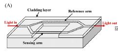
SPP waveguide sensors
|
|
|
- Mitchell Terry
- 5 years ago
- Views:
Transcription
1 SPP waveguide sensors 1. Optical sensor - Properties - Surface plasmon resonance sensor - Long-range surface plasmon-polariton sensor 2. LR-SPP waveguide - SPP properties in a waveguide - Asymmetric double-electrode waveguides - Basic ADW sensor structure with -fluidic channel 3. Proposed waveguide sensors - Influence of temperature fluctuation - LR-SPP waveguide index sensor - LR-SPP waveguide bio sensor
2 Contents Optical sensors 1. properties 2. Surface plasmon resonance sensor 3. Long-range surface plasmon-polariton sensor 2


3 1. properties Properties 1. Immune to electromagnetic interference 2. Capable of performing remote sensing 3. Provide multiplexed detection within a single device Source Measurement Detector 3
4 1. properties Fluorescence-based detection Label-free detection 4
5 2. Surface plasmon resonance sensor -Properties 1. Label free sensor (Real-time detection) 2. High sensitivity (Large filed enhancement at the interface between dielectric and metal) Prism is too bulky!!!! Difficult to integrate First SPR bio-sensing was demonstrated by Liedberg (1983) Commercial SPR sensor : RIU (Biacore TM ) Reference : Biosensors and Bioelectronics 23 (2007)
 1. Only penetrates into the surrounding medium for about 100 nm. Ref.")

6 2. Surface plasmon resonance sensor Other SPR sensor approaches (various SPP excitation method) 1. Only penetrates into the surrounding medium for about 100 nm. Ref. : Biosensors and Bioelectronics 23 (2007) How can sensitivity be increased? 3. Transmit both light signal and electrical signal? Metallic waveguide with Long-range surface plasmon mode 6
7 Contents LR-SPP waveguide 1. SPP properties in a metallic waveguide 2. Asymmetric double-electrode waveguides 3. Basic ADW sensor structure with -fluidic channel 7


8 1. SPP properties in a metallic waveguides Short-range surface plasmon mode Long-range surface plasmon mode 1. Highly enhanced electromagnetic field 2. High propagation loss. 1. Longer penetration depth into dielectric material 2. Low propagation loss. Therefore, LRSPP produce a narrower SPR features. Higher sensitivity!! 8

9 2. LRSPP waveguide sensors To use LRSPP mode and high Integration for a device. Solution : LRSPP metallic waveguide sensor!! Breakthrough : To excite a LRSPP mode, symmetry requirement is needed!! Dielectric Metal Dielectric The refractive index difference between two embedding materials should be lower than ~
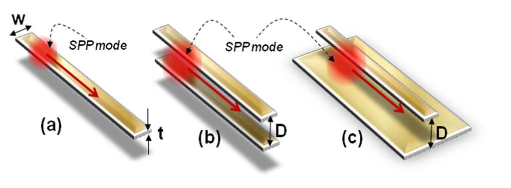


10 3. asymmetric double-electrode waveguides To overcome the symmetry requirement Metal (Au) -fluidic channle Substrate Substrate Substrate Metal (Au) 10


11 3. asymmetric double-electrode waveguides D metal strip d3 w 2 SPP mode Y-axis d1 D core d3 cladding Substrate metal slab X-axis 1. High degree of freedom of structure. (easy to apply to various applications) 2. Adjusting of core thickness, the symmetry requirement can overcome. 3. LRSPP mode is confined around the core layer. 4. Double metal layers for detecting bio-molecules. 5. Easily tuning the core dielectric layer by sending a current or voltage to double-electrodes 11
 (b) Propagation Loss (db/mm) 7.5 5.0 2.5 0.")
12 3. asymmetric double-electrode waveguides Cutoff Thickness "D c "(nm) Core 895 nm Core reflactive index ( ε 1 ) r k r k Core Thickness "D" (nm) (b) Propagation Loss (db/mm) (a) (1) (2) (3) Core Thickness "D" (nm) (c) 12
 코팅 Si d. PR patterning Si e. u coating Si f. PR lift-off Si g.")
13 3. asymmetric double-electrode waveguides - Fabrication process Si Si Si a. polymer ) 코팅 b. u coating c. polymer ) 코팅 Si d. PR patterning Si e. u coating Si f. PR lift-off Si g. polymer ) 코팅 13
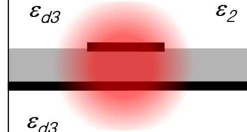

14 3. asymmetric double-electrode waveguides D metal strip SPP mode metal slab d3 w 2 Y-axis d1 D core d3 cladding X-axis 14


 width :5 μm,")
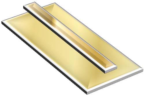
15 3. asymmetric double-electrode waveguides metal strip S-band metal slab Y-branch : mm 1.65mm 1mm : μm 20 μm 2mm 3mm 0.5mm <S-band> <Y-branch> Metal (Au) width :5 μm, Thickness:20nm Core thickness :680nm 15
16 3. asymmetric double-electrode waveguides 16
17 4. Basic ADW sensor structure with -fluidic channel Cladding Dielectric material Substrate Metal (Au) < Basic LR-SPP sensor structure > -fluidic channle Sensing Material Y Y Y Y Y Y Y Y Y Y Y Y Y Y Y Y Y Y Y Y Cladding Substrate Y Y Y Y Detection process ( protein ) Bio-molecule -Advantages of double LR-SPP bio-sensor structure 1. Reduced the size of the sensor structure comparing to the Kretschmann-reather configuration which use a prism. 2. Double LR-SPP structure can detect low index materials. ex) water, air, etc. 3. Easily excited the LR-SPP using end-fire coupling method with single mode fiber. 4. Double detecting metal layers. ( 1.5 times higher sensitivity then single metallic waveguide biosensor ) 5. Compensate the temperature fluctuation (self referencing). 17

18 4. Basic LRSPP sensor structure with -fluidic channel - Fabrication process Core layer coating 18


19 4. Basic LRSPP sensor structure with -fluidic channel y z x cladding y z core fluidic channel cladding gold slab silicon wafer cladding y cladding Si z cladding (b) cladding Si 19


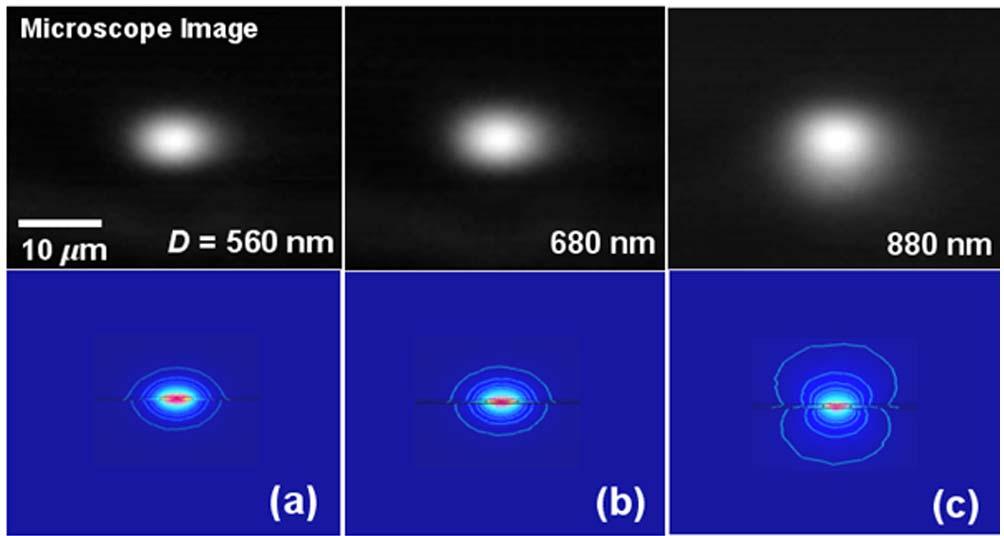
20 4. Basic LRSPP sensor structure with -fluidic channel Observing the LRSPP mode image 1. Inserting 1.45 index matching oil in the channel. 2. After 10 min inserting the matching oil, inserting an acetone ( n : 1.36 ) in the channel. 3. The LRSPP mode is gradually disappears Substrate n = 1.45 Index matching oil n = 1.36 acetone 10 m Cutoff Thickness "D c "(nm) nm nm 130 nm Core reflactive index ( ε 1 ) (a) Core 20
21 Contents Proposed waveguide sensors 1. Influence of temperature fluctuation 2. LR-SPP waveguide index sensor 3. LR-SPP waveguide bio sensor 21
 Thermal optic coefficient of aqueous solution for the solvent of the bio-molecules : -1 10-4 RIU/ C ~ 10-5 ~ 10-6 RIU (Sensitivity of SPR sensors) -Using reference channel for")
22 1. Influence of temperature fluctuation - To increase measurement accuracy Temperature fluctuations should be reduced!! ex ) Thermal optic coefficient of aqueous solution for the solvent of the bio-molecules : RIU/ C ~ 10-5 ~ 10-6 RIU (Sensitivity of SPR sensors) -Using reference channel for compensating temperature changes Ref : Proc. Of SPIE Vol
 Ref : IEEE Photonics Tech., Vol. 19, No. 24, 2007. 23")
23 1. Influence of temperature fluctuation Ref : Applied Optics, Vol. 41, No. 29, PP (2002) Ref : IEEE Photonics Tech., Vol. 19, No. 24,

24 1. Influence of temperature fluctuation - Other method to reduce temperature effects Ref : Measurement science and tech., Vol. 12, Ref : Sens. And Act. B., Vol. 134, pp. 854,

25 2. LR-SPP waveguide index sensor L R region : Detecting temperature changes L D region : Detecting refractive index changes of the bulk solutions. Claddings : n=1.47, thickness=15 m Bragg gratings : n=1.6, thickness=120 nm Core : n=1.46, thickness=700 nm period=528.8 nm Buffer layers : 300 nm wavelength : 1550 nm 25
26 2. LR-SPP waveguide index sensor - Fabrication process 1.47 polymer (15 m) Au coating ( 20nm ) Bragg grating (150nm /525.8nm) Buffer layer coating (250nm ) Core and Channel layer ( 500nm ) Buffer layer coating (250nm ) Au metal stripe (20nm, 5 m) 1.47 polymer (15 m) Removing the PR core layer 26


27 2. LR-SPP waveguide index sensor 0 OSA Tunable LD LRSPP sensor ASE broad source Polarizer 27
28 2. LR-SPP waveguide index sensor Transmittance (db) R TMM experiment D Transmittance (db) Wavelength (nm) Wavelength (nm) Measurement various bulk index solutions in the same sample. To detect other refractive index of the bulk solution, the inserted bulk solution was removed by methanol. Measurement order : ( 130 nm/riu ~10-6 RIU with 1 pm OSA resolution) 28
29 2. LR-SPP waveguide index sensor Transmittance (db) D R (nm) (c) Wavelength (nm) Sample index TMM experiment FWHM (nm) nm/riu ~10-6 RIU - D R = ± 540 pm ± 27 pm/k - R = ± 4.12 nm (with 1 pm OSA resolution and ± 20 K variation) - Thermal optic coefficient Polymer : RIU/K Sample oil : RIU/K D R (nm) (d) Temperature variation( K) 29 R (nm)


 bragg eff")
30 3. LR-SPP waveguide bio sensor y a. Before inserting bio-material with solution x z Cladding D c D g L w Substrate L L w Cladding y Bragg grating unit cell g Substrate z D c : core thickness ( 500 nm ) D g : grating depth t : bio-molecule thickness Solution Bio-molecule L g : grating length L g b. After inserting bio-material with solution Cladding D c ( n n ) bragg eff 1 eff 2 Cladding Substrate L g y z D g D g area D c area 575 nm 30


31 3. LR-SPP waveguide bio sensor - Two important properties of a bio-sensor 1. Sensitivity : The ratio of the change in sensor output to the change in the measurand. 2. Resolution : The smallest change in measurand which produces a detectable change in the sensor output. B Sensitivity, S, t : bio-molcule layer thickness t 10% FWHM 10% FWHM Resolution, tmin ( nm) t B S t Sensitivity, FWHM D g 31
32 3. LR-SPP waveguide bio sensor Sensitivity, S Grating depth, Dg (nm) Resolution, t min (nm) nm 40nm 60nm 80nm Grating length, Lg (mm) 1 nm Cladding 450 nm n cladding : 1.35, n core : 1.33 Bio-molecule : n protein (1.5), n solution : 1.33 Cladding Substrate L g y z D g Over 2 mm grating length (L g ), possible to detect under 1 nm thickness variation of bio-molecule layer (t) 32


 L w")

 2 2 2 Total")
 Propagation")

 = 10")
 Coupling efficiency ( c )")
 Propagation")
33 3. LR-SPP waveguide bio sensor < Experiment scheme of LR-SPP waveguide bio-sensor> Input signal Circulator Propagation efficiency ( w ) Maximum reflection ( R max ) L w Substrate L g L w Output signal L w Coupling efficiency ( c ) L g L w Propagation efficiency ( g ) Total Loss, T loss(db) = 10 log( c w g Rmax ) Propagation efficiency, η = P /P = 10 out in Propagation loss path length ( ) 10 where Propagation loss (db/mm) = 10 log (P /P ) out in Path length (mm) Coupling efficiency ( c ) : 80 % ( Overlap integral method ) Propagation efficiency ( w ) : 42 % ( at 450 nm core thickness with 1mm length ) 33
34 3. LR-SPP waveguide bio sensor Cladding Cladding L g y D g 450 nm constant Substrate z Total Loss, T loss(db) = 10 log( c w g Rmax ) g nm 40 nm 60 nm 80 nm Grating length, Lg (mm) Maximum reflection, R max Grating length, Lg (mm) 34
35 3. LR-SPP waveguide bio sensor Detectable range Total Loss "T loss " (db) nm 40nm 60nm 80nm Grating length, Lg (mm) Detectable limit line Resolution, t min (nm) nm 40nm 60nm 80nm 1 nm Grating length, Lg (mm) - Possible detecting grating length (L g ) is under 5.5 mm. - 1 nm thickness variation of the bio-molecule layer can be detected over 2 mm grating length (L g ). - Calculated minimum thickness variation of the bio-molecule layer is 0.36 nm at 40 nm grating depth.. 35
36 3. LR-SPP waveguide bio sensor y z x Cladding 450 nm -fluidic channel Bragg grating Cladding Substrate L g y z D g gold strip Cladding index : 1.35 Core index : 1.33 Grating period : 528 nm Wavelength : 1550 nm Index resolution ( x10 RIU) nm 40 nm 60 nm 80 nm grating length, L g (mm) Sample index : ~ The sensitivity increases as increasing the Bragg grating length or thickness ( ~ 10-6 RIU ) 36


37 3. LR-SPP waveguide bio sensor 37

38 6. Conclusion Proposing a novel model of LRSPP sensor on asymmetric double metallic structure. - Easy to excite the LRSPP mode using end-fire coupling method. - Still having the advantages of double metallic waveguide. - Easy to control the sensor properties adjusting the core thickness or grating depth. - Compensating temperature fluctuation (self-referencing) due to thermal-optic polymers. -~ 10-6 RIU (sensitivity), ± 27 pm/k (temperature inaccuracy) Possible to detect the under 1 nm thickness variation of a target bio-molecule layer. - Possible Bragg grating length under 30dB: 2 mm ~ 5.5 mm - Maximum detectable resolution is 0.36 nm 38
CHIRPED FIBER BRAGG GRATING (CFBG) BY ETCHING TECHNIQUE FOR SIMULTANEOUS TEMPERATURE AND REFRACTIVE INDEX SENSING
 BY ETCHING TECHNIQUE FOR SIMULTANEOUS TEMPERATURE AND REFRACTIVE INDEX SENSING") CHIRPED FIBER BRAGG GRATING (CFBG) BY ETCHING TECHNIQUE FOR SIMULTANEOUS TEMPERATURE AND REFRACTIVE INDEX SENSING Siti Aisyah bt. Ibrahim and Chong Wu Yi Photonics Research Center Department of Physics,
CHIRPED FIBER BRAGG GRATING (CFBG) BY ETCHING TECHNIQUE FOR SIMULTANEOUS TEMPERATURE AND REFRACTIVE INDEX SENSING Siti Aisyah bt. Ibrahim and Chong Wu Yi Photonics Research Center Department of Physics,
Microring-resonator-based sensor measuring both the concentration and temperature of a solution
 Microring-resonator-based sensor measuring both the concentration and temperature of a solution Min-Suk Kwon, 1,* and William H. Steier, 2 1 Department of Optical Engineering, Sejong University, 98 Gunja-dong,
Lecture 5. SPR Sensors: Principle and Instrumentation.
 Lecture 5 Optical sensors. SPR Sensors: Principle and Instrumentation. t ti Optical sensors What they can be based on: Absorption spectroscopy (UV-VIS, VIS IR) Fluorescence/phosphorescence spectroscopy
Realization of Polarization-Insensitive Optical Polymer Waveguide Devices
 644 Realization of Polarization-Insensitive Optical Polymer Waveguide Devices Kin Seng Chiang,* Sin Yip Cheng, Hau Ping Chan, Qing Liu, Kar Pong Lor, and Chi Kin Chow Department of Electronic Engineering,
Lecture 3. Mass sensors Optical sensors. SPR Sensors.
 Lecture 3 Mass sensors Optical sensors. SPR Sensors. Lecture plan mass sensors (QCM, SAW, u-cantilevers) thermal sensors optical sensors: adsorption diffractive index change SPR history concept performance
Localized biomolecular sensing enabled through plasmonic nanocavities
 Localized biomolecular sensing enabled through plasmonic nanocavities Gaël Osowiecki*, Elsie Barakat, Ali Naqavi, Hans Peter Herzig Optics & Photonics Technology Laboratory, École Polytechnique Fédérale
SENSITIVITY MODULATION OF SURFACE PLASMON RESONANCE SENSOR CONFIGURATIONS IN OPTICAL FIBER WAVEGUIDE
 Progress In Electromagnetics Research Letters, Vol. 37, 167 176, 2013 SENSITIVITY MODULATION OF SURFACE PLASMON RESONANCE SENSOR CONFIGURATIONS IN OPTICAL FIBER WAVEGUIDE Sushil Kumar, Gaurav Sharma, and
Optical RI sensor based on an in-fiber Bragg grating. Fabry-Perot cavity embedded with a micro-channel
 Optical RI sensor based on an in-fiber Bragg grating Fabry-Perot cavity embedded with a micro-channel Zhijun Yan *, Pouneh Saffari, Kaiming Zhou, Adedotun Adebay, Lin Zhang Photonic Research Group, Aston
Photonics and Optical Communication
 Photonics and Optical Communication (Course Number 300352) Spring 2007 Dr. Dietmar Knipp Assistant Professor of Electrical Engineering http://www.faculty.iu-bremen.de/dknipp/ 1 Photonics and Optical Communication
Fiber-Optic Surface Plasmon Resonance Sensor With Multi-Alternating Metal Layers for Biological Measurement
 Photonic Sensors (203) Vol. 3, No. 3: 202 207 DOI: 0.007/s3320-03-09-2 Regular Photonic Sensors Fiber-Optic Surface Plasmon Resonance Sensor With Multi-Alternating Metal Layers for Biological Measurement
Ultra-Low-Loss Athermal AWG Module with a Large Number of Channels
 Ultra-Low-Loss Athermal AWG Module with a Large Number of Channels by Junichi Hasegawa * and Kazutaka Nara * There is an urgent need for an arrayed waveguide grating (AWG), the device ABSTRACT that handles
A thin foil optical strain gage based on silicon-on-insulator microresonators
 A thin foil optical strain gage based on silicon-on-insulator microresonators D. Taillaert* a, W. Van Paepegem b, J. Vlekken c, R. Baets a a Photonics research group, Ghent University - INTEC, St-Pietersnieuwstraat
Terahertz Sensors Using Surface Waves in Periodic Metallic Structures
 Terahertz Sensors Using Surface Waves in Periodic Metallic Structures by Hadi Amarloo A thesis presented to the University of Waterloo in fulfillment of the thesis requirement for the degree of Master
Index. BaF 2 crystal 41 biochemical sensor 7, 316, ,
 Index acousto-optic effect 243 44 air bandedge 35, 266 air gap 188, 197, 224, 240 41 air holes 16 17, 52 53, 55, 64, 189, 192, 216 18, 241 43, 245, 266 68, 270 72, 298 99, 333 34, 336 37, 341 42 air pores
On-chip interrogation of a silicon-on-insulator microring resonator based ethanol vapor sensor with an arrayed waveguide grating (AWG) spectrometer
 spectrometer") On-chip interrogation of a silicon-on-insulator microring resonator based ethanol vapor sensor with an arrayed waveguide grating (AWG) spectrometer Nebiyu A. Yebo* a, Wim Bogaerts, Zeger Hens b,roel Baets
On-chip interrogation of a silicon-on-insulator microring resonator based ethanol vapor sensor with an arrayed waveguide grating (AWG) spectrometer Nebiyu A. Yebo* a, Wim Bogaerts, Zeger Hens b,roel Baets
Modeling of Gold Circular Sub-Wavelength Apertures on a Fiber Endface for Refractive Index Sensing
 (2012) Vol. 2, No. 3: 271 276 DOI: 10.1007/s13320-012-0068-1 Regular Modeling of Gold Circular Sub-Wavelength Apertures on a Fiber Endface for Refractive Index Sensing Huy NGUYEN 1, Gregory W. BAXTER 1*,
Characterization of Photonic Structures with CST Microwave Studio. CST UGM 2010 Darmstadt
 Characterization of Photonic Structures with CST Microwave Studio Stefan Prorok, Jan Hendrik Wülbern, Jan Hampe, Hooi Sing Lee, Alexander Petrov and Manfred Eich, Institute of Optical and Electronic Materials
Wavelength Division Multiplexing of a Fibre Bragg Grating Sensor using Transmit-Reflect Detection System
 Edith Cowan University Research Online ECU Publications 2012 2012 Wavelength Division Multiplexing of a Fibre Bragg Grating Sensor using Transmit-Reflect Detection System Gary Allwood Edith Cowan University
CHAPTER 2 POLARIZATION SPLITTER- ROTATOR BASED ON A DOUBLE- ETCHED DIRECTIONAL COUPLER
 CHAPTER 2 POLARIZATION SPLITTER- ROTATOR BASED ON A DOUBLE- ETCHED DIRECTIONAL COUPLER As we discussed in chapter 1, silicon photonics has received much attention in the last decade. The main reason is
Long-range surface plasmon polariton nanowire waveguides for device applications
 Long-range surface plasmon polariton nanowire waveguides for device applications K. Leosson, 1 T. Nikolajsen, 2 A. Boltasseva 3 and S. I. Bozhevolnyi 4 1 Science Institute, University of Iceland, Dunhagi
Opto-VLSI-based reconfigurable photonic RF filter
 Research Online ECU Publications 29 Opto-VLSI-based reconfigurable photonic RF filter Feng Xiao Mingya Shen Budi Juswardy Kamal Alameh This article was originally published as: Xiao, F., Shen, M., Juswardy,
Fiber-Optic Polarizer Using Resonant Tunneling through a Multilayer Overlay
 Fiber-Optic Polarizer Using Resonant Tunneling through a Multilayer Overlay Arun Kumar, Rajeev Jindal, and R. K. Varshney Department of Physics, Indian Institute of Technology, New Delhi 110 016 India
Design and Analysis of Resonant Leaky-mode Broadband Reflectors
 846 PIERS Proceedings, Cambridge, USA, July 6, 8 Design and Analysis of Resonant Leaky-mode Broadband Reflectors M. Shokooh-Saremi and R. Magnusson Department of Electrical and Computer Engineering, University
Impact of the light coupling on the sensing properties of photonic crystal cavity modes Kumar Saurav* a,b, Nicolas Le Thomas a,b,
 Impact of the light coupling on the sensing properties of photonic crystal cavity modes Kumar Saurav* a,b, Nicolas Le Thomas a,b, a Photonics Research Group, Ghent University-imec, Technologiepark-Zwijnaarde
UC Santa Barbara UC Santa Barbara Previously Published Works
 UC Santa Barbara UC Santa Barbara Previously Published Works Title Compact broadband polarizer based on shallowly-etched silicon-on-insulator ridge optical waveguides Permalink https://escholarship.org/uc/item/959523wq
Directional coupler (2 Students)
") Directional coupler (2 Students) The goal of this project is to make a 2 by 2 optical directional coupler with a defined power ratio for the two output branches. The directional coupler should be optimized
Directional coupler (2 Students) The goal of this project is to make a 2 by 2 optical directional coupler with a defined power ratio for the two output branches. The directional coupler should be optimized
Tunable Color Filters Based on Metal-Insulator-Metal Resonators
 Chapter 6 Tunable Color Filters Based on Metal-Insulator-Metal Resonators 6.1 Introduction In this chapter, we discuss the culmination of Chapters 3, 4, and 5. We report a method for filtering white light
Slot-waveguide Analysis and Fabrication of a Planar Dielectric Waveguide
 Slot-waveguide Analysis and Fabrication of a Planar Dielectric Waveguide Author: David Sánchez Gonzalo. Facultat de Física, Universitat de Barcelona, Diagonal 645, 08028 Barcelona, Spain*. Abstract: Waveguides
DWDM FILTERS; DESIGN AND IMPLEMENTATION
 DWDM FILTERS; DESIGN AND IMPLEMENTATION 1 OSI REFERENCE MODEL PHYSICAL OPTICAL FILTERS FOR DWDM SYSTEMS 2 AGENDA POINTS NEED CHARACTERISTICS CHARACTERISTICS CLASSIFICATION TYPES PRINCIPLES BRAGG GRATINGS
Title. Author(s)Fujisawa, Takeshi; Koshiba, Masanori. CitationOptics Letters, 31(1): Issue Date Doc URL. Rights. Type.
Fujisawa, Takeshi; Koshiba, Masanori. CitationOptics Letters, 31(1): Issue Date Doc URL. Rights. Type.") Title Polarization-independent optical directional coupler Author(s)Fujisawa, Takeshi; Koshiba, Masanori CitationOptics Letters, 31(1): 56-58 Issue Date 2006 Doc URL http://hdl.handle.net/2115/948 Rights
Title Polarization-independent optical directional coupler Author(s)Fujisawa, Takeshi; Koshiba, Masanori CitationOptics Letters, 31(1): 56-58 Issue Date 2006 Doc URL http://hdl.handle.net/2115/948 Rights
Waveguide Bragg Gratings and Resonators LUMERICAL SOLUTIONS INC
 Waveguide Bragg Gratings and Resonators JUNE 2016 1 Outline Introduction Waveguide Bragg gratings Background Simulation challenges and solutions Photolithography simulation Initial design with FDTD Band
Optically reconfigurable balanced dipole antenna
 Loughborough University Institutional Repository Optically reconfigurable balanced dipole antenna This item was submitted to Loughborough University's Institutional Repository by the/an author. Citation:
Polarization Analysis of an Asymmetrically Etched Rib Waveguide Coupler for Sensing Applications
 Photonic Sensors (2013) Vol. 3, No. 2: 178 183 DOI: 10.1007/s13320-013-0079-6 Regular Photonic Sensors Polarization Analysis of an Asymmetrically Etched Rib Waveguide Coupler for Sensing Applications Malathi
Module 16 : Integrated Optics I
 Module 16 : Integrated Optics I Lecture : Integrated Optics I Objectives In this lecture you will learn the following Introduction Electro-Optic Effect Optical Phase Modulator Optical Amplitude Modulator
High-power semiconductor lasers for applications requiring GHz linewidth source
 High-power semiconductor lasers for applications requiring GHz linewidth source Ivan Divliansky* a, Vadim Smirnov b, George Venus a, Alex Gourevitch a, Leonid Glebov a a CREOL/The College of Optics and
Title. Author(s)Saitoh, Fumiya; Saitoh, Kunimasa; Koshiba, Masanori. CitationOptics Express, 18(5): Issue Date Doc URL.
Saitoh, Fumiya; Saitoh, Kunimasa; Koshiba, Masanori. CitationOptics Express, 18(5): Issue Date Doc URL.") Title A design method of a fiber-based mode multi/demultip Author(s)Saitoh, Fumiya; Saitoh, Kunimasa; Koshiba, Masanori CitationOptics Express, 18(5): 4709-4716 Issue Date 2010-03-01 Doc URL http://hdl.handle.net/2115/46825
Title A design method of a fiber-based mode multi/demultip Author(s)Saitoh, Fumiya; Saitoh, Kunimasa; Koshiba, Masanori CitationOptics Express, 18(5): 4709-4716 Issue Date 2010-03-01 Doc URL http://hdl.handle.net/2115/46825
Study of multi physical parameter monitoring device based on FBG sensors demodulation system
 Advances in Engineering Research (AER), volume 116 International Conference on Communication and Electronic Information Engineering (CEIE 2016) Study of multi physical parameter monitoring device based
Optimization of a Love Wave Surface Acoustic Device for Biosensing Application
 Optimization of a Love Wave Surface Acoustic Device for Biosensing Application Yeswanth L Rao and Guigen Zhang Department of Biological & Agricultural Engineering University of Georgia Outline Introduction
Electronically tunable fabry-perot interferometers with double liquid crystal layers
 Electronically tunable fabry-perot interferometers with double liquid crystal layers Kuen-Cherng Lin *a, Kun-Yi Lee b, Cheng-Chih Lai c, Chin-Yu Chang c, and Sheng-Hsien Wong c a Dept. of Computer and
Silicon photonic devices based on binary blazed gratings
 Silicon photonic devices based on binary blazed gratings Zhiping Zhou Li Yu Optical Engineering 52(9), 091708 (September 2013) Silicon photonic devices based on binary blazed gratings Zhiping Zhou Li Yu
Bloch surface wave structures for high sensitivity detection and compact waveguiding
 Science and Technology of Advanced Materials ISSN: 1468-6996 (Print) 1878-5514 (Online) Journal homepage: http://tandfonline.com/loi/tsta20 Bloch surface wave structures for high sensitivity detection
High sensitivity SMS fiber structure based refractometer analysis and experiment
 High sensitivity SMS fiber structure based refractometer analysis and experiment Qiang Wu,* Yuliya Semenova, Pengfei Wang, and Gerald Farrell Photonics Research Centre, School of Electronic and Communications
Index. Cambridge University Press Silicon Photonics Design Lukas Chrostowski and Michael Hochberg. Index.
 absorption, 69 active tuning, 234 alignment, 394 396 apodization, 164 applications, 7 automated optical probe station, 389 397 avalanche detector, 268 back reflection, 164 band structures, 30 bandwidth
InP-based Waveguide Photodetector with Integrated Photon Multiplication
 InP-based Waveguide Photodetector with Integrated Photon Multiplication D.Pasquariello,J.Piprek,D.Lasaosa,andJ.E.Bowers Electrical and Computer Engineering Department University of California, Santa Barbara,
Compact hybrid TM-pass polarizer for silicon-on-insulator platform
 Compact hybrid TM-pass polarizer for silicon-on-insulator platform Muhammad Alam,* J. Stewart Aitchsion, and Mohammad Mojahedi Department of Electrical and Computer Engineering, University of Toronto,
Ratiometric Wavelength Monitor Based on Singlemode-Multimode-Singlemode Fiber Structure
 Dublin Institute of Technology ARROW@DIT Articles School of Electrical and Electronic Engineering 8-1-1 Ratiometric Wavelength Monitor Based on Singlemode-Multimode-Singlemode Fiber Structure Agus Hatta
Microphotonics Readiness for Commercial CMOS Manufacturing. Marco Romagnoli
 Microphotonics Readiness for Commercial CMOS Manufacturing Marco Romagnoli MicroPhotonics Consortium meeting MIT, Cambridge October 15 th, 2012 Passive optical structures based on SOI technology Building
A tunable Si CMOS photonic multiplexer/de-multiplexer
 A tunable Si CMOS photonic multiplexer/de-multiplexer OPTICS EXPRESS Published : 25 Feb 2010 MinJae Jung M.I.C.S Content 1. Introduction 2. CMOS photonic 1x4 Si ring multiplexer Principle of add/drop filter
AWG OPTICAL DEMULTIPLEXERS: FROM DESIGN TO CHIP. D. Seyringer
 AWG OPTICAL DEMULTIPLEXERS: FROM DESIGN TO CHIP D. Seyringer Research Centre for Microtechnology, Vorarlberg University of Applied Sciences, Hochschulstr. 1, 6850 Dornbirn, Austria, E-mail: dana.seyringer@fhv.at
A Low-loss Integrated Beam Combiner based on Polarization Multiplexing
 MITSUBISHI ELECTRIC RESEARCH LABORATORIES http://www.merl.com A Low-loss Integrated Beam Combiner based on Polarization Multiplexing Wang, B.; Kojima, K.; Koike-Akino, T.; Parsons, K.; Nishikawa, S.; Yagyu,
Simulation of technologically relevant SPR devices
 Simulation of technologically relevant SPR devices Author: Judith Costa Iracheta Advisor: Mauricio Moreno Sereno Facultat de Física, Universitat de Barcelona, Diagonal 645, 08028 Barcelona, Spain*. Abstract:
Horizontal single and multiple slot waveguides: optical transmission at λ = 1550 nm
 Horizontal single and multiple slot waveguides: optical transmission at λ = 1550 nm Rong Sun 1 *, Po Dong 2 *, Ning-ning Feng 1, Ching-yin Hong 1, Jurgen Michel 1, Michal Lipson 2, Lionel Kimerling 1 1Department
Rogério Nogueira Instituto de Telecomunicações Pólo de Aveiro Departamento de Física Universidade de Aveiro
 Fiber Bragg Gratings for DWDM Optical Networks Rogério Nogueira Instituto de Telecomunicações Pólo de Aveiro Departamento de Física Universidade de Aveiro Overview Introduction. Fabrication. Physical properties.
Propagation characteristics of hybrid modes supported by metal-low-high index waveguides and bends
 Propagation characteristics of hybrid modes supported by metal-low-high index waveguides and bends M. Z. Alam*, J. Meier, J. S. Aitchison, and M. Mojahedi Department of electrical and computer engineering,
Hybrid Integration Technology of Silicon Optical Waveguide and Electronic Circuit
 Hybrid Integration Technology of Silicon Optical Waveguide and Electronic Circuit Daisuke Shimura Kyoko Kotani Hiroyuki Takahashi Hideaki Okayama Hiroki Yaegashi Due to the proliferation of broadband services
We are IntechOpen, the world s leading publisher of Open Access books Built by scientists, for scientists. International authors and editors
 We are IntechOpen, the world s leading publisher of Open Access books Built by scientists, for scientists 3,900 116,000 120M Open access books available International authors and editors Downloads Our
 Chapter 5 5.1 What are the factors that determine the thickness of a polystyrene waveguide formed by spinning a solution of dissolved polystyrene onto a substrate? density of polymer concentration of polymer
ECE 6323 Ridge Waveguide Laser homework
 ECE 633 Ridge Waveguide Laser homework Introduction This is a slide from a lecture we will study later on. It is about diode lasers. Although we haven t studied diode lasers, there is one aspect about
Application Instruction 002. Superluminescent Light Emitting Diodes: Device Fundamentals and Reliability
 I. Introduction II. III. IV. SLED Fundamentals SLED Temperature Performance SLED and Optical Feedback V. Operation Stability, Reliability and Life VI. Summary InPhenix, Inc., 25 N. Mines Road, Livermore,
Design and Simulation of Optical Power Splitter By using SOI Material
 J. Pure Appl. & Ind. Phys. Vol.3 (3), 193-197 (2013) Design and Simulation of Optical Power Splitter By using SOI Material NAGARAJU PENDAM * and C P VARDHANI 1 * Research Scholar, Department of Physics,
Silicon Photonic Device Based on Bragg Grating Waveguide
 Silicon Photonic Device Based on Bragg Grating Waveguide Hwee-Gee Teo, 1 Ming-Bin Yu, 1 Guo-Qiang Lo, 1 Kazuhiro Goi, 2 Ken Sakuma, 2 Kensuke Ogawa, 2 Ning Guan, 2 and Yong-Tsong Tan 2 Silicon photonics
Silicon nitride based TriPleX Photonic Integrated Circuits for sensing applications
 Silicon nitride based TriPleX Photonic Integrated Circuits for sensing applications Arne Leinse a.leinse@lionix-int.com 2 Our chips drive your business 2 What are Photonic ICs (PICs)? Photonic Integrated
Guided Propagation Along the Optical Fiber
 Guided Propagation Along the Optical Fiber The Nature of Light Quantum Theory Light consists of small particles (photons) Wave Theory Light travels as a transverse electromagnetic wave Ray Theory Light
Photonic Crystal Slot Waveguide Spectrometer for Detection of Methane
 Photonic Crystal Slot Waveguide Spectrometer for Detection of Methane Swapnajit Chakravarty 1, Wei-Cheng Lai 2, Xiaolong (Alan) Wang 1, Che-Yun Lin 2, Ray T. Chen 1,2 1 Omega Optics, 10306 Sausalito Drive,
OPTI510R: Photonics. Khanh Kieu College of Optical Sciences, University of Arizona Meinel building R.626
 OPTI510R: Photonics Khanh Kieu College of Optical Sciences, University of Arizona kkieu@optics.arizona.edu Meinel building R.626 Announcements Homework #3 is due today No class Monday, Feb 26 Pre-record
Fabrication Techniques of Optical ICs
 Fabrication Techniques of Optical ICs Processing Techniques Lift off Process Etching Process Patterning Techniques Photo Lithography Electron Beam Lithography Photo Resist ( Microposit MP1300) Electron
Multimode interference demultiplexers and splitters in metal-insulator-metal waveguides
 Multimode interference demultiplexers and splitters in metal-insulator-metal waveguides Yao Kou and Xianfeng Chen* Department of Physics, The State Key Laboratory on Fiber Optic Local Area Communication
Development of a LFLE Double Pattern Process for TE Mode Photonic Devices. Mycahya Eggleston Advisor: Dr. Stephen Preble
 Development of a LFLE Double Pattern Process for TE Mode Photonic Devices Mycahya Eggleston Advisor: Dr. Stephen Preble 2 Introduction and Motivation Silicon Photonics Geometry, TE vs TM, Double Pattern
High Sensitivity Sensor Based on Porous Silicon Waveguide
 Mater. Res. Soc. Symp. Proc. Vol. 934 2006 Materials Research Society 0934-I10-04 High Sensitivity Sensor Based on Porous Silicon Waveguide Guoguang Rong 1, Jarkko J. Saarinen 2, John E. Sipe 2, and Sharon
E LECTROOPTICAL(EO)modulatorsarekeydevicesinoptical
modulatorsarekeydevicesinoptical") 286 JOURNAL OF LIGHTWAVE TECHNOLOGY, VOL. 26, NO. 2, JANUARY 15, 2008 Design and Fabrication of Sidewalls-Extended Electrode Configuration for Ridged Lithium Niobate Electrooptical Modulator Yi-Kuei Wu,
286 JOURNAL OF LIGHTWAVE TECHNOLOGY, VOL. 26, NO. 2, JANUARY 15, 2008 Design and Fabrication of Sidewalls-Extended Electrode Configuration for Ridged Lithium Niobate Electrooptical Modulator Yi-Kuei Wu,
Electromagnetically Induced Transparency with Hybrid Silicon-Plasmonic Travelling-Wave Resonators
 XXI International Workshop on Optical Wave & Waveguide Theory and Numerical Modelling 19-20 April 2013 Enschede, The Netherlands Session: Nanophotonics Electromagnetically Induced Transparency with Hybrid
Integrated electro-optical waveguide based devices with liquid crystals on a silicon backplane
 Integrated electro-optical waveguide based devices with liquid crystals on a silicon backplane Florenta Costache Group manager Smart Micro-Optics SMO/AMS Fraunhofer Institute for Photonic Microsystems,
Sensing platform based on micro-ring resonator and on-chip reference sensors in SOI
 Sensing platform based on micro-ring resonator and on-chip reference sensors in SOI S.M.C. Abdulla*, B.M. de Boer, J.M. Pozo, J.H. van den Berg, A. Abutan, R.A.J. Hagen, D.M.R. Lo Cascio, P. J. Harmsma
On-chip Si-based Bragg cladding waveguide with high index contrast bilayers
 On-chip Si-based Bragg cladding waveguide with high index contrast bilayers Yasha Yi, Shoji Akiyama, Peter Bermel, Xiaoman Duan, and L. C. Kimerling Massachusetts Institute of Technology, 77 Massachusetts
Optics Communications
 Optics Communications 283 (2010) 3678 3682 Contents lists available at ScienceDirect Optics Communications journal homepage: www.elsevier.com/locate/optcom Ultra-low-loss inverted taper coupler for silicon-on-insulator
True%Analog%Non-Mechanical%Beam%Steering%Using%Liquid%Crystal% Waveguide%Techniques%
 True%Analog%Non-Mechanical%Beam%Steering%Using%Liquid%Crystal% Waveguide%Techniques% Scott Davis, Scott Rommel, Mike Anderson, Derek Gann Vescent Photonics, 14998 W. 6 th Ave., Golden, CO 80401 The world
3D and Aerosol Printed Conductor Dielectric Full- 3D RF Metamaterials
 3D and Aerosol Printed Conductor Dielectric Full- 3D RF Metamaterials June 22, 2017 Jimmy Hester, Evan Nguyen, Jesse Tice, and Vesna Radisic Approved for Public Release: NG17-1180, 6/2/17 Outline Introduction
UNIT - 7 WDM CONCEPTS AND COMPONENTS
 UNIT - 7 WDM CONCEPTS AND COMPONENTS WDM concepts, overview of WDM operation principles, WDM standards, Mach-Zehender interferometer, multiplexer, Isolators and circulators, direct thin film filters, active
OPTICAL COMMUNICATIONS S
 OPTICAL COMMUNICATIONS S-108.3110 1 Course program 1. Introduction and Optical Fibers 2. Nonlinear Effects in Optical Fibers 3. Fiber-Optic Components 4. Transmitters and Receivers 5. Fiber-Optic Measurements
A novel tunable diode laser using volume holographic gratings
 A novel tunable diode laser using volume holographic gratings Christophe Moser *, Lawrence Ho and Frank Havermeyer Ondax, Inc. 85 E. Duarte Road, Monrovia, CA 9116, USA ABSTRACT We have developed a self-aligned
Ring resonator based SOI biosensors
 Ring resonator based SOI biosensors P. Bienstman a, S. Werquin a, C. Lerma Arce a, D. Witters b, R. Puers b, J. Lammertyn b, T. Claes a, E. Hallynck a, J.-W. Hoste a, D. Martens a a Ghent University, Photonics
S-band gain-clamped grating-based erbiumdoped fiber amplifier by forward optical feedback technique
 S-band gain-clamped grating-based erbiumdoped fiber amplifier by forward optical feedback technique Chien-Hung Yeh 1, *, Ming-Ching Lin 3, Ting-Tsan Huang 2, Kuei-Chu Hsu 2 Cheng-Hao Ko 2, and Sien Chi
Figure 1 Basic waveguide structure
 Recent Progress in SOI Nanophotonic Waveguides D. Van Thourhout, P. Dumon, W. Bogaerts, G. Roelkens, D. Taillaert, G. Priem, R. Baets IMEC-Ghent University, Department of Information Technology, St. Pietersnieuwstraat
Silicon photonics integration roadmap for applications in computing systems
 Silicon photonics integration roadmap for applications in computing systems Bert Jan Offrein Neuromorphic Devices and Systems Group 2016 IBM Corporation Outline Photonics and computing? The interconnect
Lecture: Integration of silicon photonics with electronics. Prepared by Jean-Marc FEDELI CEA-LETI
 Lecture: Integration of silicon photonics with electronics Prepared by Jean-Marc FEDELI CEA-LETI Context The goal is to give optical functionalities to electronics integrated circuit (EIC) The objectives
Analogical chromatic dispersion compensation
 Chapter 2 Analogical chromatic dispersion compensation 2.1. Introduction In the last chapter the most important techniques to compensate chromatic dispersion have been shown. Optical techniques are able
Surface-Emitting Single-Mode Quantum Cascade Lasers
 Surface-Emitting Single-Mode Quantum Cascade Lasers M. Austerer, C. Pflügl, W. Schrenk, S. Golka, G. Strasser Zentrum für Mikro- und Nanostrukturen, Technische Universität Wien, Floragasse 7, A-1040 Wien
Guided Propagation Along the Optical Fiber. Xavier Fernando Ryerson Comm. Lab
 Guided Propagation Along the Optical Fiber Xavier Fernando Ryerson Comm. Lab The Nature of Light Quantum Theory Light consists of small particles (photons) Wave Theory Light travels as a transverse electromagnetic
Department of Microelectronics, Faculty of Electrical Engineering, CTU, Prague Technicka 2, Prague 6, Czech Republic 2
 Ročník 2011 Číslo IV Design and Modeling of the ENR Polymer Microring Resonators Add/Drop Filter for Wavelength Division Multiplexing V. Prajzler 1, E. Strilek 1, I. Huttel 2, J. Spirkova 2, V. Jurka 3
Supporting Information
 Electronic Supplementary Material (ESI) for Materials Horizons. This journal is The Royal Society of Chemistry 2017 Supporting Information Nanofocusing of circularly polarized Bessel-type plasmon polaritons
Guided Propagation Along the Optical Fiber. Xavier Fernando Ryerson University
 Guided Propagation Along the Optical Fiber Xavier Fernando Ryerson University The Nature of Light Quantum Theory Light consists of small particles (photons) Wave Theory Light travels as a transverse electromagnetic
InP-based Waveguide Photodetector with Integrated Photon Multiplication
 InP-based Waveguide Photodetector with Integrated Photon Multiplication D.Pasquariello,J.Piprek,D.Lasaosa,andJ.E.Bowers Electrical and Computer Engineering Department University of California, Santa Barbara,
Design, Simulation & Optimization of 2D Photonic Crystal Power Splitter
 Optics and Photonics Journal, 2013, 3, 13-19 http://dx.doi.org/10.4236/opj.2013.32a002 Published Online June 2013 (http://www.scirp.org/journal/opj) Design, Simulation & Optimization of 2D Photonic Crystal
Waveguiding in PMMA photonic crystals
 ROMANIAN JOURNAL OF INFORMATION SCIENCE AND TECHNOLOGY Volume 12, Number 3, 2009, 308 316 Waveguiding in PMMA photonic crystals Daniela DRAGOMAN 1, Adrian DINESCU 2, Raluca MÜLLER2, Cristian KUSKO 2, Alex.
Design of athermal arrayed waveguide grating using silica/polymer hybrid materials
 Optica Applicata, Vol. XXXVII, No. 3, 27 Design of athermal arrayed waveguide grating using silica/polymer hybrid materials DE-LU LI, CHUN-SHENG MA *, ZHENG-KUN QIN, HAI-MING ZHANG, DA-MING ZHANG, SHI-YONG
Analysis and applications of 3D rectangular metallic waveguides
 Analysis and applications of 3D rectangular metallic waveguides Mohamed A. Swillam, and Amr S. Helmy Department of Electrical and Computer Engineering, University of Toronto, Toronto, M5S 3G4, Canada.
Novel Integrable Semiconductor Laser Diodes
 Novel Integrable Semiconductor Laser Diodes J.J. Coleman University of Illinois 1998-1999 Distinguished Lecturer Series IEEE Lasers and Electro-Optics Society Definition of the Problem Why aren t conventional
FINAL EXAM 12/12/03 EECS FALL 2003
 EECS 412 - FALL 2003 FINAL EXAM 12/12/03 NAME: CWRUnet e-mail address: IMPORTANT INFORMATION: 1. All questions are worth the same. 2. Exam is due December 12 th at 12 noon in Glennan 518. Possible 1. 10
DROPLET-LIKE BENT MULTIMODE FIBER SENSOR FOR TEMPERATURE AND REFRACTIVE INDEX MEASUREMENT
 DROPLET-LIKE BENT MULTIMODE FIBER SENSOR FOR TEMPERATURE AND REFRACTIVE INDEX MEASUREMENT N. Sidek 1, A. I. Azmi 1, M. A. A. Razak 2, M. R. Salim 1, A. S. Abdullah 1 and M. Y. Mohd Noor 1 1 Communication
Optical phase-locked loop for coherent transmission over 500 km using heterodyne detection with fiber lasers
 Optical phase-locked loop for coherent transmission over 500 km using heterodyne detection with fiber lasers Keisuke Kasai a), Jumpei Hongo, Masato Yoshida, and Masataka Nakazawa Research Institute of