Prepared by Dr. Ulkuhan Guler GT-Bionics Lab Georgia Institute of Technology
|
|
|
- Leon Preston
- 5 years ago
- Views:
Transcription


1 Prepared by Dr. Ulkuhan Guler GT-Bionics Lab Georgia Institute of Technology
2 OUTLINE Understanding Fabrication Imperfections Layout of MOS Transistor Matching Theory and Mismatches Device Matching, Interdigitation and Common Centroid Layouts Interconnections, Noise and Shielding System Layout, Floor planning, Clock Design
3 Digital and Analog Transistors Digital Speed Load Driving Capability Area Optimization Analog Accurate Aspect Ratio Matching Noise Minimize Stray and Gate Resistances


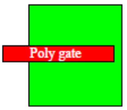
4 Layout and Real Chip is Different W S W 1 S 1
5 Possible Problems Related with Fabrication Mask Production / Misalignment Lateral Diffusion Over Etching / Undercut Boundary Conditions Non Uniformity 3 D Effects
6 Mask Misalignment
7 Mask Misalignment

8 Lateral Diffusion


9 Over Etching / Undercut Effect Boundary Dependent Etching

10 Etching Variations due to Different Contact Resistance
11 3 Dimensional Effects
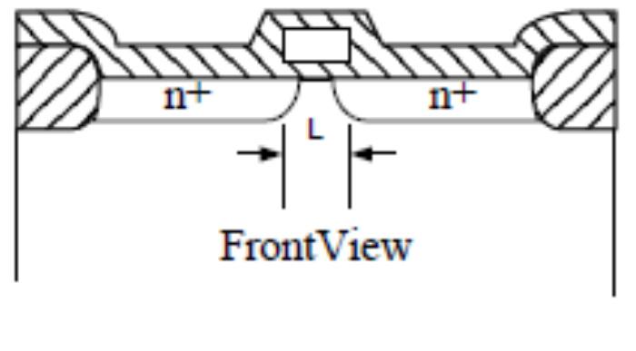
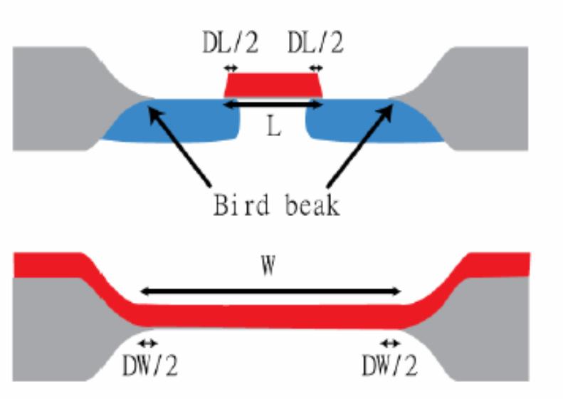
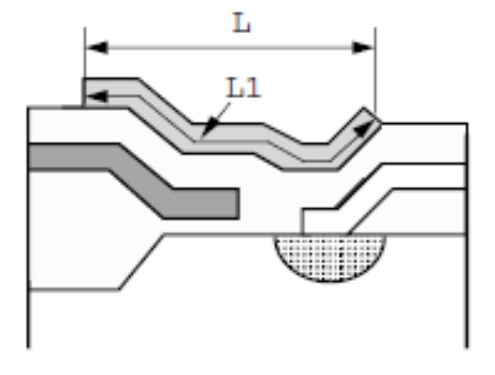
12 Difference between drawn and physical values
13 Outline Understanding Fabrication Imperfections Layout of MOS Transistor Matching Theory and Mismatches Device Matching, Interdigitation and Common Centroid Layouts Interconnections, Noise and Shielding System Layout, Floor planning, Clock Design

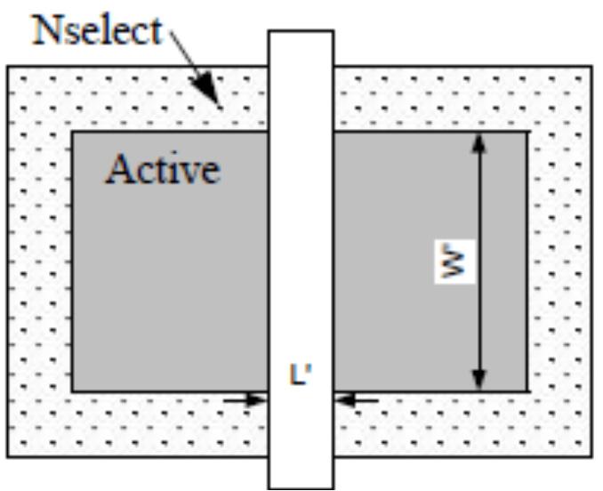
14 Forming NMOS and PMOS Transistors Ptap and Ntap is necessary to isolate transistors
15 Shallow Trench Isolation (STI)

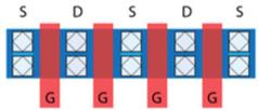
16 Proper NTAP and PTAP Connection

17 Proper NTAP and PTAP Connection

18 Source Drain Connection

19 Multiple or Single Contact Spiking

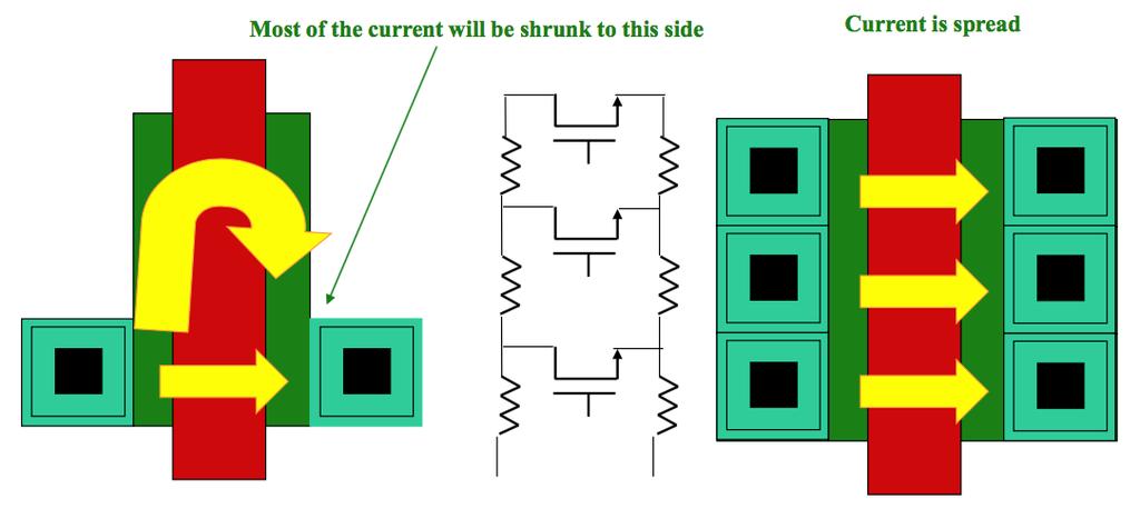
20 Analog Devices may have large W/L ratio Drain and source resistance are reduced with contacts Gate resistance is still high Drain Bulk and Source Bulk capacitance is still high Gate capacitance is still high Transistor Folding (Parallelization)
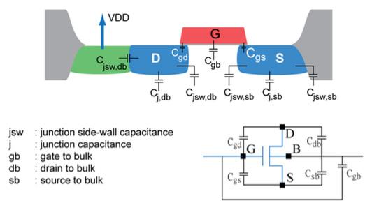
21 Parasitic Capacitances
22 Parasitic Resistances

23 Transistor Folding (Parallelization)

24 Transistor Folding (Parallelization) Gate Resistance Drain Bulk & Drain Source Capacitance
25 Outline Understanding Fabrication Imperfections Layout of MOS Transistor Matching Theory and Mismatches Device Matching, Interdigitation and Common Centroid Layouts Interconnections, Noise and Shielding System Layout, Floor planning, Clock Design
26 Mismatch Electrical properties of two devices are generally not same even they have the same layouts This is called as Mismatch Matching two devices is very important for some analog circuits such as, differential pair devices like opamp, and etc. Some kind of mismatches can not be modeled with simulation tools Designer should be aware of this during layout design


27 Effects of Mismatch on Performance Basic operation of some circuits directly depends on matching Common mode rejection is limited Eg. Current mirrors, Analog Digital Converter In differential pairs Supply noise rejection is limited In fully differential circuits Amplifier offset and/or load mismatch degrade the performance of some circuits which contain amplifier In digital circuits Eg. band gap, LDO Clock and signal skew and memory cell matchings
28 Mismatch M. J. M. Pelgrom, A. C. J. Duinmaijer, and A. P. G. Welbers, "Matching properties of MOS transistors," IEEE Journal of Solid State Circuits, vol. 24, pp , October Suppose two matched devices have parameters P1 and P2 Mismatched between these two devices is ΔP Mismatch has a Gaussian distribution, which has mean and standard deviation

29 Mismatch Systematic Mismatch Random Mismatch Mean µ(δp) Standard deviation σ(δp) Due to process variation Due to imperfect balancing in circuit and gradients Can not be eliminated totally but can be reduce significantly Can be minimized or even completely eliminated
30 Systematic Mismatch / Gradients Certain physical parameters such as temperature, process biases, mechanical stress, oxide thickness, poly silicon etch etc. may vary gradually across an IC. Since these variations can be computed mathematically, they are called as gradients. These variations can cause to systematic mismatches. Another reason of systematic mismatch is inadequate layout. Systematic mismatch can be very large and dominant. In some cases,a good way of testing systematic mismatch is power supply rejection simulation on the post layout netlist


31 Random Mismatch/Dopant Fluctuations Potential distribution of dopants in a 35nm MOSFET B.Cheng et al., The impact of random doping effects on CMOS SRAM cell, Proc. ESSCIRC, 2004, p B. Hoeneisen and C. A. Mead, Current voltage characteristics of small size MOS transistors, IEEE Trans. Electron Devices, vol. ED 19, pp , 1972
32 Random Mismatch/Pelgrom s Rule : : : : : 1 Place two devices closely 2 Apply Area Rule, increase WL

33 Random Mismatch / Some Analysis Big Transistors match better Jose Pineda de Gyvez and Hans P, Tuinhout, "Threshold Voltage Mismatch and Intra Die Leakage Current in Digital CMOS Circuits", JSSC, Vol. 39, no. I, pp , Jan Area Rule Brad Minch, 1999
34 Random Mismatch / Some Analysis

35 Why Matching?
36 Orientation Si and transistors are not perfectly isotropic Keep direction of current flow same

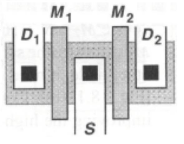
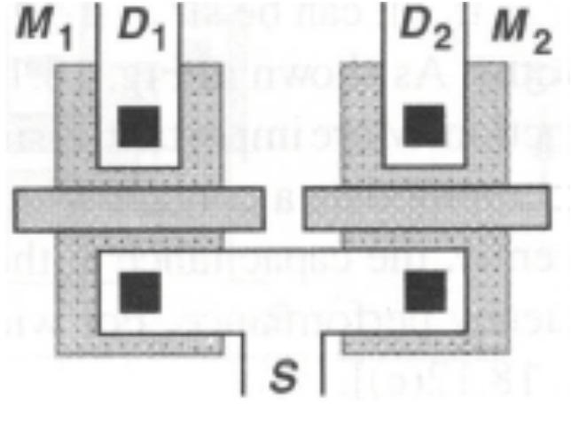
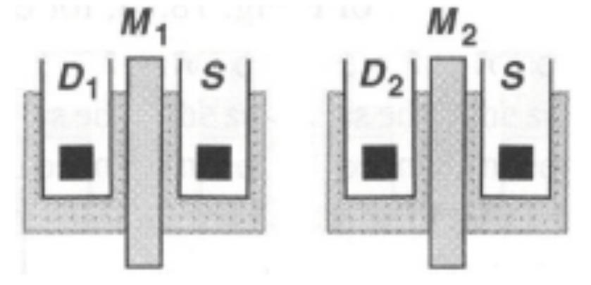
37 Exercise; Which layout?

38 Exercise; Which layout?

39 Exercise; Which layout? Dummy Device is added
40 Distance Effect Remember Pelgrom s Theorem, Place matched devices in close proximity


41 Over Etching/ Under cut Effect / Boundary Effect Use large W and L to reduce the effect of under cut Use dummy devices to provide same environment


42 Stress Effect There is also stress caused by metallization. Therefore do not route metal across active area, if routing is unavoidable add dummy metals so that each device sees same amount of metal
43 Oxide Thickness Devices with thinner oxide usually exhibit better matching Use minimum tox devices for best matching if the process offers a choice

44 Contacts Contacts in active gate region may cause variation in Vt. Gate contacts must be outside the active region to reduce dopant effects, stress, work function etc. Because of reliability issues use multiple contacts with exactly same number in the matched devices One contact resistance is around several ohms. Use multiple contacts reduce resistance.
45 Temperature effect Temperature gradients affect accuracy Devices need to be placed symmetrical with respect to power devices
46 Bias Effect Mismatch in the drain currents is bias dependent Vt mismatch has a larger effect at low bias levels. High Vgs V t is good for current matching. Try to keep Vds same. β mismatch dominates at high current M. J. M. Pelgrom, A. C. J. Duinmaijer, and A. P. G. Welbers, "Matching properties of MOS transistors," IEEE Journal of Solid State Circuits, vol. 24, pp , October um CMOS technology
47 Current Matching / / /2 Mismatch in the (W/L) values increase W/L Mismatch in the threshold values increase overdrive voltage
48 Voltage Matching 2 / / Threshold voltage mismatch can be reduced by careful layout Second component scaled with overdrive voltage, mismatch in the load and W/L Reduce overdrive voltage Increase W/L and RL
49 Current and Voltage Matching MOS transistors can be optimized either for voltage matching or for current matching, but not for both! For current matching keep overdrive voltage large (Current mirrors) For voltage matching keep overdrive voltage smaller (Differential pair devices) Route current a long way, not voltages. IR drops can cause big mismatches
50 Check List for Matching Place the transistors in close proximity Orient transistors in the same direction Place transistor s segments in the area of low stress gradients Place transistors away from the power devices Make current or voltage matching Use dummy devices if necessary Use multiple contacts Keep the layout of transistor compact Use Common Centroid layouts for critical devices

51 Corner Simulation Some of the manufacturing limitations (some systematic mismatches) are captured in the spice transistor models For example, two of the main parameters are DL and DW which show the differences between drawn and effective length and width of transistor, respectively. Manufacturing process tolerances of these parameters are emulated in the corner case simulations Narrower L and wider W Fast corner Wider L and smaller W Slow corner
52 Corner Simulation Some companies also provide models with fast NMOS and slow PMOS FS or with slow NMOS and fast PMOS SF Some companies want that the circuit work within 3 sigma spread is applied to typical corners FF3, SS um and smaller technologies requires models for leakage. Faster process, maximum supply voltage and maximum temperature ML Maximum Leakage Typical process, typical supply voltage and typical temperature TL Typical Leakage Monte Carlo Simulation can be run to center the design.
53 Tradeoffs Increased channel length Increased circuit area Increased power dissipation Reduced speed Determine required level of matching Minimal : 3σ 10mV, 3σ 2% Unit elements, matched orientation, compact layout Moderate : 3σ 2mV,3σ Apply most of layout rules Precise : Self calibration 0.1%
54 References A. Hastings, The Art of Analog Layout, 2nd Ed. Prentice Hall, Lee Eng Han, et. Al., CMOS Transistor Layout Kung Fu, utilities.com B. Razavi, Design of Analog CMOS Integrated Circuits, McGraw Hill, M. J. M. Pelgrom, A. C. J. Duinmaijer, and A. P. G. Welbers, "Matching properties of MOS transistors," IEEE Journal of Solid State Circuits, vol. 24, pp , October B.Cheng et al., The impact of random doping effects on CMOS SRAM cel1, Proc. ESSCIRC, 2004, p B. Hoeneisen and C. A. Mead, Current voltage characteristics of small size MOS transistors, IEEE Trans. Electron Devices, vol. ED 19, pp , 1972 Jose Pineda de Gyvez and Hans P, Tuinhout, "Threshold Voltage Mismatch and Intra Die Leakage Current in Digital CMOS Circuits", JSSC, Vol. 39, no. I, pp , Jan M. F. Lan et. al., Current Mirror Layout Strategies for Enhancing Matching Performance, Kluwer AICSP, July D. Clein, CMOS IC Layout Concepts, Methodologies, and Tools, Boston, 1999.D. Clein, CMOS IC Layout Concepts, Methodologies, and Tools, Boston, J. Franca and Y. Tsividis, editors, Design of Analog Digital VLSI Circuits For Telecommunications and Signal Processing, 2nd Ed., Prentice Hall, 1994.


55 References M. Ismail and T. Fiez editors, Analog VLSI Signal and Information Processing, McGraw Hill, M. F. Lan et. al., Current Mirror Layout Strategies for Enhancing Matching Performance, Kluwer AICSP, July F. Maloberti, Analog Design for CMOS VLSI Systems, Springer US S. Palermo, Analog VLSI Circuit Design Course Slides S. Hu, Clock Network Synthesis Course Slides Delbruck, Indiveri, Liu, Transistor Mismatch and Layout Techniques Mai, alon, Labonte, Analog Layout H. Luong, Analog Layout Techniques B. Boser, Device Matching Mechanisms F. Yuan, Analog CMOS Integrated Circuits Course, MOS Device Layout Techniques Slides J. Ghosh, Advanced VLSI Design Lab, Layout of Analog Circuits Slides H. Aboushady, CMOS Process Technology Course Slides G. Wang, Layout for Analog Circuits
18-Mar-08. Lecture 5, Transistor matching and good layout techniques
 Transistor mismatch & Layout techniques 1. Transistor mismatch its causes and how to estimate its magnitude 2. Layout techniques for good matching 3. Layout techniques to minimize parasitic effects Part
Bridging the Gap between Dreams and Nano-Scale Reality
 Bridging the Gap between Dreams and Nano-Scale Reality Ban P. Wong Design Methodology, Chartered Semiconductor wongb@charteredsemi.com 28 July 2006 Outline Deficiencies in Boolean-based Design Rules in
PROCESS and environment parameter variations in scaled
 1078 IEEE TRANSACTIONS ON CIRCUITS AND SYSTEMS II: EXPRESS BRIEFS, VOL. 53, NO. 10, OCTOBER 2006 Reversed Temperature-Dependent Propagation Delay Characteristics in Nanometer CMOS Circuits Ranjith Kumar
444 Index. F Fermi potential, 146 FGMOS transistor, 20 23, 57, 83, 84, 98, 205, 208, 213, 215, 216, 241, 242, 251, 280, 311, 318, 332, 354, 407
 Index A Accuracy active resistor structures, 46, 323, 328, 329, 341, 344, 360 computational circuits, 171 differential amplifiers, 30, 31 exponential circuits, 285, 291, 292 multifunctional structures,
Semiconductor Memory: DRAM and SRAM. Department of Electrical and Computer Engineering, National University of Singapore
 Semiconductor Memory: DRAM and SRAM Outline Introduction Random Access Memory (RAM) DRAM SRAM Non-volatile memory UV EPROM EEPROM Flash memory SONOS memory QD memory Introduction Slow memories Magnetic
Variation-Aware Design for Nanometer Generation LSI
 HIRATA Morihisa, SHIMIZU Takashi, YAMADA Kenta Abstract Advancement in the microfabrication of semiconductor chips has made the variations and layout-dependent fluctuations of transistor characteristics
A 7 bit 3.52 GHz Current Steering DAC for WiGig Applications
 A 7 bit 3.52 GHz Current Steering DAC for WiGig Applications Trindade, M. Helena Abstract This paper presents a Digital to Analog Converter (DAC) with 7 bit resolution and a sampling rate of 3.52 GHz to
STATISTICAL DESIGN AND YIELD ENHANCEMENT OF LOW VOLTAGE CMOS ANALOG VLSI CIRCUITS
 STATISTICAL DESIGN AND YIELD ENHANCEMENT OF LOW VOLTAGE CMOS ANALOG VLSI CIRCUITS Istanbul Technical University Electronics and Communications Engineering Department Tuna B. Tarim Prof. Dr. Hakan Kuntman
Modeling and CAD Challenges for DFY. Patrick G. Drennan Freescale Semiconductor Tempe, AZ, USA
 Modeling and CAD Challenges for DFY Patrick G. Drennan Freescale Semiconductor Tempe, AZ, USA Outline Unphysical casing and statistical models Process gradients Gate protect diodes Shallow trench isolation
3084 IEEE TRANSACTIONS ON NUCLEAR SCIENCE, VOL. 60, NO. 4, AUGUST 2013
 3084 IEEE TRANSACTIONS ON NUCLEAR SCIENCE, VOL. 60, NO. 4, AUGUST 2013 Dummy Gate-Assisted n-mosfet Layout for a Radiation-Tolerant Integrated Circuit Min Su Lee and Hee Chul Lee Abstract A dummy gate-assisted
Outline. Layout and technology. CMOS technology Design rules Analog layout Mismatch INF4420. Jørgen Andreas Michaelsen Spring / 80 2 / 80
 INF4420 Layout and technology Jørgen Andreas Michaelsen Spring 2013 1 / 80 Outline CMOS technology Design rules Analog layout Mismatch Spring 2013 Layout and technology 2 2 / 80 Introduction As circuit
Introduction to VLSI ASIC Design and Technology
 Introduction to VLSI ASIC Design and Technology Paulo Moreira CERN - Geneva, Switzerland Paulo Moreira Introduction 1 Outline Introduction Is there a limit? Transistors CMOS building blocks Parasitics
Fabrication, Corner, Layout, Matching, & etc.
 Advanced Analog Building Blocks Fabrication, Corner, Layout, Matching, & etc. Wei SHEN (KIP) 1 Fabrication Steps for MOS Wei SHEN, Universität Heidelberg 2 Fabrication Steps for MOS Wei SHEN, Universität
Layout and technology
 INF4420 Layout and technology Dag T. Wisland Spring 2015 Outline CMOS technology Design rules Analog layout Mismatch Spring 2015 Layout and technology 2 Introduction As circuit designers we must carefully
ECE 546 Lecture 12 Integrated Circuits
 ECE 546 Lecture 12 Integrated Circuits Spring 2018 Jose E. Schutt-Aine Electrical & Computer Engineering University of Illinois jesa@illinois.edu ECE 546 Jose Schutt Aine 1 Integrated Circuits IC Requirements
DIGITALLY controlled and area-efficient calibration circuits
 246 IEEE TRANSACTIONS ON CIRCUITS AND SYSTEMS II: EXPRESS BRIEFS, VOL. 52, NO. 5, MAY 2005 A Low-Voltage 10-Bit CMOS DAC in 0.01-mm 2 Die Area Brandon Greenley, Raymond Veith, Dong-Young Chang, and Un-Ku
On-Chip Transistor Characterization Arrays with Digital Interfaces for Variability Characterization *
 On-Chip Transistor Characterization Arrays with Digital Interfaces for Variability Characterization * Simeon Realov, William McLaughlin, K. L. Shepard Department of Electrical Engineering, Columbia University
Jack Keil Wolf Lecture. ESE 570: Digital Integrated Circuits and VLSI Fundamentals. Lecture Outline. MOSFET N-Type, P-Type.
 ESE 570: Digital Integrated Circuits and VLSI Fundamentals Jack Keil Wolf Lecture Lec 3: January 24, 2019 MOS Fabrication pt. 2: Design Rules and Layout http://www.ese.upenn.edu/about-ese/events/wolf.php
Reducing Transistor Variability For High Performance Low Power Chips
 Reducing Transistor Variability For High Performance Low Power Chips HOT Chips 24 Dr Robert Rogenmoser Senior Vice President Product Development & Engineering 1 HotChips 2012 Copyright 2011 SuVolta, Inc.
AS THE semiconductor process is scaled down, the thickness
 IEEE TRANSACTIONS ON CIRCUITS AND SYSTEMS II: EXPRESS BRIEFS, VOL. 52, NO. 7, JULY 2005 361 A New Schmitt Trigger Circuit in a 0.13-m 1/2.5-V CMOS Process to Receive 3.3-V Input Signals Shih-Lun Chen,
FinFET-based Design for Robust Nanoscale SRAM
 FinFET-based Design for Robust Nanoscale SRAM Prof. Tsu-Jae King Liu Dept. of Electrical Engineering and Computer Sciences University of California at Berkeley Acknowledgements Prof. Bora Nikoli Zheng
ECEN 474/704 Lab 6: Differential Pairs
 ECEN 474/704 Lab 6: Differential Pairs Objective Design, simulate and layout various differential pairs used in different types of differential amplifiers such as operational transconductance amplifiers
ESE 570: Digital Integrated Circuits and VLSI Fundamentals
 ESE 570: Digital Integrated Circuits and VLSI Fundamentals Lec 3: January 24, 2019 MOS Fabrication pt. 2: Design Rules and Layout Penn ESE 570 Spring 2019 Khanna Jack Keil Wolf Lecture http://www.ese.upenn.edu/about-ese/events/wolf.php
45nm Bulk CMOS Within-Die Variations. Courtesy of C. Spanos (UC Berkeley) Lecture 11. Process-induced Variability I: Random
 Lecture 11. Process-induced Variability I: Random") 45nm Bulk CMOS Within-Die Variations. Courtesy of C. Spanos (UC Berkeley) Lecture 11 Process-induced Variability I: Random Random Variability Sources and Characterization Comparisons of Different MOSFET
45nm Bulk CMOS Within-Die Variations. Courtesy of C. Spanos (UC Berkeley) Lecture 11 Process-induced Variability I: Random Random Variability Sources and Characterization Comparisons of Different MOSFET
Lecture 11: Clocking
 High Speed CMOS VLSI Design Lecture 11: Clocking (c) 1997 David Harris 1.0 Introduction We have seen that generating and distributing clocks with little skew is essential to high speed circuit design.
Design of Nano-Electro Mechanical (NEM) Relay Based Nano Transistor for Power Efficient VLSI Circuits
 Relay Based Nano Transistor for Power Efficient VLSI Circuits") Design of Nano-Electro Mechanical (NEM) Relay Based Nano Transistor for Power Efficient VLSI Circuits Arul C 1 and Dr. Omkumar S 2 1 Research Scholar, SCSVMV University, Kancheepuram, India. 2 Associate
Design of Nano-Electro Mechanical (NEM) Relay Based Nano Transistor for Power Efficient VLSI Circuits Arul C 1 and Dr. Omkumar S 2 1 Research Scholar, SCSVMV University, Kancheepuram, India. 2 Associate
Temperature-adaptive voltage tuning for enhanced energy efficiency in ultra-low-voltage circuits
 Microelectronics Journal 39 (2008) 1714 1727 www.elsevier.com/locate/mejo Temperature-adaptive voltage tuning for enhanced energy efficiency in ultra-low-voltage circuits Ranjith Kumar, Volkan Kursun Department
Fin-Shaped Field Effect Transistor (FinFET) Min Ku Kim 03/07/2018
 Min Ku Kim 03/07/2018") Fin-Shaped Field Effect Transistor (FinFET) Min Ku Kim 03/07/2018 ECE 658 Sp 2018 Semiconductor Materials and Device Characterizations OUTLINE Background FinFET Future Roadmap Keeping up w/ Moore s Law
Fin-Shaped Field Effect Transistor (FinFET) Min Ku Kim 03/07/2018 ECE 658 Sp 2018 Semiconductor Materials and Device Characterizations OUTLINE Background FinFET Future Roadmap Keeping up w/ Moore s Law
Design Analysis and Performance Comparison of Low Power High Gain 2nd Stage Differential Amplifier Along with 1st Stage
 Design Analysis and Performance Comparison of Low Power High Gain 2nd Stage Differential Amplifier Along with 1st Stage Sadeque Reza Khan Department of Electronic and Communication Engineering, National
IMPROVED CURRENT MIRROR OUTPUT PERFORMANCE BY USING GRADED-CHANNEL SOI NMOSFETS
 IMPROVED CURRENT MIRROR OUTPUT PERFORMANCE BY USING GRADED-CHANNEL SOI NMOSFETS Marcelo Antonio Pavanello *, João Antonio Martino and Denis Flandre 1 Laboratório de Sistemas Integráveis Escola Politécnica
A Low Power Low Voltage High Performance CMOS Current Mirror
 RESEARCH ARTICLE OPEN ACCESS A Low Power Low Voltage High Performance CMOS Current Mirror Sirish Rao, Sampath Kumar V Department of Electronics & Communication JSS Academy of Technical Education Noida,
ECEN474/704: (Analog) VLSI Circuit Design Fall 2016
 VLSI Circuit Design Fall 2016") ECEN474/704: (Analog) VLSI Circuit Design Fall 2016 Lecture 1: Introduction Sam Palermo Analog & Mixed-Signal Center Texas A&M University Announcements Turn in your 0.18um NDA form by Thursday Sep 1 No
ECEN474/704: (Analog) VLSI Circuit Design Fall 2016 Lecture 1: Introduction Sam Palermo Analog & Mixed-Signal Center Texas A&M University Announcements Turn in your 0.18um NDA form by Thursday Sep 1 No
Low-Power VLSI. Seong-Ook Jung VLSI SYSTEM LAB, YONSEI University School of Electrical & Electronic Engineering
 Low-Power VLSI Seong-Ook Jung 2013. 5. 27. sjung@yonsei.ac.kr VLSI SYSTEM LAB, YONSEI University School of Electrical & Electronic Engineering Contents 1. Introduction 2. Power classification & Power performance
ECE 5745 Complex Digital ASIC Design Topic 2: CMOS Devices
 ECE 5745 Complex Digital ASIC Design Topic 2: CMOS Devices Christopher Batten School of Electrical and Computer Engineering Cornell University http://www.csl.cornell.edu/courses/ece5950 Simple Transistor
CHAPTER 8 DIFFERENTIAL AND MULTISTAGE AMPLIFIERS
 CHAPTER 8 DIFFERENTIAL AND MULTISTAGE AMPLIFIERS Chapter Outline 8.1 The CMOS Differential Pair 8. Small-Signal Operations of the MOS Differential Pair 8.3 The BJT Differential Pair 8.4 Other Non-ideal
An Improved Bandgap Reference (BGR) Circuit with Constant Voltage and Current Outputs
 Circuit with Constant Voltage and Current Outputs") International Journal of Research in Engineering and Innovation Vol-1, Issue-6 (2017), 60-64 International Journal of Research in Engineering and Innovation (IJREI) journal home page: http://www.ijrei.com
International Journal of Research in Engineering and Innovation Vol-1, Issue-6 (2017), 60-64 International Journal of Research in Engineering and Innovation (IJREI) journal home page: http://www.ijrei.com
Introduction to CMOS VLSI Design (E158) Lecture 9: Cell Design
 Lecture 9: Cell Design") Harris Introduction to CMOS VLSI Design (E158) Lecture 9: Cell Design David Harris Harvey Mudd College David_Harris@hmc.edu Based on EE271 developed by Mark Horowitz, Stanford University MAH E158 Lecture
Harris Introduction to CMOS VLSI Design (E158) Lecture 9: Cell Design David Harris Harvey Mudd College David_Harris@hmc.edu Based on EE271 developed by Mark Horowitz, Stanford University MAH E158 Lecture
Analog IC Design. Lecture 1,2: Introduction & MOS transistors. Henrik Sjöland. Dept. of Electrical and Information Technology
 Analog IC Design Lecture 1,2: Introduction & MOS transistors Henrik.Sjoland@eit.lth.se Part 1: Introduction Analogue IC Design (7.5hp, lp2) CMOS Technology Analog building blocks in CMOS Single- and multiple
Basic Layout Techniques
 Basic Layout Techniques Rahul Shukla Advisor: Jaime Ramirez-Angulo Spring 2005 Mixed Signal VLSI Lab Klipsch School of Electrical and Computer Engineering New Mexico State University Outline Transistor
Design and Layout of Two Stage High Bandwidth Operational Amplifier
 Design and Layout of Two Stage High Bandwidth Operational Amplifier Yasir Mahmood Qureshi Abstract This paper presents the design and layout of a two stage, high speed operational amplifiers using standard
Low Transistor Variability The Key to Energy Efficient ICs
 Low Transistor Variability The Key to Energy Efficient ICs 2 nd Berkeley Symposium on Energy Efficient Electronic Systems 11/3/11 Robert Rogenmoser, PhD 1 BEES_roro_G_111103 Copyright 2011 SuVolta, Inc.
PROCESS-VOLTAGE-TEMPERATURE (PVT) VARIATIONS AND STATIC TIMING ANALYSIS
 VARIATIONS AND STATIC TIMING ANALYSIS") PROCESS-VOLTAGE-TEMPERATURE (PVT) VARIATIONS AND STATIC TIMING ANALYSIS The major design challenges of ASIC design consist of microscopic issues and macroscopic issues [1]. The microscopic issues are ultra-high
PROCESS-VOLTAGE-TEMPERATURE (PVT) VARIATIONS AND STATIC TIMING ANALYSIS The major design challenges of ASIC design consist of microscopic issues and macroscopic issues [1]. The microscopic issues are ultra-high
Analyzing Combined Impacts of Parameter Variations and BTI in Nano-scale Logical Gates
 Analyzing Combined Impacts of Parameter Variations and BTI in Nano-scale Logical Gates Seyab Khan Said Hamdioui Abstract Bias Temperature Instability (BTI) and parameter variations are threats to reliability
TECHNO INDIA BATANAGAR (DEPARTMENT OF ELECTRONICS & COMMUNICATION ENGINEERING) QUESTION BANK- 2018
 QUESTION BANK- 2018") TECHNO INDIA BATANAGAR (DEPARTMENT OF ELECTRONICS & COMMUNICATION ENGINEERING) QUESTION BANK- 2018 Paper Setter Detail Name Designation Mobile No. E-mail ID Raina Modak Assistant Professor 6290025725 raina.modak@tib.edu.in
TECHNO INDIA BATANAGAR (DEPARTMENT OF ELECTRONICS & COMMUNICATION ENGINEERING) QUESTION BANK- 2018 Paper Setter Detail Name Designation Mobile No. E-mail ID Raina Modak Assistant Professor 6290025725 raina.modak@tib.edu.in
! Review: MOS IV Curves and Switch Model. ! MOS Device Layout. ! Inverter Layout. ! Gate Layout and Stick Diagrams. ! Design Rules. !
 ESE 570: Digital Integrated Circuits and VLSI Fundamentals Lec 3: January 21, 2016 MOS Fabrication pt. 2: Design Rules and Layout Lecture Outline! Review: MOS IV Curves and Switch Model! MOS Device Layout!
ESE 570: Digital Integrated Circuits and VLSI Fundamentals
 ESE 570: Digital Integrated Circuits and VLSI Fundamentals Lec 3: January 21, 2016 MOS Fabrication pt. 2: Design Rules and Layout Penn ESE 570 Spring 2016 Khanna Adapted from GATech ESE3060 Slides Lecture
A 2V Rail-to-Rail Micropower CMOS Comparator.
 A 2V Rail-to-Rail Micropower CMOS Comparator. M. Barú, O. de Oliveira, F. Silveira. Instituto de Ingeniería Eléctrica Universidad de la República Casilla de Correos 30 Montevideo, Uruguay. Tel: +598 2
Lecture 9: Cell Design Issues
 Lecture 9: Cell Design Issues MAH, AEN EE271 Lecture 9 1 Overview Reading W&E 6.3 to 6.3.6 - FPGA, Gate Array, and Std Cell design W&E 5.3 - Cell design Introduction This lecture will look at some of the
! Review: MOS IV Curves and Switch Model. ! MOS Device Layout. ! Inverter Layout. ! Gate Layout and Stick Diagrams. ! Design Rules. !
 ESE 570: Digital Integrated Circuits and VLSI Fundamentals Lec 3: January 21, 2017 MOS Fabrication pt. 2: Design Rules and Layout Lecture Outline! Review: MOS IV Curves and Switch Model! MOS Device Layout!
Low-Power and Process Variation Tolerant Memories in sub-90nm Technologies
 Low-Power and Process Variation Tolerant Memories in sub-9nm Technologies Saibal Mukhopadhyay, Swaroop Ghosh, Keejong Kim, and Kaushik Roy Dept. of ECE, Purdue University, West Lafayette, IN, @ecn.purdue.edu
Performance Modeling, Parameter Extraction Technique and Statistical Modeling of Nano-scale MOSFET for VLSI Circuit Simulation
 Performance Modeling, Parameter Extraction Technique and Statistical Modeling of Nano-scale MOSFET for VLSI Circuit Simulation Dr. Soumya Pandit Institute of Radio Physics and Electronics University of
Session 3: Solid State Devices. Silicon on Insulator
 Session 3: Solid State Devices Silicon on Insulator 1 Outline A B C D E F G H I J 2 Outline Ref: Taurand Ning 3 SOI Technology SOl materials: SIMOX, BESOl, and Smart Cut SIMOX : Synthesis by IMplanted
Electrical Characterization of a Second-gate in a Silicon-on-Insulator Transistor
 Electrical Characterization of a Second-gate in a Silicon-on-Insulator Transistor Antonio Oblea: McNair Scholar Dr. Stephen Parke: Faculty Mentor Electrical Engineering As an independent double-gate, silicon-on-insulator
Study of Differential Amplifier using CMOS
 Study of Differential Amplifier using CMOS Mr. Bhushan Bangadkar PG Scholar Mr. Amit Lamba Assistant Professor Mr. Vipin Bhure Assistant Professor Electronics and Communication Electronics and Communication
CMOS Scaling and Variability
 WIMNACT WS & IEEE EDS Mini-colloquim on Nano-CMOS Technology January 3, 212, TITECH, Japan CMOS Scaling and Variability 212. 1. 3 NEC Tohru Mogami WIMNACT WS 212, January 3, Titech 1 Acknowledgements I
Variable Body Biasing Technique to Reduce Leakage Current in 4x4 DRAM in VLSI
 Variable Body Biasing Technique to Reduce Leakage Current in 4x4 DRAM in VLSI A.Karthik 1, K.Manasa 2 Assistant Professor, Department of Electronics and Communication Engineering, Narsimha Reddy Engineering
MOSFET & IC Basics - GATE Problems (Part - I)
") MOSFET & IC Basics - GATE Problems (Part - I) 1. Channel current is reduced on application of a more positive voltage to the GATE of the depletion mode n channel MOSFET. (True/False) [GATE 1994: 1 Mark]
MOSFET & IC Basics - GATE Problems (Part - I) 1. Channel current is reduced on application of a more positive voltage to the GATE of the depletion mode n channel MOSFET. (True/False) [GATE 1994: 1 Mark]
Design of Analog CMOS Integrated Circuits
 Design of Analog CMOS Integrated Circuits Behzad Razavi Professor of Electrical Engineering University of California, Los Angeles H Boston Burr Ridge, IL Dubuque, IA Madison, WI New York San Francisco
Semiconductor TCAD Tools
 Device Design Consideration for Nanoscale MOSFET Using Semiconductor TCAD Tools Teoh Chin Hong and Razali Ismail Department of Microelectronics and Computer Engineering, Universiti Teknologi Malaysia,
CHAPTER 2 THE DESIGN OF ACTIVE POLYPHASE FILTER
 CHAPTER 2 THE DESIGN OF ACTIVE POLYPHASE FILTER 2.1 INTRODUCTION The fast growth of wireless applications in recent years has driven intense efforts to design highly integrated, high-performance, low-cost
MANY integrated circuit applications require a unique
 IEEE JOURNAL OF SOLID-STATE CIRCUITS, VOL. 43, NO. 1, JANUARY 2008 69 A Digital 1.6 pj/bit Chip Identification Circuit Using Process Variations Ying Su, Jeremy Holleman, Student Member, IEEE, and Brian
Technology, Jabalpur, India 1 2
 1181 LAYOUT DESIGNING AND OPTIMIZATION TECHNIQUES USED FOR DIFFERENT FULL ADDER TOPOLOGIES ARPAN SINGH RAJPUT 1, RAJESH PARASHAR 2 1 M.Tech. Scholar, 2 Assistant professor, Department of Electronics and
ALow Voltage Wide-Input-Range Bulk-Input CMOS OTA
 Analog Integrated Circuits and Signal Processing, 43, 127 136, 2005 c 2005 Springer Science + Business Media, Inc. Manufactured in The Netherlands. ALow Voltage Wide-Input-Range Bulk-Input CMOS OTA IVAN
Chapter 1. Introduction
 EECS3611 Analog Integrated Circuit esign Chapter 1 Introduction EECS3611 Analog Integrated Circuit esign Instructor: Prof. Ebrahim Ghafar-Zadeh, Prof. Peter Lian email: egz@cse.yorku.ca peterlian@cse.yorku.ca
FUNDAMENTALS OF MODERN VLSI DEVICES
 19-13- FUNDAMENTALS OF MODERN VLSI DEVICES YUAN TAUR TAK H. MING CAMBRIDGE UNIVERSITY PRESS Physical Constants and Unit Conversions List of Symbols Preface page xi xiii xxi 1 INTRODUCTION I 1.1 Evolution
Topic 3. CMOS Fabrication Process
 Topic 3 CMOS Fabrication Process Peter Cheung Department of Electrical & Electronic Engineering Imperial College London URL: www.ee.ic.ac.uk/pcheung/ E-mail: p.cheung@ic.ac.uk Lecture 3-1 Layout of a Inverter
PHYSICAL STRUCTURE OF CMOS INTEGRATED CIRCUITS. Dr. Mohammed M. Farag
 PHYSICAL STRUCTURE OF CMOS INTEGRATED CIRCUITS Dr. Mohammed M. Farag Outline Integrated Circuit Layers MOSFETs CMOS Layers Designing FET Arrays EE 432 VLSI Modeling and Design 2 Integrated Circuit Layers
Dual Metal Gate and Conventional MOSFET at Sub nm for Analog Application
 Dual Metal Gate and Conventional MOSFET at Sub nm for Analog Application Sonal Aggarwal 1 and Rajbir Singh 2 1 Department of Electronic Science, Kurukshetra university,kurukshetra sonal.aggarwal88@gmail.com
Tuesday, March 22nd, 9:15 11:00
 Nonlinearity it and mismatch Tuesday, March 22nd, 9:15 11:00 Snorre Aunet (sa@ifi.uio.no) Nanoelectronics group Department of Informatics University of Oslo Last time and today, Tuesday 22nd of March:
Design of Robust CMOS Amplifiers Combining Advanced Low-Voltage and Feedback Techniques
 Design of Robust CMOS Amplifiers Combining Advanced Low-Voltage and Feedback Techniques Somayeh Abdollahvand, António Gomes, David Rodrigues, Fábio Januário and João Goes Centre for Technologies and Systems
VLSI Based Design of Low Power and Linear CMOS Temperature Sensor
 VLSI Based Design of Low Power and Linear CMOS Temperature Sensor Poorvi Jain 1, Pramod Kumar Jain 2 1 Research Scholar (M.Teh), Department of Electronics and Instrumentation,SGSIS, Indore 2 Associate
Dr. Ralf Sommer. Munich, March 8th, 2006 COM BTS DAT DF AMF. Presenter Dept Titel presentation Date Page 1
 DATE 2006 Special Session: DFM/DFY Design for Manufacturability and Yield - Influence of Process Variations in Digital, Analog and Mixed-Signal Circuit Design DATE 06 Munich, March 8th, 2006 Presenter
Power MOSFET Zheng Yang (ERF 3017,
 ECE442 Power Semiconductor Devices and Integrated Circuits Power MOSFET Zheng Yang (ERF 3017, email: yangzhen@uic.edu) Evolution of low-voltage (
On Chip Active Decoupling Capacitors for Supply Noise Reduction for Power Gating and Dynamic Dual Vdd Circuits in Digital VLSI
 ELEN 689 606 Techniques for Layout Synthesis and Simulation in EDA Project Report On Chip Active Decoupling Capacitors for Supply Noise Reduction for Power Gating and Dynamic Dual Vdd Circuits in Digital
CMOS Operational Amplifier
 The George Washington University Department of Electrical and Computer Engineering Course: ECE218 Instructor: Mona E. Zaghloul Students: Shunping Wang Yiping (Neil) Tsai Data: 05/14/07 Introduction In
Flash ADC (Part-I) Architecture & Challenges
 Architecture & Challenges") project synopsis In The Name of Almighty Lec. 4: Flash ADC (PartI) Architecture & Challenges Lecturer: Samaneh Babayan Integrated Circuit Lab. Department of Computer Science & Engineering ImamReza University
project synopsis In The Name of Almighty Lec. 4: Flash ADC (PartI) Architecture & Challenges Lecturer: Samaneh Babayan Integrated Circuit Lab. Department of Computer Science & Engineering ImamReza University
Variability in Sub-100nm SRAM Designs
 Variability in Sub-100nm SRAM Designs Ray Heald & Ping Wang Sun Microsystems Ray Heald & Ping Wang ICCAD 2004 Variability in Sub-100nm SRAM Designs 11/9/04 1 Outline Background: Quick review of what is
ECEN689: Special Topics in High-Speed Links Circuits and Systems Spring 2012
 ECEN689: Special Topics in High-Speed Links Circuits and Systems Spring 2012 Lecture 5: Termination, TX Driver, & Multiplexer Circuits Sam Palermo Analog & Mixed-Signal Center Texas A&M University Announcements
UNIT-II LOW POWER VLSI DESIGN APPROACHES
 UNIT-II LOW POWER VLSI DESIGN APPROACHES Low power Design through Voltage Scaling: The switching power dissipation in CMOS digital integrated circuits is a strong function of the power supply voltage.
High Voltage Operational Amplifiers in SOI Technology
 High Voltage Operational Amplifiers in SOI Technology Kishore Penmetsa, Kenneth V. Noren, Herbert L. Hess and Kevin M. Buck Department of Electrical Engineering, University of Idaho Abstract This paper
Transconductance Amplifier Structures With Very Small Transconductances: A Comparative Design Approach
 770 IEEE JOURNAL OF SOLID-STATE CIRCUITS, VOL. 37, NO. 6, JUNE 2002 Transconductance Amplifier Structures With Very Small Transconductances: A Comparative Design Approach Anand Veeravalli, Student Member,
Layout of a Inverter. Topic 3. CMOS Fabrication Process. The CMOS Process - photolithography (2) The CMOS Process - photolithography (1) v o.
 The CMOS Process - photolithography (1) v o.") Layout of a Inverter Topic 3 CMOS Fabrication Process V DD Q p Peter Cheung Department of Electrical & Electronic Engineering Imperial College London v i v o Q n URL: www.ee.ic.ac.uk/pcheung/ E-mail: p.cheung@ic.ac.uk
Layout of a Inverter Topic 3 CMOS Fabrication Process V DD Q p Peter Cheung Department of Electrical & Electronic Engineering Imperial College London v i v o Q n URL: www.ee.ic.ac.uk/pcheung/ E-mail: p.cheung@ic.ac.uk
ECE520 VLSI Design. Lecture 2: Basic MOS Physics. Payman Zarkesh-Ha
 ECE520 VLSI Design Lecture 2: Basic MOS Physics Payman Zarkesh-Ha Office: ECE Bldg. 230B Office hours: Wednesday 2:00-3:00PM or by appointment E-mail: pzarkesh@unm.edu Slide: 1 Review of Last Lecture Semiconductor
Sub-1 V Supply Nano-Watt MOSFET-Only Threshold Voltage Extractor Circuit
 Sub-1 V Supply Nano-Watt MOSFET-Only Threshold Voltage Extractor Circuit Oscar E. Mattia Microelectronics Graduate Program Federal University of Rio Grande do Sul Porto Alegre, Brazil oemneto@inf.ufrgs.br
UNIT III VLSI CIRCUIT DESIGN PROCESSES. In this chapter we will be studying how to get the schematic into stick diagrams or layouts.
 UNIT III VLSI CIRCUIT DESIGN PROCESSES In this chapter we will be studying how to get the schematic into stick diagrams or layouts. MOS circuits are formed on four basic layers: N-diffusion P-diffusion
Short Channel Bandgap Voltage Reference
 Short Channel Bandgap Voltage Reference EE-584 Final Report Authors: Thymour Legba Yugu Yang Chris Magruder Steve Dominick Table of Contents Table of Figures... 3 Abstract... 4 Introduction... 5 Theory
A High-Speed Variation-Tolerant Interconnect Technique for Sub-Threshold Circuits Using Capacitive Boosting
 A High-Speed Variation-Tolerant Interconnect Technique for Sub-Threshold Circuits Using Capacitive Boosting Jonggab Kil Intel Corporation 1900 Prairie City Road Folsom, CA 95630 +1-916-356-9968 jonggab.kil@intel.com
FUTURE PROSPECTS FOR CMOS ACTIVE PIXEL SENSORS
 FUTURE PROSPECTS FOR CMOS ACTIVE PIXEL SENSORS Dr. Eric R. Fossum Jet Propulsion Laboratory Dr. Philip H-S. Wong IBM Research 1995 IEEE Workshop on CCDs and Advanced Image Sensors April 21, 1995 CMOS APS
Low Voltage SC Circuit Design with Low - V t MOSFETs
 Low Voltage SC Circuit Design with Low - V t MOSFETs Seyfi S. azarjani and W. Martin Snelgrove Department of Electronics, Carleton University, Ottawa Canada K1S-56 Tel: (613)763-8473, E-mail: seyfi@doe.carleton.ca
Chapter 4. CMOS Cascode Amplifiers. 4.1 Introduction. 4.2 CMOS Cascode Amplifiers
 Chapter 4 CMOS Cascode Amplifiers 4.1 Introduction A single stage CMOS amplifier cannot give desired dc voltage gain, output resistance and transconductance. The voltage gain can be made to attain higher
Memristor Load Current Mirror Circuit
 Memristor Load Current Mirror Circuit Olga Krestinskaya, Irina Fedorova, and Alex Pappachen James School of Engineering Nazarbayev University Astana, Republic of Kazakhstan Abstract Simple current mirrors
ECEN474: (Analog) VLSI Circuit Design Fall 2011
 VLSI Circuit Design Fall 2011") ECEN474: (Analog) VLSI Circuit Design Fall 2011 Lecture 1: Introduction Sebastian Hoyos Analog & Mixed-Signal Center Texas A&M University Analog Circuit Sequence 326 2 Why is Analog Important? [Silva]
ECEN474: (Analog) VLSI Circuit Design Fall 2011 Lecture 1: Introduction Sebastian Hoyos Analog & Mixed-Signal Center Texas A&M University Analog Circuit Sequence 326 2 Why is Analog Important? [Silva]
CHAPTER 1 INTRODUCTION
 CHAPTER 1 INTRODUCTION 1.1 Historical Background Recent advances in Very Large Scale Integration (VLSI) technologies have made possible the realization of complete systems on a single chip. Since complete
RESISTOR-STRING digital-to analog converters (DACs)
") IEEE TRANSACTIONS ON CIRCUITS AND SYSTEMS II: EXPRESS BRIEFS, VOL. 53, NO. 6, JUNE 2006 497 A Low-Power Inverted Ladder D/A Converter Yevgeny Perelman and Ran Ginosar Abstract Interpolating, dual resistor
IEEE TRANSACTIONS ON CIRCUITS AND SYSTEMS II: EXPRESS BRIEFS, VOL. 53, NO. 6, JUNE 2006 497 A Low-Power Inverted Ladder D/A Converter Yevgeny Perelman and Ran Ginosar Abstract Interpolating, dual resistor
+1 (479)
") Introduction to VLSI Design http://csce.uark.edu +1 (479) 575-6043 yrpeng@uark.edu Invention of the Transistor Vacuum tubes ruled in first half of 20th century Large, expensive, power-hungry, unreliable
Introduction to VLSI Design http://csce.uark.edu +1 (479) 575-6043 yrpeng@uark.edu Invention of the Transistor Vacuum tubes ruled in first half of 20th century Large, expensive, power-hungry, unreliable
Static Random Access Memory - SRAM Dr. Lynn Fuller Webpage:
 ROCHESTER INSTITUTE OF TECHNOLOGY MICROELECTRONIC ENGINEERING Static Random Access Memory - SRAM Dr. Lynn Fuller Webpage: http://people.rit.edu/lffeee 82 Lomb Memorial Drive Rochester, NY 14623-5604 Email:
DG-FINFET LOGIC DESIGN USING 32NM TECHNOLOGY
 International Journal of Knowledge Management & e-learning Volume 3 Number 1 January-June 2011 pp. 1-5 DG-FINFET LOGIC DESIGN USING 32NM TECHNOLOGY K. Nagarjuna Reddy 1, K. V. Ramanaiah 2 & K. Sudheer
(Refer Slide Time: 02:05)
") Electronics for Analog Signal Processing - I Prof. K. Radhakrishna Rao Department of Electrical Engineering Indian Institute of Technology Madras Lecture 27 Construction of a MOSFET (Refer Slide Time:
Electronics for Analog Signal Processing - I Prof. K. Radhakrishna Rao Department of Electrical Engineering Indian Institute of Technology Madras Lecture 27 Construction of a MOSFET (Refer Slide Time:
Transistor Scaling in the Innovation Era. Mark Bohr Intel Senior Fellow Logic Technology Development August 15, 2011
 Transistor Scaling in the Innovation Era Mark Bohr Intel Senior Fellow Logic Technology Development August 15, 2011 MOSFET Scaling Device or Circuit Parameter Scaling Factor Device dimension tox, L, W
Voltage Biasing Considerations (From the CS atom toward the differential pair atom) Claudio Talarico, Gonzaga University
 Claudio Talarico, Gonzaga University") Voltage Biasing Considerations (From the CS atom toward the differential pair atom) Claudio Talarico, Gonzaga University Voltage Biasing Considerations In addition to bias currents, building a complete
Voltage Biasing Considerations (From the CS atom toward the differential pair atom) Claudio Talarico, Gonzaga University Voltage Biasing Considerations In addition to bias currents, building a complete