11/17/2009 Reading Chapter 11 of Hambley Chapter 14.8 of Hambley
|
|
|
- Grace Harrison
- 5 years ago
- Views:
Transcription
1 EE40 Lec 21 Amplifiers Prof. Nathan Cheung 11/17/2009 eading Chapter 11 of Hambley Chapter 14.8 of Hambley Slide 1
2 OUTLINE Amplifier Models with dependent sources Efficiency Input and Output Impedance Effects Pulse esponse Linear and Nonlinear Distortions Differential Amplifier Common Mode ejection Instrumentation Amplifier Bias Current, Offset Voltage, Offset Current Slide 2
3 Voltage Amplifier Model Voltage Gain A = o / i Parameters: Current Gain A i= i o/i i = A ( i/ L L) Input impedance i Power Gain G = A A i = (A ) 2 ( i / L ) Output impedance o Open-circuit oltage gain A oc * Impedance is complex in general. is used here for simplicity Slide 3


4 Cascade Amplifiers Simplification i = i of first stage o = o of flast stage A oc has to include loading effect of each stage Slide 4
5 Amplifier Efficiency Power to load (P o ) Efficiencyi η 100% Power from power sup ply(p ) s Slide 5

 2 /10 5 Ω")

6 Example : Amplifier Efficiency Power Supply A Source Amplifier Power Supply B Amplifier Efficiency η = 8/22.5 =36% Slide 6 Source P i = (10-3 V) 2 /10 5 Ω =10-11 W Load P 0 = (8V) 2 /8Ω =8 W Power Supplies P s = 15W+7.5W =225W 22.5 Amplifier P -11 d = 22.5W+10 W-8W = 14.5 W Load
")

7 Current Amplifier Model Parameters: Input impedance i Output impedance o Current Gain A i = i o /i i Voltage Gain A = o/ i= A i i( ( L/ i i) Power Gain G = A A i = (A i ) 2 ( L / i ) Short-circuit current gain A isc * Impedance is complex in general. is used here for simplicity Slide 7


8 Voltage Amplifier and Current Amplifier Models Conersion Same Input impedance i Same Output impedance o A isc = i i osc i = A oc i o Slide 8
9 Transconductance Amplifier Model Short-Circuit Transconductance Gain [ in Siemens] G msc = i osc / i This model is used for the MOSFET small signal model, with i = Slide 9
 out A = = g m o in How can we increase the gain, A?")
10 Example: NMOS Small-Signal Equialent Circuit oltage gain = g out m gs ( r ) out A = = g m o in How can we increase the gain, A? Slide 10 o D ( r ) D
11 Transresistance Amplifier Model Open-Circuit Transresistance Gain [ in ohms] moc = ooc /i i Slide 11


12 Input Impedance Effects Desire in >> s for in s Desire in << s for i in i s Desire in s to minimize transmission line reflection Slide 12
13 Source and Load esistance Effects Example: MOSFET Small Signal Model Oerall transconductance is degraded by the source resistance s and load resistance L i out s in g m in + s L + out = out Slide 13

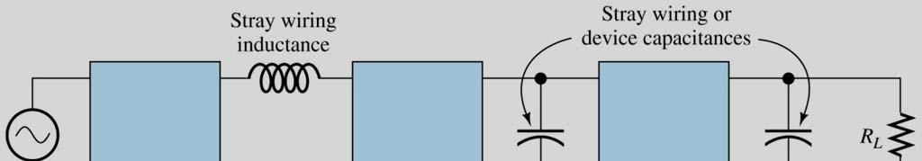
14 ac Couplng Slide 14
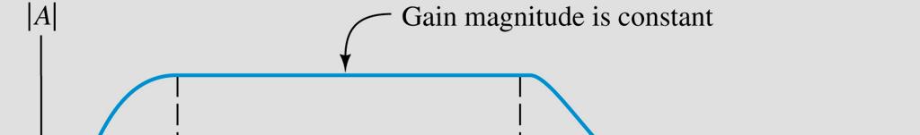
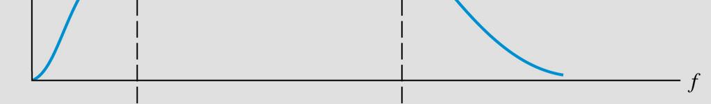
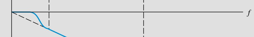
15 Pulse esponse: ise time, inging, and Tilt ise Time Slide 15
/f H Slide")
16 ise Time (estimate only) For f H =1/C, tr~ln(9)/f H Slide 16


17 inging (qualitatie only) Amplifier has a peaked response at f r 1/f r Slide 17

18 Tilt (estimate only) For f L ~1/C Slide 18
19 Linear Waeform Distortion Let the Phasor Amplifier Gain be H(ω)=A(ω)e j θ(ω) With in (t) = o cos[ωt+θ]= e{ o e j(ωt+θ) } out (t) = e{a(ω) o e j(ωt+θ+ θ(ω) } =A(ω) o cos[ωt+θ+ θ(ω)] Therefore, zero waeform distortion if A(ω) independent of ω and θ(ω)=0 or A(ω) independent of ω and θ(ω)=kω out (t) =A(ω) o cos[ω(t+k)+θ] - just a time shift Slide 19
20 Linear Waeform Distortion Amplitude Distortion A(ω) depends on ω Slide 20

")


21 Linear Waeform Distortion Phase Distortion θ(ω) depends on ω Example: (ω)=45 = o for all ω Slide 21
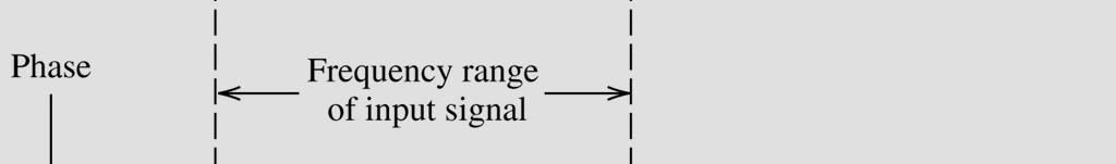

22 Conditions for zero Linear Waeform Distortion Slide 22
 Polynomial expansion")
 3 + = Vo+ V 1 cos(ωt)+ V 2 cos(2ωt)+")

23 Non-Linear Waeform Distortion Harmonic Distortion i =Kcos(ωt) Polynomial expansion of o =f( i ) o =A o +A 1 i +A 2 ( i ) 2 +A 3 ( i ) 3 + = Vo+ V 1 cos(ωt)+ V 2 cos(2ωt)+ Total Harmonic Distortion 2nd harmonic THD = 2 V 2 V V 3 4 V + 1 V + 1 V Slide 23
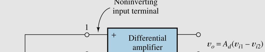


24 Differential Amplifier Slide 24

 + o = A d id Acm icm differential mode gain common mode")
25 Differential Signal and Common Mode Signal edefine the inputs in terms of two other oltages: 1. differential mode input id i1 i2 2. common mode input icm ( i1 + i2 )/2 so that i1 = icm + ( id /2) and i2 = icm - ( id /2) + o = A d id Acm icm differential mode gain common mode gain Slide 25
26 Common Mode ejection atio Example CM (in db) = 20log A d A cm Differential signal from sensor = 1mV (peak). We want outputs signal > 1V implies A d > 1000 Common mode signal =100V (from power line). We want common mode signal < 0.1V implies A cm <10-4 Therefore CM needs to be > 20log(10 7 )= 140dB Slide 26


27 A cm Measurement Measurement of CM A d Measurement Slide 27
28 Example: Differential Amplifier OpAmp Circuit b i + a + + i n + + a c i p + o + + p n b d a b b b a d o + = ) ( ) ( p = 0 + b o n a a n d a a b d c a o + ) ( i n = 0 ( ) b h If Slide 28 n b d c d p = + = i p = 0 ( ) a b a b o d c b a = = then, If
29 Differential Amplifier (cont d) If a b = CM= c d, then A cm = 0 and If the resistors are not perfectly matched, o 0 een when a = b. The common mode rejection ratio is finite: A d = b a CM A A d cm 1 + b ε / a if a b = (1 ε) c d *To get good common-mode mode rejection, you need well-matched resistors ( a and c, b and d ), such as 100kΩ 0.01% resistors Slide 29
30 Instrumentation Amplifier Sensor applications frequently requiring a differential amplifier with ery large input resistance for both the inerting and non inerting inputs. An instrumentation amplifier employs two non inerting amplifiers to buffer the input signal, followed by an inerting stage that forms the difference. Slide 30
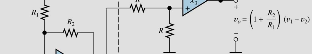
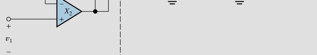
31 Instrumentation Amplifier CMM does not depend on internal resistances of 1 and 2 Slide 31


32 Offset Voltage, Offset Current, and Bias Current For direct coupled amplifiers, unbalanced internal components can cause a nonzero output een input sources are zero. Three current sources and one oltage sources are added to model this imperfection V off =offset oltage source I off =offset current source I B = Bias current Slide 32

+ A cm icm = 1000(0.001667+0.001667)+1(0.01)=3.")
33 Example Calculation Gien V off =2mV I B = 100nA I off = 20nA A cm =1 A d =100 Both input terminals to ground through 100kΩ resistors Use superposition Vo = A d (V off +V Ioff )+ A cm icm = 1000( )+1(0.01)=3.343V Slide 33
12/01/2009. Practice with past exams
 EE40 Final Exam Review Prof. Nathan Cheung 12/01/2009 Practice with past exams http://hkn.eecs.berkeley.edu/exam/list/?examcourse=ee%2040 Slide 1 Overview of Course Circuit components: R, C, L, sources
Chapter 11 Operational Amplifiers and Applications
 Chapter Operational Amplifiers and Applications Chapter Goals Understand the magic of negatie feedback and the characteristics of ideal op amps. Understand the conditions for non-ideal op amp behaior so
Chapter Goal. Zulfiqar Ali
 Chapter Goal Understand behaior and characteristics of ideal differential and op amps. Demonstrate circuit analysis techniques for ideal op amps. Characterize inerting, non-inerting, summing and instrumentation
CHAPTER 2 OPERATIONAL AMPLIFIERS
 CHPTE PETNL MPLFES Chapter utline. The deal p mp. The nerting Configuration. The Noninerting Configuration. Difference mplifiers.5 ntegrators and Differentiators.6 DC mperfections.7 Effect of Finite pen
55:041 Electronic Circuits
 55:04 Electronic Circuits Lecture -5 eiew of Op-Amps Sections of Chapters 9 & 4 A. Kruger Op-Amp eiew- eal-world Op-Amp In earlier courses, op-amp were often considered ideal Infinite input resistance
ES250: Electrical Science. HW6: The Operational Amplifier
 ES250: Electrical Science HW6: The Operational Amplifier Introduction This chapter introduces the operational amplifier or op amp We will learn how to analyze and design circuits that contain op amps,
Lecture 16: Small Signal Amplifiers
 Lecture 16: Small Signal Amplifiers Prof. Niknejad Lecture Outline Review: Small Signal Analysis Two Port Circuits Voltage Amplifiers Current Amplifiers Transconductance Amps Transresistance Amps Example:
Common mode rejection ratio
 Common mode rejection ratio Definition: Common mode rejection ratio represents the ratio of the differential voltage gaina d tothecommonmodevoltagegain,a cm : Common mode rejection ratio Definition: Common
Circuit produces an amplified negative version of v IN = R R R
 Inerting Amplifier Circuit produces an amplified negatie ersion of i = i, = 2 0 = 2 OUT OUT = 2 Example: Calculate OUT / and I for = 0.5V Solution: A V OUT 2 = = = 0 kω = 0 kω i 05. V = = = kω 05. ma
Applied Electronics II
 Applied Electronics II Chapter 3: Operational Amplifier Part 1- Op Amp Basics School of Electrical and Computer Engineering Addis Ababa Institute of Technology Addis Ababa University Daniel D./Getachew
Introduction to Operational Amplifiers
 P. R. Nelson ECE 322 Fall 2012 p. 1/50 Introduction to Operational Amplifiers Phyllis R. Nelson prnelson@csupomona.edu Professor, Department of Electrical and Computer Engineering California State Polytechnic
Chapter 2. Operational Amplifiers
 Chapter 2. Operational Amplifiers Tong In Oh 1 2.3 The Noninverting Configuration v I is applied directly to the positive input terminal of the op amp One terminal of is connected to ground Closed-loop
Course Outline. 4. Chapter 5: MOS Field Effect Transistors (MOSFET) 5. Chapter 6: Bipolar Junction Transistors (BJT)
 5. Chapter 6: Bipolar Junction Transistors (BJT)") Course Outline 1. Chapter 1: Signals and Amplifiers 1 2. Chapter 3: Semiconductors 3. Chapter 4: Diodes 4. Chapter 5: MOS Field Effect Transistors (MOSFET) 5. Chapter 6: Bipolar Junction Transistors (BJT)
Course Outline 1. Chapter 1: Signals and Amplifiers 1 2. Chapter 3: Semiconductors 3. Chapter 4: Diodes 4. Chapter 5: MOS Field Effect Transistors (MOSFET) 5. Chapter 6: Bipolar Junction Transistors (BJT)
ECE4902 C Lab 7
 ECE902 C2012 - Lab MOSFET Differential Amplifier Resistive Load Active Load PURPOSE: The primary purpose of this lab is to measure the performance of the differential amplifier. This is an important topology
Combination Notch and Bandpass Filter
 Combination Notch and Bandpass Filter Clever filter design for graphic equalizer can perform both notch and bandpass functions Gain or attenuation is controlled by a potentiometer for specific frequency
Chapter 15 Goals. ac-coupled Amplifiers Example of a Three-Stage Amplifier
 Chapter 15 Goals ac-coupled multistage amplifiers including voltage gain, input and output resistances, and small-signal limitations. dc-coupled multistage amplifiers. Darlington configuration and cascode
Differential Amplifier : input. resistance. Differential amplifiers are widely used in engineering instrumentation
 Differential Amplifier : input resistance Differential amplifiers are widely used in engineering instrumentation Differential Amplifier : input resistance v 2 v 1 ir 1 ir 1 2iR 1 R in v 2 i v 1 2R 1 Differential
EE4902 C Lab 7
 EE4902 C2007 - Lab 7 MOSFET Differential Amplifier Resistive Load Active Load PURPOSE: The primary purpose of this lab is to measure the performance of the differential amplifier. This is an important
4. Differential Amplifiers. Electronic Circuits. Prof. Dr. Qiuting Huang Integrated Systems Laboratory
 4. Differential Amplifiers Electronic Circuits Prof. Dr. Qiuting Huang Integrated Systems Laboratory Differential Signaling Basics and Motivation Transmitting information with two complementary signals
OPERATIONAL AMPLIFIER & VOLTAGE REFERENCE KL103/A TECHNICAL DATA DESCRIPTION. PIN CONNECTIONS (top view) OPERATIONAL AMPLIFIER
 OPERATIONAL AMPLIFIER") TECHNICAL DATA OPERATIONAL AMPLIFIER & OLTAGE REFERENCE KL13/A OPERATIONAL AMPLIFIER LOW INPUT OFFSET OLTAGE :. typ. LOW SUPPLY CURRENT : 3 A/op. (@ cc = ) MEDIUM BANDWIDTH (unity gain) :.9MHz LARGE OUTPUT
TECHNICAL DATA OPERATIONAL AMPLIFIER & OLTAGE REFERENCE KL13/A OPERATIONAL AMPLIFIER LOW INPUT OFFSET OLTAGE :. typ. LOW SUPPLY CURRENT : 3 A/op. (@ cc = ) MEDIUM BANDWIDTH (unity gain) :.9MHz LARGE OUTPUT
Lab Experiment #2 Differential Amplifiers. Group Members
 Lab Experiment #2 Differential Amplifiers Group Members Student 1 Student 2 Student 3 Student Name Surname First Name Student ID # Pre-Lab Mark (out of 30) Lab Demo and performance (out of 70) Total Lab
MOSFET Amplifier Configuration. MOSFET Amplifier Configuration
 MOSFET Amplifier Configuration Single stage The signal is fed to the amplifier represented as sig with an internal resistance sig. MOSFET is represented by its small signal model. Generally interested
Lecture 20 Transistor Amplifiers (II) Other Amplifier Stages. November 17, 2005
 Other Amplifier Stages. November 17, 2005") 6.012 Microelectronic Devices and Circuits Fall 2005 Lecture 20 1 Lecture 20 Transistor Amplifiers (II) Other Amplifier Stages November 17, 2005 Contents: 1. Common source amplifier (cont.) 2. Common drain
6.012 Microelectronic Devices and Circuits Fall 2005 Lecture 20 1 Lecture 20 Transistor Amplifiers (II) Other Amplifier Stages November 17, 2005 Contents: 1. Common source amplifier (cont.) 2. Common drain
ELECTRONIC DEVICES. Assist. prof. Laura-Nicoleta IVANCIU, Ph.D. C8 Summing and differential amplifiers with OpAmp
 ELECTNIC DEVICES Assist. prof. Laura-Nicoleta IVANCIU, Ph.D. C8 Summing and differential amplifiers with pamp C8 Summing and differential amplifs w/ pamp Contents Summing amplifiers with pamp Inerting
MOSFET Common Source Amplifier
 Microelectronic Circuits MOSFET Common Source Amplifier Slide 1 Small nal Model The definition of Transconductance g m i D S S S k n W L O The definition of output resistance r o DS I The definition of
Section 6 Chapter 2: Operational Amplifiers
 03 Section 6 Chapter : Operational Amplifiers eference : Microelectronic circuits Sedra sixth edition 4//03 4//03 Contents: - DC imperfections A. Offset voltage B. Solution of offset voltage C. Input bias
ECE:3410 Electronic Circuits
 ECE:3410 Electronic Circuits Reiew of Op-Amps Sections of Chapters 9 & 14 A. Kruger Op-Amp Reiew-1 Real-World Op-Amp In earlier courses, op-amp were often considered ideal Infinite input resistance Infinite
Chapter 6: Operational Amplifier (Op Amp)
") Chapter 6: Operational Amplifier (Op Amp) 6.1 What is an Op Amp? 6.2 Ideal Op Amp 6.3 Nodal Analysis of Circuits with Op Amps 6.4 Configurations of Op Amp 6.5 Cascaded Op Amp 6.6 Op Amp Circuits & Linear
Chapter 6: Operational Amplifier (Op Amp) 6.1 What is an Op Amp? 6.2 Ideal Op Amp 6.3 Nodal Analysis of Circuits with Op Amps 6.4 Configurations of Op Amp 6.5 Cascaded Op Amp 6.6 Op Amp Circuits & Linear
ECE 442 Solid State Devices & Circuits. 15. Differential Amplifiers
 ECE 442 Solid State Devices & Circuits 15. Differential Amplifiers Jose E. Schutt-Aine Electrical & Computer Engineering University of Illinois jschutt@emlab.uiuc.edu ECE 442 Jose Schutt Aine 1 Background
MC1458 MC1558 DUAL OPERATIONAL AMPLIFIERS.LOW POWER CONSUMPTION + - LARGE INPUT VOLTAGE RANGE NO LATCH-UP
 MC1458 MC1558 DUAL OPEATIONAL AMPLIFIES.LOW POWE CONSUMPTION LAGE INPUT OLTAGE ANGE NO LATCH-UP. HIGH GAIN SHOT-CICUIT POTECTION NO FEQUENCY COMPENSATION EQUIED DESCIPTION The MC1458 is a high performance
55:041 Electronic Circuits
 55:041 Electronic Circuits Reiew of Op-Amps Sections of Chapters 9 & 14 A. Kruger Op-Amp Reiew-1 Real-World Op-Amp In earlier courses, op-amp were often considered ideal Infinite input resistance Infinite
Lecture 2: Non-Ideal Amps and Op-Amps
 Lecture 2: Non-Ideal Amps and Op-Amps Prof. Ali M. Niknejad Department of EECS University of California, Berkeley Practical Op-Amps Linear Imperfections: Finite open-loop gain (A 0 < ) Finite input resistance
Reading. Lecture 33: Context. Lecture Outline. Chapter 9, multi-stage amplifiers. Prof. J. S. Smith
 eading Lecture 33: Chapter 9, multi-stage amplifiers Prof J. S. Smith Context Lecture Outline We are continuing to review some of the building blocks for multi-stage amplifiers, including current sources
Precision Rectifier Circuits
 Precision Rectifier Circuits Rectifier circuits are used in the design of power supply circuits. In such applications, the voltage being rectified are usually much greater than the diode voltage drop,
Unit 6 Operational Amplifiers Chapter 5 (Sedra and Smith)
") Unit 6 Operational Amplifiers Chapter 5 (Sedra and Smith) Prepared by: S V UMA, Associate Professor, Department of ECE, RNSIT, Bangalore Reference: Microelectronic Circuits Adel Sedra and K C Smith 1 Objectives
Unit 6 Operational Amplifiers Chapter 5 (Sedra and Smith) Prepared by: S V UMA, Associate Professor, Department of ECE, RNSIT, Bangalore Reference: Microelectronic Circuits Adel Sedra and K C Smith 1 Objectives
Q1. Explain the Astable Operation of multivibrator using 555 Timer IC.
 Q1. Explain the Astable Operation of multivibrator using 555 Timer I. Answer: The following figure shows the 555 Timer connected for astable operation. A V PIN 8 PIN 7 B 5K PIN6 - S Q 5K PIN2 - Q PIN3
Chapter 5. Operational Amplifiers and Source Followers. 5.1 Operational Amplifier
 Chapter 5 Operational Amplifiers and Source Followers 5.1 Operational Amplifier In single ended operation the output is measured with respect to a fixed potential, usually ground, whereas in double-ended
ELECTRONIC DEVICES. Assist. prof. Laura-Nicoleta IVANCIU, Ph.D. C9 Applications with OpAmp - 1
 ELECTONIC DEVICES Assist. prof. Laura-Nicoleta IVANCIU, Ph.D. C9 Applications with OpAmp - C9 Applications with OpAmp - Contents Voltage domain conersion circuits Capacitiely coupled amplifiers Op-amp
NJM2722. Single Ultra-High speed and Wide Band Operational Amplifier
 Single Ultra-High speed and Wide Band Operational Amplifier GENERAL DESCRIPTION The NJM2722 is a single, ultra-high speed and wide band operational amplifier that features 1V/μs slew rate and 1ohm load
Chapter 8. Chapter 9. Chapter 6. Chapter 10. Chapter 11. Chapter 7
 5.5 Series and Parallel Combinations of 246 Complex Impedances 5.6 Steady-State AC Node-Voltage 247 Analysis 5.7 AC Power Calculations 256 5.8 Using Power Triangles 258 5.9 Power-Factor Correction 261
Lecture 13 Date:
 Lecture 13 Date: 9.09.016 Common Mode Rejection Ratio NonIdealities in Differential mplifier Common Mode Rejection Ratio (CMRR) Differential input amplifiers are devices/circuits that can input and amplify
Objectives The purpose of this lab is build and analyze Differential amplifiers based on NMOS transistors (or NPN transistors).
.") 1 Lab 03: Differential Amplifiers (MOSFET) (20 points) NOTE: 1) Please use the basic current mirror from Lab01 for the second part of the lab (Fig. 3). 2) You can use the same chip as the basic current
1 Lab 03: Differential Amplifiers (MOSFET) (20 points) NOTE: 1) Please use the basic current mirror from Lab01 for the second part of the lab (Fig. 3). 2) You can use the same chip as the basic current
JFET Application Current Source
 MOSFET Op mps, 5 Imperfections Opamp applications Daylight sags cknowledgements: on oscoe, Neamen, Donald: Microelectronics Circuit nalysis and Design, rd Edition JFET pplication Current Source Household
Nonlinear Macromodeling of Amplifiers and Applications to Filter Design.
 ECEN 622(ESS) Nonlinear Macromodeling of Amplifiers and Applications to Filter Design. By Edgar Sanchez-Sinencio Thanks to Heng Zhang for part of the material OP AMP MACROMODELS Systems containing a significant
Introduction to Analog Interfacing. ECE/CS 5780/6780: Embedded System Design. Various Op Amps. Ideal Op Amps
 Introduction to Analog Interfacing ECE/CS 5780/6780: Embedded System Design Scott R. Little Lecture 19: Operational Amplifiers Most embedded systems include components that measure and/or control real-world
LF147 - LF247 LF347 WIDE BANDWIDTH QUAD J-FET OPERATIONAL AMPLIFIERS
 LF147 - LF247 LF347 WIDE BANDWIDTH QUAD J-FET OPERATIONAL AMPLIFIERS LOW POWER CONSUMPTION WIDE COMMON-MODE (UP TO V + CC ) AND DIFFERENTIAL VOLTAGE RANGE LOW INPUT BIAS AND OFFSET CURRENT OUTPUT SHORT-CIRCUIT
Operational Amplifiers. Boylestad Chapter 10
 Operational Amplifiers Boylestad Chapter 10 DC-Offset Parameters Even when the input voltage is zero, an op-amp can have an output offset. The following can cause this offset: Input offset voltage Input
Mixer. General Considerations V RF VLO. Noise. nonlinear, R ON
 007/Nov/7 Mixer General Considerations LO S M F F LO L Noise ( a) nonlinearity (b) Figure 6.5 (a) Simple switch used as mixer (b) implementation of switch with an NMOS device. espect to espect to It is
Analog Circuits. Operational Amplifiers (Opamps) DC Power Supplies Oscillators
 DC Power Supplies Oscillators") Analog Circuits Operational Amplifiers (Opamps) DC Power Supplies Oscillators Operational Amplifiers Highgain differential amplifier, using voltage feedback, providing stabilized voltage gain Symbol of
Analog Circuits Operational Amplifiers (Opamps) DC Power Supplies Oscillators Operational Amplifiers Highgain differential amplifier, using voltage feedback, providing stabilized voltage gain Symbol of
Gechstudentszone.wordpress.com
 UNIT 4: Small Signal Analysis of Amplifiers 4.1 Basic FET Amplifiers In the last chapter, we described the operation of the FET, in particular the MOSFET, and analyzed and designed the dc response of circuits
Introduction to Op Amps
 Introduction to Op Amps ENGI 242 ELEC 222 Basic Op-Amp The op-amp is a differential amplifier with a very high open loop gain 25k AVOL 500k (much higher for FET inputs) high input impedance 500kΩ ZIN 10MΩ
BJT Amplifier. Superposition principle (linear amplifier)
") BJT Amplifier Two types analysis DC analysis Applied DC voltage source AC analysis Time varying signal source Superposition principle (linear amplifier) The response of a linear amplifier circuit excited
BJT Amplifier Two types analysis DC analysis Applied DC voltage source AC analysis Time varying signal source Superposition principle (linear amplifier) The response of a linear amplifier circuit excited
The Miller Approximation. CE Frequency Response. The exact analysis is worked out on pp of H&S.
 CE Frequency Response The exact analysis is worked out on pp. 639-64 of H&S. The Miller Approximation Therefore, we consider the effect of C µ on the input node only V ---------- out V s = r g π m ------------------
UNIT - 1 OPERATIONAL AMPLIFIER FUNDAMENTALS
 UNIT - 1 OPERATIONAL AMPLIFIER FUNDAMENTALS 1.1 Basic operational amplifier circuit- hte basic circuit of an operational amplifier is as shown in above fig. has a differential amplifier input stage and
CHAPTER 8 DIFFERENTIAL AND MULTISTAGE AMPLIFIERS
 CHAPTER 8 DIFFERENTIAL AND MULTISTAGE AMPLIFIERS Chapter Outline 8.1 The CMOS Differential Pair 8. Small-Signal Operations of the MOS Differential Pair 8.3 The BJT Differential Pair 8.4 Other Non-ideal
Homework Assignment True or false. For both the inverting and noninverting op-amp configurations, V OS results in
 Question 1 (Short Takes), 2 points each. Homework Assignment 02 1. An op-amp has input bias current I B = 1 μa. Make an estimate for the input offset current I OS. Answer. I OS is normally an order of
TL072 TL072A - TL072B
 A - B LOW NOISE J-FET DUAL OPERATIONAL AMPLIFIERS WIDE COMMON-MODE (UP TO V + CC ) AND DIFFERENTIAL VOLTAGE RANGE LOW INPUT BIAS AND OFFSET CURRENT LOW NOISE e n = 15nV/ Hz (typ) OUTPUT SHORT-CIRCUIT PROTECTION
Chapter 10: Operational Amplifiers
 Chapter 10: Operational Amplifiers Differential Amplifier Differential amplifier has two identical transistors with two inputs and two outputs. 2 Differential Amplifier Differential amplifier has two identical
Lecture Notes Unit-III
 Lecture Notes Unit-III FAQs Q1: An operational amplifier has a differential gain of 103 and CMRR of 100, input voltages are 120µV and 80µV, determine output voltage. 2 MARKS
Dual, Ultralow Distortion, Ultralow Noise Op Amp AD8599
 Dual, Ultralow Distortion, Ultralow Noise Op Amp FEATURES Low noise: 1 nv/ Hz at 1 khz Low distortion: 5 db THD @ khz
LF153 LF253 - LF353 WIDE BANDWIDTH DUAL J-FET OPERATIONAL AMPLIFIERS
 LF153 LF253 - LF353 WIDE BANDWIDTH DUAL J-FET OPERATIONAL AMPLIFIERS LOW POWER CONSUMPTION WIDE COMMON-MODE (UP TO V + CC ) AND DIFFERENTIAL VOLTAGE RANGE LOW INPUT BIAS AND OFFSET CURRENT OUTPUT SHORT-CIRCUIT
UNISONIC TECHNOLOGIES CO., LTD KA8602
 UNISONIC TECHNOLOGIES CO., LTD KA02 LOW VOLTAGE AUDIO POWER AMPLIFIER DESCRIPTION The UTC KA02 is the audio power amplifier available for low voltage. The UTC KA02 supplies differential outputs for maximizing
Objectives The purpose of this lab is build and analyze Differential amplifier based on NPN transistors.
 1 Lab 03: Differential Amplifier Total 30 points: 20 points for lab, 5 points for well-organized report, 5 points for immaculate circuit on breadboard NOTES: 1) Please use the basic current mirror from
Operational Amplifier as A Black Box
 Chapter 8 Operational Amplifier as A Black Box 8. General Considerations 8.2 Op-Amp-Based Circuits 8.3 Nonlinear Functions 8.4 Op-Amp Nonidealities 8.5 Design Examples Chapter Outline CH8 Operational Amplifier
ECE-342 Test 1: Sep 27, :00-8:00, Closed Book. Name : SOLUTION
 ECE-342 Test 1: Sep 27, 2011 6:00-8:00, Closed Book Name : SOLUTION All solutions must provide units as appropriate. Use the physical constants and data as provided on the formula sheet the last page of
Instrumentation Amplifiers Filters Integrators Differentiators Frequency-Gain Relation Non-Linear Op-Amp Applications DC Imperfections
 Lecture Op-Amp Building Blocks and Applications Instrumentation Amplifiers Filters Integrators Differentiators Frequency-Gain elation Non-Linear Op-Amp Applications DC Imperfections ELG439 Check List for
Electronics basics for MEMS and Microsensors course
 Electronics basics for course, a.a. 2017/2018, M.Sc. in Electronics Engineering Transfer function 2 X(s) T(s) Y(s) T S = Y s X(s) The transfer function of a linear time-invariant (LTI) system is the function
General Purpose Operational Amplifiers
 General Purpose Operational Amplifiers OUTLINE Lecture 0, 0/7/05 Corrected 0/9/05 Op-Amp from -Port Blocks Op-Amp Model and its Idealization Negative Feedback for Stability Components around Op-Amp define
Week 7: Common-Collector Amplifier, MOS Field Effect Transistor
 EE 2110A Electronic Circuits Week 7: Common-Collector Amplifier, MOS Field Effect Transistor ecture 07-1 Topics to coer Common-Collector Amplifier MOS Field Effect Transistor Physical Operation and I-V
NJM2737. Low Noise, Rail-to-Rail Input/Output Dual Operational Amplifier
 Low Noise, Rail-to-Rail Input/Output Dual Operational Amplifier GENERAL DESCRIPTION The NJM2737 is a Rail-to-Rail Input/Output single supply dual operational amplifier featuring low voltage operation,
6.976 High Speed Communication Circuits and Systems Lecture 8 Noise Figure, Impact of Amplifier Nonlinearities
 6.976 High Speed Communication Circuits and Systems Lecture 8 Noise Figure, Impact of Amplifier Nonlinearities Michael Perrott Massachusetts Institute of Technology Copyright 2003 by Michael H. Perrott
Analog Integrated Circuit Design Exercise 1
 Analog Integrated Circuit Design Exercise 1 Integrated Electronic Systems Lab Prof. Dr.-Ing. Klaus Hofmann M.Sc. Katrin Hirmer, M.Sc. Sreekesh Lakshminarayanan Status: 21.10.2015 Pre-Assignments The lecture
444 Index. F Fermi potential, 146 FGMOS transistor, 20 23, 57, 83, 84, 98, 205, 208, 213, 215, 216, 241, 242, 251, 280, 311, 318, 332, 354, 407
 Index A Accuracy active resistor structures, 46, 323, 328, 329, 341, 344, 360 computational circuits, 171 differential amplifiers, 30, 31 exponential circuits, 285, 291, 292 multifunctional structures,
EE105 Fall 2015 Microelectronic Devices and Circuits Multi-Stage Amplifiers. Prof. Ming C. Wu 511 Sutardja Dai Hall (SDH)
") EE105 Fall 2015 Microelectronic Devices and Circuits Multi-Stage Amplifiers Prof. Ming C. Wu wu@eecs.berkeley.edu 511 Sutardja Dai Hall (SDH) Differential & Common Mode Signals Why Differential? Differential
EE105 Fall 2015 Microelectronic Devices and Circuits Multi-Stage Amplifiers Prof. Ming C. Wu wu@eecs.berkeley.edu 511 Sutardja Dai Hall (SDH) Differential & Common Mode Signals Why Differential? Differential
Nonlinear Macromodeling of Amplifiers and Applications to Filter Design.
 ECEN 622 Nonlinear Macromodeling of Amplifiers and Applications to Filter Design. By Edgar Sanchez-Sinencio Thanks to Heng Zhang for part of the material OP AMP MACROMODELS Systems containing a significant
The Differential Amplifier. BJT Differential Pair
 1 The Differential Amplifier Asst. Prof. MONTREE SRPRUCHYANUN, D. Eng. Dept. of Teacher Training in Electrical Engineering, Faculty of Technical Education King Mongkut s nstitute of Technology North Bangkok
HOME ASSIGNMENT. Figure.Q3
 HOME ASSIGNMENT 1. For the differential amplifier circuit shown below in figure.q1, let I=1 ma, V CC =5V, v CM = -2V, R C =3kΩ and β=100. Assume that the BJTs have v BE =0.7 V at i C =1 ma. Find the voltage
QUESTION BANK for Analog Electronics 4EC111 *
 OpenStax-CNX module: m54983 1 QUESTION BANK for Analog Electronics 4EC111 * Bijay_Kumar Sharma This work is produced by OpenStax-CNX and licensed under the Creative Commons Attribution License 4.0 Abstract
ECEN 325 Lab 5: Operational Amplifiers Part III
 ECEN Lab : Operational Amplifiers Part III Objectives The purpose of the lab is to study some of the opamp configurations commonly found in practical applications and also investigate the non-idealities
EEE118: Electronic Devices and Circuits
 EEE118: Electronic Devices and Circuits Lecture XIV James E Green Department of Electronic Engineering University of Sheffield j.e.green@sheffield.ac.uk Review Review Considered several transistor switching
High Common-Mode Rejection. Differential Line Receiver SSM2141 REV. B FUNCTIONAL BLOCK DIAGRAM FEATURES. High Common-Mode Rejection
 a FEATURES High Common-Mode Rejection DC: 100 db typ 60 Hz: 100 db typ 20 khz: 70 db typ 40 khz: 62 db typ Low Distortion: 0.001% typ Fast Slew Rate: 9.5 V/ s typ Wide Bandwidth: 3 MHz typ Low Cost Complements
Chapter 14 Operational Amplifiers
 1. List the characteristics of ideal op amps. 2. Identify negative feedback in op-amp circuits. 3. Analyze ideal op-amp circuits that have negative feedback using the summing-point constraint. ELECTRICAL
NJM2720. Single Ultra-High speed and Wide Band Operational Amplifier
 NJM272 Single Ultra-High speed and Wide Band Operational Amplifier GENERAL DESCRIPTION The NJM272 is a single, ultra-high speed and wide band operational amplifier that features 2V/μs slew rate and 1ohm
SAMPLE FINAL EXAMINATION FALL TERM
 ENGINEERING SCIENCES 154 ELECTRONIC DEVICES AND CIRCUITS SAMPLE FINAL EXAMINATION FALL TERM 2001-2002 NAME Some Possible Solutions a. Please answer all of the questions in the spaces provided. If you need
EE105 Fall 2015 Microelectronic Devices and Circuits
 EE105 Fall 2015 Microelectronic Devices and Circuits Multi-Stage Amplifiers Prof. Ming C. Wu wu@eecs.berkeley.edu 511 Sutardja Dai Hall (SDH) Terminal Gain and I/O Resistances of MOS Amplifiers Common
Homework Assignment 03
 Homework Assignment 03 Question 1 (Short Takes), 2 points each unless otherwise noted. 1. Two 0.68 μf capacitors are connected in series across a 10 khz sine wave signal source. The total capacitive reactance
Chapter 8 Differential and Multistage Amplifiers
 1 Chapter 8 Differential and Multistage Amplifiers Operational Amplifier Circuit Components 2 1. Ch 7: Current Mirrors and Biasing 2. Ch 9: Frequency Response 3. Ch 8: Active-Loaded Differential Pair 4.
UNISONIC TECHNOLOGIES CO., LTD TDA2050
 UNISONIC TECHNOLOGIES CO., LTD TDA2050 32W HI-FI AUDIO POWER AMPLIFIER DESCRIPTION The UTC TDA2050 is a monolithic integrated circuit with high power capability and is designed to use as an class AB audio
Lecture 19 - Transistor Amplifiers (I) Common-Source Amplifier. April 24, 2001
 Common-Source Amplifier. April 24, 2001") 6.012 Microelectronic Devices and Circuits Spring 2001 Lecture 191 Lecture 19 Transistor Amplifiers (I) CommonSource Amplifier April 24, 2001 Contents: 1. Amplifier fundamentals 2. Commonsource amplifier
6.012 Microelectronic Devices and Circuits Spring 2001 Lecture 191 Lecture 19 Transistor Amplifiers (I) CommonSource Amplifier April 24, 2001 Contents: 1. Amplifier fundamentals 2. Commonsource amplifier
F9 Differential and Multistage Amplifiers
 Lars Ohlsson 018-10-0 F9 Differential and Multistage Amplifiers Outline MOS differential pair Common mode signal operation Differential mode signal operation Large signal operation Small signal operation
Single Supply, Rail to Rail Low Power FET-Input Op Amp AD820
 a FEATURES True Single Supply Operation Output Swings Rail-to-Rail Input Voltage Range Extends Below Ground Single Supply Capability from + V to + V Dual Supply Capability from. V to 8 V Excellent Load
Lecture 33: Context. Prof. J. S. Smith
 Lecture 33: Prof J. S. Smith Context We are continuing to review some of the building blocks for multi-stage amplifiers, including current sources and cascode connected devices, and we will also look at
DUAL OP AMP AND VOLTAGE REFERENCE General Description. Features
 General Description The is a monolithic IC specifically designed to regulate the output current and voltage levels of switching battery chargers and power supplies. The device contains two Op Amps and
EE 230 Lecture 19. Nonideal Op Amp Characteristics. Offset Voltage Common-mode input range Compensation
 EE 230 Lecture 19 Nonideal Op Amp Characteristics Offset Voltage Common-mode input range Compensation Quiz 13 The operational amplifier has a GB of 20MHz. Determine the 3dB bandwidth of the closed-loop
Multistage Amplifiers
 Multistage Amplifiers Single-stage transistor amplifiers are inadequate for meeting most design requirements for any of the four amplifier types (voltage, current, transconductance, and transresistance.)
Chapter 10 Differential Amplifiers
 Chapter 10 Differential Amplifiers 10.1 General Considerations 10.2 Bipolar Differential Pair 10.3 MOS Differential Pair 10.4 Cascode Differential Amplifiers 10.5 Common-Mode Rejection 10.6 Differential
UNIT I. Operational Amplifiers
 UNIT I Operational Amplifiers Operational Amplifier: The operational amplifier is a direct-coupled high gain amplifier. It is a versatile multi-terminal device that can be used to amplify dc as well as
NJM2734SCC. Rail-to-Rail Input/Output Quad Operational Amplifier PACKAGE OUTLINE
 Rail-to-Rail Input/Output Quad Operational Amplifier GENERAL DESCRIPTION NJM74SCC is a Rail-to-Rail Input/Output quad operational amplifier featuring Low power, low noise and operation from.8v. Rail-to-Rail
OPERATIONAL AMPLIFIER PREPARED BY, PROF. CHIRAG H. RAVAL ASSISTANT PROFESSOR NIRMA UNIVRSITY
 OPERATIONAL AMPLIFIER PREPARED BY, PROF. CHIRAG H. RAVAL ASSISTANT PROFESSOR NIRMA UNIVRSITY INTRODUCTION Op-Amp means Operational Amplifier. Operational stands for mathematical operation like addition,
LF147 - LF247 LF347 WIDE BANDWIDTH QUAD J-FET OPERATIONAL AMPLIFIERS
 LF147 - LF247 LF347 WIDE BANDWIDTH QUAD J-FET OPERATIONAL AMPLIFIERS LOW POWER CONSUMPTION WIDE COMMON-MODE (UP TO V + CC ) AND DIFFERENTIAL VOLTAGE RANGE LOW INPUT BIAS AND OFFSET CURRENT OUTPUT SHORT-CIRCUIT