Series compensation of distribution and subtransmission lines
|
|
|
- Amberlynn Barker
- 6 years ago
- Views:
Transcription
1 University f Wllngng Research Online University f Wllngng Thesis Cllectin University f Wllngng Thesis Cllectins 1997 Series cmpensatin f distributin and subtransmissin lines Rbert Arthur Barr University f Wllngng Recmmended Citatin Barr, Rbert Arthur, Series cmpensatin f distributin and subtransmissin lines, Dctr f Philsphy thesis, Department f Electrical and Cmputer Engineering, University f Wllngng, Research Online is the pen access institutinal repsitry fr the University f Wllngng. Fr further infrmatin cntact Manager Repsitry Services: mrgan@uw.edu.au.
2
3 SERIES COMPENSATION OF DISTRIBUTION AND SUBTRANSMISSION LINES A thesis submitted in fulfilment f the requirements fr the award f the degree f DOCTOR OF PHILOSOPHY frm THE UNIVERSITY OF WOLLONGONG by Rbert Barr, B.E.(Hns),M.E.,C.P.Eng.,F.I.E.(Aust) Department f Electrical and Cmputer Engineering 1997
4 1 Dedicatin T my wife, Linda and children, Jane, Adrian and Karen. Acknwledgement I wish t express my appreciatin and gratitude t my supervisr, Dr Dn Piatt fr his mst valuable assistance with this prject. Declaratin I hereby certify that this thesis is entirely my wn wrk and has nt been submi the award f a degree t any ther university r institutin. RberBarr Series Cmpensatin f Distributin and Subtransmissin Lines
5 2 Abstract Series capacitrs can increase the pwer carrying capacity f subtransmissin and distributin lines by reducing vltage regulatin. When cnsidering series capacit cmpensatin f distributin lines and subtransmissin lines careful cnsideratin t be given t capacitr lcatin, ferrresnance, hmic reactive value, transient behaviur, shrt circuit withstand and capacitr prtectin. Cnventinal design appraches include shunt cnnected resistrs, spark gaps, metal xide varisters, thy cntrlled reactrs and bypass switches. This thesis describes the use f a saturating chke and damping resistr t cntrl ferrresnance, transients, and thrugh fault currents. A small scale labratry nn linear single phase ferrresnant circuit was cnstructed with realistic per unit cmpnent values. Bth 3rd and 2nd subharmnic ferrresnance mdes were predicted by mdelling and generated in practice. Chke and damping resistr parameters were selected by mdelling t eliminate all t unwanted ferrresnant states. Experimental wrk cnfirmed that all the unwanted ferrresnant states were eliminated frm the labratry circuit. The transient and circuit perfrmance f the system is cnsidered. The prpsed arrangement ffers an effective cuntermeasure t ferrresnance fr series cmpensated distributin line The system als allws sme cntrl f system fault levels and transient circuit behaviur. The technique is simple, effective and requires n sphisticated cntrl, prtectin r bypass switch systems. Series Cmpensatin f Distributin and Subtransmissin Lines
6 Table f Cntents /. Intrductin 2. Cmpensatin Effects n Line Vltage Ptfiles 3. An Overview f the Ferrresnance Phenmenn 4. Time Dmain Transient Ferrresnance Mdel 5. Frequency Dmain Ferrresnance Mdel 6. Labratry Ferrresnant Circuit "A" 7. Labratry Ferrresnant Circuit "B" 8. Stability f Frequency Dmain Ferrresnant Slutins_ 9. Management f Ferrresnance and Shrt Circuit Withstand 10. Existing Techniques fr Managing Ferrresnance and Shrt Circuit Curr 11. A New Technique fr Managing Ferrresnance Selectin Of Cmpnent Values Scaling Up T Real Distributin Netwrks Future Research Directins Cnclusins References 113 Series Cmpensatin f Distributin and Subtransmissin Lines
7 4 List f Appendices Appendix A Detailed Experimental and Frequency Dmain Mdel Results fr Circuit "A" 128 Appendix B Mdelled Transient RLC Behaviur fr Circuit "A" 131 Appendix C Detailed Experimental and Frequency Dmain Mdel Results fr Circuit "B" 134 Appendix D Mdelled Transient RLC Behaviur fr Circuit "B" 137 Appendix E Experimental Circuit "D" 3 Phase 140 Appendix F Mdelled stred Energy in Circuit "A" 142 Series Cmpensatin f Distributin and Subtransmissin Lines
8 5 List f Main Symbls c pwer frequency - radians per secnd X transfrmerfluxlinkage - weber turns X c chke flux linkage - weber turns e a mismatch vltage errr sine switch n angle - radians < ) V-I phase angle - radians fr frequency rati I distributin line current - amps L c i Chke leakage inductance - henrys R distributin line resistance - hms T pwer frequency perid - secnds Vc capacitr vltage - vlts Vd line vltage drp - vlts VI lad vltage - vlts Vs supply vltage - vlts X distributin line reactance - hms Xc capacitr reactance - hms Series Cmpensatin f Distributin and Subtransmissin Lines
9 6 1. Intrductin Series Cmpensatin in Pwer Distributin Systems Capacitrs have been used fr the series cmpensatin f transmissin and distributin lines fr many years. Series capacitr installatins have been described in the literature as far back as Pineer pwer system engineers were seriusly examining the merits and demerits f series capacitrs and analysing the subharmnic ferrresnance phenmena [401] in the 1930's Series capacitrs are nw in cmmn use at the transmissin level with hundreds f units in service thrughut the wrld. Althugh series capacitrs have been in use fr a lng time they have nt fund widespread acceptance as a viable ecnmic pwer system cmpnent at the distributin level. It is the use f series capacitrs at the distributin level that is the subject f this thesis Distributin pwer systems have special characteristics that make them different frm transmissin systems. This thesis is aimed at examining ways in which the viability and effectiveness f series capacitr cmpensatin can be imprved at the distributin level. The Series Capacitr Cmpensatin Circuit Figure 1 shws the typical vltage prfile f a very weak distributin lin a lumped lad at the end. The line resistance and reactance is distributed alng the line. As the lad varies frm light lad t full lad there is a substantial vltage difference seen by custmers. It is the difference between light lad and full lad vltage that in many cases limits the capacity f the line. Series Cmpensatin f Distributin and Subtransmissin Lines
10 AAAA^ -rrrnr^ Distributed line R & L 73 d 75 d O Figure 1 Vltage Prfile f a Weak Distributin Line Figure 2 shws the effect f series capacitr cmpensatin n the same li The pwer line supplying the transfrmer is represented by distributed linear inductance and resistance. The circuit cntains a series capacitr t tune ut the effects f the line inductance. When used fr series cmpensatin, the capacitance will nrmally be chsen s as t tune ut all r mst f the line inductance at the pwer frequency. ryma 7 ^ CAP, Distributed line R & L -yvvvxa-^nnp^ -a a.. CK 73 a Light Lad ±0.90 Figure 2 Vltage Prfile f a Weak Distributin Line with Series Capacitr Cmpensatin Series Cmpensatin f Distributin and Subtransmissin Lines
11 The fundamental issues cncerning series capacitrs are the same tday as they were in the pineering days f 1930's. Series capacitrs ffer the ptential t tune ut all r part f the series inductance f lines at the pwer frequency. This can result in reduced vltage regulatin, enhanced pwer transfer capability and imprved system stability. Series capacitrs are particularly attractive in cntrlling vltage fluctuatins assciated rapidly varying lads. With such significant ptential fr enhanced with pwer transfer capability the questin arises as t why series capacitrs have nt fund widespread use and acceptance at the distributin level Series capacitrs are nt in widespread use at the distributin level because the generatin f ferrresnant vervltages, fault level prblems, prblems assciated with capacitr withstand f heavy thrugh fault currents and high cst Series capacitrs can prduce subharmnic ferrresnant vervltages and currents. This phenmenn is generally nt well understd by pwer system engineers with the result that a series capacitr installatin is cnsidered a high risk ptin r simply nt cnsidered at all. The pssibility f serius damage t capacitrs, transfrmers and custmer installatins by ferrresnance is f real cncern and requires careful management. The experimental and mdelling wrk perfrmed in the curse f this prject has highlighted hw destructive ferrresnance can be Effective slutins t the prblems f ferrresnance and capacitr prtectin are f great ptential benefit. Analysis f mst large pwer system distributin netwrks will identify lcatins f high vltage regulatin where vltage cnditins culd be imprved by series cmpensatin. Series Cmpensatin f Distributin and Subtransmissin Lines
12 This thesis is cncerned with gaining a fundamental understanding f ferrresnance and ther series capacitr related prblems and develping new slutins. Imprved Vltage Cntrl with Series Capacitrs Vltage cntrl in electric pwer systems is f fundamental imprtance in achieving desired pwer flws and maintaining vltage levels within specified limits Great engineering effrt and capital expenditure is invested in pwer syste t prvide sufficient "system strength" t maintain vltage levels within the required margins. Distributin lines are nrmally limited in their lad carrying capacity by either thermal current rating cnsideratins r excessive vltage drp. In general terms distributin systems supplying high lad density areas such as Cmmercial Business Districts and areas f high density husing develpment tend t be current rating limited. Regins f lw lad density such as rural areas and reginal twns tend t be supplied by distributin systems that are vltage drp limited High vltage regulatin in distributin feeders is nt the main limitatin itself. It is the vltage variatin between light lad and full lad that limits the maximum feeder lads that can be accmmdated. With ff circuit transfrmer taps n distributin transfrmers, the vltage variatin in the high vltage distributin feeder is directly reflected n t lw vltage custmers. Australian Standard AS2926 sets maximum vltage variatin at +6% t -6% r 226V t 254V in a 240V system There are many engineering appraches t vercming prblems f excessive vltage regulatin including augmentatin f lines, cnstructin f additinal lines, shunt capacitrs, vltage regulatrs (n lad tap changing aut transfrmers), n lad tap changing transfrmers and cnstructin f new Series Cmpensatin f Distributin and Subtransmissin Lines
13 10 substatins. These appraches ften invlve large capital csts in areas where there are lw lad densities. Develpment f a lw cst series cmpensatin arrangement fr distributin systems culd prvide significant advantages in selected situatins..4 Imprved System Stability with Series Capacitrs Series capacitrs can increase the stability f pwer systems by reducing th effective impedance f lines. Reduced line impedance has the effect f increasing system fault levels and increasing the strength f intercnnectin f a distributed netwrk f generatrs [512] [513],.5 Ferrresnance Ferrresnance is a well dcumented hazard f series capacitrs in distributin netwrks 102[103]. Ferrresnance can result in severe vervltages in capacitrs, distributin transfrmers and custmer installatins..6 Subsynchrnus Resnance Subsynchrnus resnance is a ptential hazard with series capacitrs [510], Subsynchrnus resnance invlves a lw frequency exchange f energy between a series capacitr and a generatr. Subsynchrnus resnance can cause the mechanical failure f generatr shafts..7 Asynchnus Resnance Asynchrnus resnance is a anther ptential prblem whereby mtrs can lck nt subharmnic frequencies n starting and cnsume abnrmally high currents [102]. Series Cmpensatin f Distributin and Subtransmissin Lines
14 11 2. Cmpensatin Effects n Line Vltage Prfiles 2.1 Uncmpensated Line Vltage Prfiles Figure 3 shws a phasr diagram fr the typical uncmpensated system with the crrespnding vltage prfile. IR sin(0) + IX cs(0) VI Figure 3 Phasr Diagram f an Uncmpensated Line The vltage drp Vd is defined by equatin (1) as the difference in magn between the supply vltage Vs and the lad vltage VI. As shwn n the phasr diagram, equatin (2) is a very gd apprximatin fr the vltage drp in shrt lines where transmissin line effects can be ignred. Equatin (2) Series Cmpensatin f Distributin and Subtransmissin Lines
15 12 remains a gd apprximatin fr mst distributin lines because the angle between Vs and VI is generally small. Vd= Vs - V1 (1) Vd «IRcs(< >) + IXsin(< >) (2) Equatin (2) describes the fundamentals f vltage drp perfrmance n distributin lines and is very useful fr analysing the varius frms f pwer system cmpensatin At n lad the lad current I will be zer and hence bth terms IR cs((j>) an IX sin((p) in equatin (2) will be zer. Under these cnditins there will be n line vltage drp. At full lad the vltage drp needs t be kept dwn t a manageable level (typically 5% t 15% f the supply vltage Vs). The aim is t minimise the line vltage drp, Vd. The line resistance, R, is determined by the line length and cnductr size and hence is a fundamental characteristic f the line. The parameters ver which cntrl is pssible are the effective inductive reactance f the line, X, and the effective lad pwer factr (i.e. X and cs(< >) ). The effective inductive reactance f the line, X, can be cntrlled by series capacitr cmpensatin and the effective lad pwer factr can be cntrlled by shunt capacitr cmpensatin. 2.2 Series Cmpensatin Line Vltage Prfiles With series cmpensatin the series capacitrs prduce a reactive impedance that typically cancels ut all r part f the line reactance, X. Under full cmpensatin cnditins the effective line reactance is zer and hence the term IX sin(<j>) frm equatin (2) becmes zer. The vltage drp n the line Series Cmpensatin f Distributin and Subtransmissin Lines
16 13 is nw a functin f the line resistance, lad current and lad pwer factr via the term IR cs(<j>) as shwn in equatin (3). Vdw IRcs((j>) (3) 2 Series capacitrs are mst effective in lines with a high X/R rati. If the X/R rati is less than unity then series capacitrs will tend t be ineffective. Lad pwer factr is als a cnsideratin with little r n benefit being gained if the pwer factr is clse t unity. 3 Figure 4 shws a typical vltage prfile f a fully series cmpensated line where the capacitr is lcated at the centre f the line. This figure clearly shws hw the installatin series capacitrs can significantly imprve the vltage variatins between full lad and light lad. IR sin<0) I Vc Vs CAP, Distributed line R 8. L VI Light Lad Figure 4 Phasr Diagram f a Fully Cmpensated Line Series Cmpensatin f Distributin and Subtransmissin Lines
17 Series capacitrs are nt a slutin t all line vltage drp prblems, hwever in the apprpriate lcatins they ffer the prspect f slving vltage and ther system prblems in a very effective manner. The key requirements fr a successful series cmpensatin scheme is a high X/R rati (say X/R>=1) and a pwer factr belw unity (say cs(< >)<=0.9). 2.3 Shunt Capacitr Cmpensatin Line Vltage Prfiles Shunt capacitr cmpensatin r pwer factr crrectin is the mst cmmn frm f cmpensatin used in pwer systems. Large industrial custmers are cmmnly required by electricity supply authrities t maintain their pwer factr abve a specified minimum. Pwer factr cntrl is ften achieved in these cases with shunt cnnected pwer factr crrectin capacitrs. Electricity supply authrities als use shunt cnnected capacitrs in critical parts f their netwrks t cntrl reactive pwer flws With shunt cmpensatin the line impedance remains unchanged. The shunt capacitrs increase the effective lad pwer factr twards unity by generating reactive pwer fr the lad. With reference t equatin (1) this means that the effective pwer factr cs(< )) mves twards unity and sin(( >) is driven tward zer. Under cnditins f full cmpensatin the term IX sin((j)) is driven t zer leaving the vltage drp as apprximately IR cs(<l)) The effectiveness f shunt cmpensatin is nt limited by the line inductive reactance. The ultimate limitatin in a shunt cmpensatin scheme is the line resistance. In practical shunt cmpensatin schemes the pwer factr may be lifted frm say 0.75 lagging (fr an industrial plant) up t 0.9. It wuld be rare and generally unecnmic t prvide sufficient cmpensatin t bring the pwer up int the range 0.95 t 1.0. Series Cmpensatin f Distributin and Subtransmissin Lines
18 Figure 5 shws a typical vltage prfile f a shunt capacitr cmpensatin scheme. The pssible vltageriseeffect is shwn if the capacitrs are left in service under light r n lad cnditins. T vercme this prblem capacitrs must be switched in and ut f service depending n the reactive lad requirements. This means that vltage changes ccur in discrete steps and switchgear and cntrl equipment is required. Unless specialised thyristr equipment is used it nt pssible t react t rapidly fluctuating lads. & i.. cs -p r uu Lad capacit rs in service serv'\ce _P 1.1 Light Lad capacitrs ut f service d0.8 Figure 5 Vltage Prfile Illustrating Shunt Capacitr Cmpensatin Harmnic resnances generated by variable speed drives and ther nn linear lads are becming an increasing prblem with shunt capacitrs [513]. Shunt capacitrs present a lw impedance t high frequency harmnics that can result in abnrmally high and destructive capacitr currents. 2.4 Cmparisn f Series and Shunt Cmpensatin Bth series and shunt capacitr cmpensatin have their advantages and disadvantages. Bth schemes have their place in pwer systems. Belw is a summary f the advantages and disadvantages. Series Cmpensatin f Distributin and SubUansmissin Lines
19 16 Series Capacitr Cmpensatin Advantages Cmpensatin naturally regulates with changes in lad current. Lw risk f prblems frm lad generated harmnics. Reduced line currents. Disadvantages Ferrresnance. Fault level cntrl. Capacitr fault level withstand. Shunt Capacitr Cmpensatin Advantages N inherent ferrresnance risk. Capacitrs d nt carry line fault currents. Reduced line currents. Disadvantages Autmatic regulatin nly pssible with expensive cntrl gear. Switchgear and cntrl equipment generally required. Vltage and VAR changes in discrete steps. Inability t respnd t rapid lad fluctuatins. Risk f vercurrent damage frm lad generated harmnics. Series Cmpensatin f Distributin and Subtransmissin Lines
20 Limitatins f Series and Shunt Capacitr Cmpensatin Schemes Bth series and shunt capacitr cmpensatin can nly prvide benefits if the pwer lad pwer factr is significantly belw unity. Althugh series and shunt cmpensatin perate in different ways they bth reduce the vltage drp effect f the line inductive reactance. Lines with a high resistance tend t be beynd any real scpe fr imprvement with any frm f cmpensatin scheme Capacitr cmpensatin techniques are cncerned with imprving the electrical perfrmance f the distributin netwrk. They cannt create a strng system if the existing line is f high resistance. A high line resistance generally means that a majr system augmentatin is the nly real slutin t severe vltage drp prblems Cmpensatin schemes in the crrect lcatins can be highly effective in imprving pwer system perfrmance. If installed withut due cnsideratins t the fundamentals, they are likely t be ineffective. Series Cmpensatin f Distributin and Subtransmissin Lines
21 18 3. An Overview f the Ferrresnance Phenmenn 3.1 The Nature f Ferrresnance Nrmal linear circuit resnance is well understd and the cnditins required fr resnance are well defined. The mst cmmn resnances in linear electric circuits invlve series/parallel capacitrs and inductances. Resnance(s) ccur at specific and easily predictable values f frequency, inductance and capacitance In circuits cnsisting f linear resistive, capacitive and inductive elements with cnstant vltage pwer frequency surces nly ne steady state slutin will exist. In these cases the branch currents and nde vltages are single valued and are predicable using standard circuit thery techniques Ferrresnance by cmparisn is mre cmplex and much mre difficult t predict. Ferrresnance results frm the interactins f linear circuit elements in cmbinatin with nn-linear transfrmers and chkes. It is the nn linear B- H characteristic f irn cred transfrmers and chkes that gives ferrresnance its unique characteristics. Circuits susceptible t ferrresnance can sustain multiple current wavefrms f different frequencies fr a given supply vltage. In these situatins the circuits have multiple slutins t the gverning differential equatins. It is this aspect f ferrresnance that makes it particularly interesting t study Ferrresnance is ne f the fundamental barriers t the widespread use f series capacitrs in distributin and transmissin lines. Ferrresnance can cause dangerus system vervltages and vercurrents. The cnditins generated by ferrresnance can damage pwer system equipment and Series Cmpensatin f Distributin and Subtransmissin Lines
22 19 custmer installatins. Ferrresnance cannt be explained in cnventinal linear circuit thery terms and requires sphisticated mdelling Ferrresnant circuits can exhibit circuit behaviur that is far remved frm cnventinal linear circuits. Ferrresnant behaviur can have bth symmetrical and nn-symmetrical vltage, current and flux wavefrms. The resulting wavefrms can have a pwer frequency fundamental r can have even r dd subharmnic wavefrms. Chatic circuit behaviur is als pssible with ferrresnant circuits [509] Series cmpensatin is nly ne surce f pwer system ferrresnance. The ther majr surce f pwer system ferrresnance ccurs with single phase switching invlving phase t grund capacitance and irn cred transfrmers [301 t 323]. High vltage capacitive vltage transfrmers feeding irn cred vltage transfrmers are als a ptential surce f ferrresnance [428]. The ferrresnant mdels described later in this thesis can be applied t all these situatins. This thesis has cncentrated n the ferrresnant effects assciated with series capacitr cmpensatin Figure 6 shws the basic ferrresnant circuit cnfiguratin. The transfrmer has a saturable irn cre. The pwer line supplying the transfrmer is represented by a linear inductance and resistance. The circuit cntains a series capacitr t tune ut the effects f the line inductance. When used fr series cmpensatin, a capacitance will nrmally be chsen s as t tune ut a majrity r all f the line inductance at the pwer frequency. This results in the LC cmbinatin having a natural frequency clse t the pwer frequency. 3.2 Linear Circuit Techniques In the literature [401 t 431] a great deal has been published n mathematical techniques fr analysing the behaviur f ferrresnant circuits. Many f the Series Cmpensatin f Distributin and Subtransmissin Lines
23 20 techniques invlve making assumptins cncerning the nn-linear current/flux linkage relatinship. Vr Vc Figure 6 Series Capacitr Ferrresnant Circuit 2 In many cases the mathematics becmes s cmplicated and s restricted t the underlying assumptins that much f the value f the resulting mathematical expressins is limited. The reality is that ferrresnance is a cmplex nn-linear phenmena and des nt lend itself t clean mathematical analysis like circuits with linear circuit elements. 3 A great deal can be understd abut ferrresnance by studying the step vltage respnse f the linear LRC circuit shw in Figure 7. The speed at which the capacitr vltage can change cmpared t the perid f the pwer frequency is a critical factr in determining if ferrresnance can be sustained in the pwer frequency vltage surce circuit shwn in Figure 6. Series Cmpensatin f Distributin and Subtransmissin Lines
24 21 VI Vr y^ A L R C V(t) Figure 7 Linear Series LRC Circuit Determining the rate f change f capacitr vltage in the linear LRC circui shwn in Figure 7 requires slutin f the linear differential equatin (4) with the apprpriate initial cnditins. V = L- + R 1+ -jklt (4) There are three (3) fundamental respnses pssible. Overdamped, critically damped and underdamped [511]. Case 1 Overdamped (R/2L) 2 > 1/(LC) Figure 8 shws the vltage respnse f a typically verdamped system. Series Cmpensatin f Distributin and Subtransmissin Lines


.&* CD")
 CD")


25 22 OSO'O sw DH S 7-1 > T3 I (A 00 CL, flj <Z).&* CD U i IH?H 0) CD SOO'O" S^OA
26 23 Case 2 Critically damped (R/2L) 2 = 1/(LC) Figure 9 shws the vltage respnse f a critically damped system. Case 3 Underdamped 1/(LC) > (R/2L) 2 Figure 10 shws the vltage respnse f an underdamped system. Under pwer frequency supply cnditins, verdamped and critically damped LRC circuits in series with an irn cred transfrmer are unlikely t prduce any ferrresnant respnse because f the high level f damping. When studying ferrresnance the mst imprtant and relevant LRC respnse is the underdamped case. All the ferrresnant circuits examined in this thesis cnsist f linear LRC cmpnents that have an underdamped behaviur. Step Respnse Analysis f an Underdamped Series LRC Circuit Belw are the key equatins that describe the behaviur f an underdamped linear LRC circuit in respnse t a step vltage. let t c =2L/R (5) let j3=yll/lc-(r/2l) 2 (6) let Z c =^ (7) Given the definitins given be equatins (5),(6) and (7) it can be shwn 51 lthat t respnse current is given by equatin (8). V -(-) I = e * sin(>ft) (8) Series Cmpensatin f Distributin and Subtransmissin Lines


27 24 s sw w s - - SjpDA


 0)")


28 25 T3 0) OH S rt u U CD U ci OD CD i a> 03 fi </> 0) 0) i 0) IH S;JOA


 _ * 7\"")


29 26 u P4 U \4 S a fi i 0> fi 0> OH u 03 OH 03 0) _ * 7" H-» U I 03 OH CD i CU «ph U 0> CD SOO'Osdure
30 27 Figure 11 shws the line current assciated with the underdamped example shwn in Figure 10. This current respnse shws the nature f equatin 8. The current has a natural frequency f 0 radians per secnd and expnentially decays tward zer with a time cnstant f tc secnds. Of particular imprtance is the rate frise f capacitr vltage shwn in Figure 10 and the time taken fr the capacitr vltage t reach the applied step vltage. Figure 12 shws the standard series ferrresnant circuit where the linear LRC circuit elements are in series with a saturable transfrmer. In rder t gain a basic understanding f ferrresnance behaviur the transfrmer can be cnsidered as an pen circuit when it is nt saturated and a shrt circuit when it is saturated. The transfrmer n lad case is being cnsidered. The transfrmer flux linkage is gverned by equatin (9). Vc Figure 12 Series Ferrresnant Circuit *. = Jv p dt (9) Series Cmpensatin f Distributin and Subtransmissin Lines
31 28 Typical Ferrresnant Vltage, Current and Flux Wavefrms Figures 13 and 14 shw the vltage, current and flux linkage wavefrms f a circuit in steady state 3rd subharmnic ferrresnance. Analysis f the wavefrms shw that when the transfrmer is nt saturated the current flw is near zer with the result that the capacitr cannt charge r discharge and hence the capacitr stays at near cnstant vltage. The vltage applied t the transfrmer is the surce vltage plus a cntributin frm the capacitr vltage. This vltage after a shrt perid f time causes the transfrmer t saturate. Transfrmer saturatin results in an effective shrt circuit acrss the primary transfrmer terminals (Vp=0) and the supply vltage is suddenly applied acrss the series LRC elements. The circuit respnse is similar t applying the step vltage t the LRC circuit studied earlier. The capacitr will charge up tward the applied supply vltage The rate at which the capacitr vltage can change t frm a repetitive pattern f transfrmer saturatin is a critical factr in determining the pssibility f ferrresnance. During any ferrresnance the transfrmer can nly remain in saturatin fr part f a full cycle. If the circuit is capable f changing the capacitr vltage by a significant amunt (in the rder f 5% f the supply vltage) during part f a cycle then ferrresnance is pssible In rder t predict the pssibility f ferrresnance it is useful t examine th rati f the natural circuit frequency t the pwer frequency as defined by equatin 10. Let Frequency Rati f r = pv (10) The ther key indicatr is the X/R rati f the circuit. X/R = L/R (11) = ct c /2 (12) = 7tt c /T (13) Series Cmpensatin f Distributin and Subtransmissin Lines


32 >* Supp Itage <r> O > > 1 Line Itage ^H > > u Capa Itage U 0 > > 1 P ransfr ltage > H > s»l A


33 30 < 8 X Oi it 1X1 ^ x> x. a; H d ^ J m in in in m CO c m N X ID CO 0) u I 6 CN m in sjaqa^w pub sdmy


34 Equatin 13 shws that the X/R rati is a direct measure f the rati f the decay time cnstant f the natural circuit behaviur (t c ) t the pwer frequency perid (T) The nn linear nature f ferrresnance makes it a difficult and cmplex task t predict. Cmputer mdelling is the mst cmmn way f predicting the pssibility f ferrresnance in a particular circuit Mdelling and experimental wrk has shwn that the frequency rati and X/R rati can prvide a simple methd f determining by inspectin the pssibility f ferrresnant states. Table 1 belw has prved t be a gd predictr as t hw these tw simple ratis influence the risk f ferrresnance. The table and cmments belw relate t typical pwer system cnditins where a small but significant line resistance is in the ferrresnant circuit and the transfrmer is perating near its design vltage and hence clse t saturatin. X/R«l N N N Ferrresnance Ferrresnance Ferrresnance X/R«l N Ferrresnance Ferrresnance Ferrresnance Pssible Pssible X/R»l N Ferrresnance Ferrresnance Ferrresnance Pssible Pssible Table 1 - Predictr f Ferrresnace 3.4 Influence f the Frequency Rati n Ferrresnance Behaviur Fr the establishment f sustained ferrresnance the circuit must be capable f significantly changing the capacitr vltage by charging thrugh the series Series Cmpensatin f Distributin and Subtransmissin Lines
35 32 inductance n resistance ver a small part f a cycle. Fr example if the pwer frequency is 50 hertz the capacitr vltage must be able t change its vltage by a significant amunt in a perid much less then 0.02 secnds. The frequency rati is a key indicatr as t the capability f the circuit t exhibit ferrresnant behaviur. Case 1 f r «i Due t the inherent lw natural frequency f the circuit the capacitr vltage f the ferrresnant circuit can change by nly a very small amunt during any interval the transfrmer is in saturatin. Under these cnditins ferrresnance is nt pssible. Case 2 f r «1 Under these cnditins the capacitr vltage will change by a significant but limited amunt during any interval the transfrmer is in saturatin. Under these cnditins ferrresnant states are pssible. Because f the limited change in capacitr vltage at each pint f transfrmer saturatin, the capacitr vltage tends t change in steps that can generate repeating wave frms with subharmnic fundamentals. Ferrresnance is pssible. Case 3 f r»l Under these cnditins the capacitr vltage can change rapidly and track the supply vltage during any interval the transfrmer is in saturatin. Under these cnditins ferrresnant states are pssible. Series Cmpensatin f Distributin and Subtransmissin Lines
36 3.5 Influence f the X/R Rati n Ferrresnance Behaviur The X/R rati is a measure f the transient damping characteristic f circuit. A high line resistance results in a highly damped system with a small X/R rati. Case A X/R«1 Where the X/R rati is much less than 1 the circuit is highly damped by the line resistance and the generatin f ferrresnance is nt pssible. CaseB XZR*1 Under these cnditins the circuit is mderately damped and if ferrresnance establishes it is likely t prduce steady state repeating wavefrms. CaseC X/R»l Under these cnditins the circuit is very underdamped. Where ferrresnance establishes with a large X/R the circuit may create either repeating r nn repeating wavefrms. Nn repeating chatic circuit behaviur is pssible [509] When analysing series cmpensated circuits it is very useful t calculate the frequency rati and the time cnstant rati t gain an understanding f the ferrresnance pssibilities. 3.6 Series Cmpensated Lines In the case f series cmpensatin, the series capacitr will nrmally be chsen s as t tune ut all r mst f the line inductance at the pwer frequency. This means that the frequency rati f r will typically be unity r slightly less than unity. Series Cmpensatin f Distributin and Subtransmissin Lines
37 Fr distributin lines, typical X/R ratis are in the range f 0.1 fr small diameter steel cnductr lines t 3 fr high capacity lines with bundled cnductrs [514] Mdelling and experimental wrk has shwn that in series single phase cmpensated distributin lines with typical ranges f frequency rati and X/R rati, the mst cmmn type f ferrresnance is the subharmnic fundamental type with stable repeating wavefrms. 7 Ferrresnance Cause by Single Phase Switching Anther majr surce f ferrresnance in pwer systems is the result f single phase switching [301 t 323] were there is naturally ccurring phase t earth capacitance. In general the phase t earth capacitance is small creating a frequency rati f r much greater than unity. 8 Generatin f Chatic Ferrresnant Wavefrms Generatin f chatic ferrresnance in pwer systems is rare but has been identified as pssible in the literature [429]. The generatin f chatic ferrresnance has been reprted in an electrnic circuit by Deane and Hamill [509]. The resnance was generated with a square wave vltage generatr perating at high frequency. 9 Cnclusins n the Overview f Ferrresnance A great deal can be understd abut ferrresnance by applying linear circuit techniques t what is a nn linear prblem. The basic series LRC elements are linear and their transient behaviur is well understd. The transient behaviur f the LRC elements can be cmpletely analysed by cnventinal analytical means. The saturable transfrmer is the nn linear element and in its simplest Series Cmpensatin f Distributin and Subtransmissin Lines
38 35 frm can be thught f as a switch which is pen when the cre is unsaturated and clsed when the cre is saturated. 2 The simple analysis techniques described prvide a basic verview f ferrresnance. The techniques have prved useful in gaining a fundamental understanding f the ferrresnance phenmenn prir t detailed mdelling and analytical wrk. Series Cmpensatin f Distributin and Subtransmissin Lines
39 36 4. Time Dmain Transient Ferrresnance Mdel 4.1 The Gverning Fundamental Ferrresnant Differential Equatin This mdel has been develped t perate in the time dmain t examine the behaviur f ferrresnant circuits. The mdel perates by numerical integratin f the fllwing nn-linear differential equatin n a step by step basis: V(t) = L^ + ^+Ri +I idt (14) dt dt C J where: X (i) is a nn-linear functin representing the transfrmer flux linkage. 4.2 The Mdelling Prcess Given the circuit quantities at t = ti the mdel calculates a new set f circuit quantities at t = ti+at where At is a small increment f time. In making the small step frward in time, an estimate f the new capacitr vltage is made which by calculatin results in a mismatch (errr) between the capacitr current and the transfrmer current. Applying Newtn's methd and ther numerical techniques t the errr allws the calculatin f an imprved estimate f capacitr vltage. Cntinued imprved estimates f the circuit parameters are achieved by iteratin until the errr falls belw a predetermined small limit. The mdel is very rbust and able t cpe with all ferrresnant circuits analysed. 4.3 Initial Cnditins The initial cnditins are ften critical in determining the behaviur f the circuit. Slutin f the equatin requires knwledge f the frcing functin Series Cmpensatin f Distributin and Subtransmissin Lines
40 37 V(t) and the initial cnditins. The initial cnditins that need t be defined at the beginning f each simulatin are the capacitr charge and flux linkage. Of critical imprtance is the vltage angle at which the circuit is energised. 4.4 Mdelling Features Required t find Numerus Ferrresnant Mdes T allw clse simulatin f experimental prcedures, the mdel allws the establishment f ferrresnance at a supply vltage f say 200 vlts and then simulating the effect f reducing the vltage dwn t say 170 vlts. Using this technique, the limits f ferrresnance peratin can be fund ver a range f supply vltages. The mdel has been designed t allw simulatin f all initial cnditins including variatin f turnn angles, residual capacitr charge and residualfluxlinkage Ferrresnance is such a cmplex phenmenn that mdelling under cnditins f a specified vltage f say 200 vlts is nt likely t prduce the full ferrresnant picture. There may be three r mre ferrresnant states pssible fr a specific supply vltage. T achieve simulatin f all the pssible mdes requires careful cnsideratin f initial cnditins and the path that is fllwed t a given supply vltage. Finding all the ferrresnant states requires mre than just a gd simulatin mdel, it requires insight by the user in driving the mdel t achieve the desired results. 4.5 Mdelling the Transient Respnse The Time Dmain Ferrresnance Mdel is suited t tracking the transient respnse f ferrresnant circuits thrugh until a steady state behaviur is achieved. The understanding gained by the authr f the transient circuit behaviur has given insight int effective cunter measures against ferrresnance. Series Cmpensatin f Distributin and Subtransmissin Lines
41 Interfacing with the Frequency Dmain Mdel The Time Dmain Ferrresnance Mdel interfaces with anther mdelling system that perates in the frequency dmain. The Time Dmain Ferrresnance Mdel is designed t prvide the Frequency Dmain Ferrresnance Mdel with an initial estimate f harmnic flux linkages. This technique has prved very useful in mapping ut the ferrresnant states in a quick and effective manner. Bth mdels can accept the transfrmer nnlinear B-H characteristic as a cntinuusly differentiable functin. 4.7 Building the Time Dmain Ferrresnance Mdel t suit Experimental Requirements Extensive experimental wrk has given insight int the features required within the Time Dmain Ferrresnance Mdel. Experimental wrk shwed that sme ferrresnant states were very difficult t achieve in the labratry. Fr example sme subharmnic ferrresnant wavefrms at a specific supply vltage required generatin f the similar wavefrms at a higher vltage, fllwed by a slw reductin in the supply vltage. The Time Dmain Ferrresnance Mdel sftware was written t allw this type f simulatin. This is particularly imprtant in the area f initial cnditins and in being able t track ver a range f supply vltages frm high t lw r frm lw t high. The time dmain mdelling als allwed the selectin f circuit cmpnents that were knwn t generate ferrresnant respnses befre the circuits were cnstructed. Series Cmpensatin f Distributin and Subtransmissin Lines
42 39 5. Frequency Dmain Ferrresnance Mdel 5.1 The Mdelling Prcess v(t^ + i df +Ri 4/ idt < 14 > The Frequency Dmain Ferrresnance Mdel is gverned by the nn-linear differential equatin shwn as equatin (14). The Frequency Dmain Ferrresnance Mdel perates by making an estimate f the fundamental and higher rder harmnic flux linkages in the circuit. The methd is knwn as "harmnic balance" and has been used by researchers studying nn linear systems fr many years. The number f harmnics t be analysed can be set by the user. Typically 9 harmnics are analysed, each with sine and csine cmpnents giving 18 degrees f freedm. Where even harmnics are analysed the D.C. level f transfrmer flux linkage frms an additinal 19th degree f freedm. Using the harmnic flux linkages, lp vltage errrs are calculated fr all harmnic cmpnents The mdel uses the harmnic lp vltage errrs t make an imprved estimate f flux linkages. This prcess invlves making an individual small change t each f the 19 harmnic flux linkages, ne at a time. The 19 sets f 19 errrs are used t calculate a 19x19 Jacbian matrix (incremental errr matrix). This matrix is inverted and multiplied by the errr vectr t prduce an imprved estimate f the harmnic flux linkages using Newtn's methd. This prcess is repeated until the errr is sufficiently small A cntinuusly differentiable B-H functin is a fundamental requirement f the Frequency Dmain Ferrresnance Mdel. Series Cmpensatin f Distributin and Subtransmissin Lines
43 5.2 Initial Estimates f Harmnics An initial estimate f the harmnic flux linkages is required t start the iteratin prcess. The initial estimate f the harmnic flux linkages can cme frm the Time Dmain Ferrresnance Mdel r it can cme frm a knwn nearby Frequency Dmain slutin. 5.3 Selectin f Base Ferrresnant Fundamental Frequency The base ferrresnant frequency (e.g. pwer frequency, 2nd subharmnic r 3rd subharmnic) must als be selected by the user prir t starting the iteratin prcess. Once selected the Frequency Dmain Ferrresnance Mdel is "blind" t ther slutins that are nt multiples f the fundamental search frequency Fr example, if the user set the base ferrresnant frequency t search fr slutins with a 3rd subharmnic fundamental (50Hz/3 = 16.6Hz) it culd nt find a 2nd subharmnic slutin r a 5th subharmnic slutin. The mdel culd hwever find a pwer frequency slutin because the pwer frequency is the 3rd harmnic f the 3rd subharmnic. Having cmpleted the search fr 3rd subharmnic slutins the user culd then set the base ferrresnant frequency t say a 2nd subharmnic frequency and search fr additinal slutins. 5.4 Tracking a Lcus f Frequency Dmain Slutins The advantage f the Frequency Dmain Ferrresnance Mdel is that it quickly cnverges n the steady state slutin. Having fund a slutin in the frequency dmain, new slutins can then be fund with small changes t vltage levels and ther variables creating a lcus f slutins. This is achieved by using the nearby slutin as the initial cnditin fr the search. Series Cmpensatin f Distributin and Subtransmissin Lines
44 41.5 Unstable Slutins nt Experimentally Achievable The mdel perates by identifying lcatins in state space where the nnlinear differential circuit equatin is satisfied. Multiple slutins can exist fr a given supply vltage and are fund by using different initial cnditins and by searching fr different subharmnics One f the mst interesting findings has been that nt all slutins fund by the Frequency Dmain Ferrresnance Mdel are stable slutins that can exist in practice. Investigatin has shwn that sme slutins exist where the fundamental ferrresnant differential equatin (14) is satisfied but are unstable and unsustainable in the labratry. Slutins fund in the Frequency Dmain Ferrresnance Mdel can be tested fr stability using the Time Dmain Ferrresnance Mdel In the experimental ferrresnant circuits studied all the unstable slutins identified have been assciated with alternate ferrresnant slutins. In these cases multiple slutins exist t the gverning differential equatin but ne slutin dminates the ther in sme sense making it unstable. This is ne area where there is a fundamental difference between linear and nn linear circuits In linear circuits, a real slutin t the gverning differential equatins is a necessary and sufficient cnditin fr the slutin t exist in practice. In the nn linear ferrresnant circuits studied, slutin f the gverning differential equatins is a necessary cnditin but nt a sufficient cnditin fr the slutin t exist in practice. Determinatin f whether a particular slutin is stable r unstable is f cnsiderable interest and is cvered later in chapter 8. 6 Interfacing the Frequency Dmain Mdel with the Time Dmain Mdel The Time Dmain Mdel and the Frequency Dmain Mdel cmplement each ther and are extremely useful in analysing ferrresnance. Data can be Series Cmpensatin f Distributin and Subtransmissin Lines
45 42 exchanged between mdels t aid in the search fr slutins. This prcess allws the mapping f the ferrresnant states with a cmpsite apprach. The prcess f using bth the Frequency Dmain Mdel and the Time Dmain Mdel in cmbinatin is shwn in Figure 15. Series Cmpensatin f Distributin and Subtransmissin Lines
46 43 Set initial switch n cnditins Vs,Vc, a, X? Cmplete time dmain simulatin (typically 100 cycles) Furier analyse X int frequency cmpnents Initialise transfrmer harmnic flux linkages \... \ Use nn-linear transfrmer characteristics t determine i n... i_ T Determine harmnic errr vltages E... e Multiply the inverted Jacbian Matrix by the errr vectr t determine incremental change required t XQ... X I Invert Jacbian Matrix Determine (n+1) by (n+1) Jacbian Matrix by analysing individual small increments t X^... \ Use time dmain analysis t determine if slutin is stable I Map and stre slutin I Step thrugh required range f Vs (r ther key variable) t create a lcus f slutins. Use the previus slutin as the initial cnditin fr the next run. Figure 15 Cmpsite Time Dmain and Frequency Dmain Mdel Series Cmpensatin f Distributin and Subtransmissin Lines
47 44 6. Labratry Ferrresnant Circuit "A" 6.1 Labratry Circuit "A"- General Arrangement T test the ferrresnant mdels, a series cmpensated circuit was cnstructed in the labratry with the cmpnent values as shwn in Figure 14. The series capacitr was selected t tune ut the line inductance at 50 Hz and demnstrate the generatin f bth dd and even subharmnics. The transfrmer was mdelled with n lad by equatin (15). L = 0,147H KZT7P wv R=5,6 DHM V(t) C=69uF MA" Figure 16 Ferrresnant Circuit "A i =0.U X 5.(15) The transfrmer lsses were mdelled by a 1500 Q resistance acrss the primary transfrmer terminals. The supply frequency was 50 Hz. The transfrmer used was a single phase 200V/415V rated at 500 VA. The 200 vlt transfrmer winding was used in the circuit with n cnnected lad. The supply vltage was sinusidal. The resulting transfrmer magnetising curve is Series Cmpensatin f Distributin and Subtransmissin Lines
48 45 shwn in Figure 17 and the cmparisn f measured and mdelled magnetising current ver a range f applied transfrmer vltage is shwn in Figure 18. The detailed results are prvided in appendix A Circuit "A" represents the series cmpensatin f a distributin line with apprximately 25% line vltage drp at full transfrmer lad. The circuit characterises the cmpensatin f a very high impedance line. Deviatin frm standard per unit distributin line values were used t prduce the desired range f ferrresnant cnditins This circuit was mdelled using bth the Time Dmain Mdel and the Frequency Dmain Mdel and tested under a range f supply vltage cnditins t demnstrate the wide range f ferrresnant cnditins pssible. 6.2 Cmparisn f Experimental and Mdelled Results The fllwing figures shw the predicted and measured circuit behaviur. Figure 19 shws the variatin in RMS current ver a range f applied surce vltages and Figure 20 shws the variatin in capacitr vltage ver a range f applied surce vltages Hz Fundamental with Higher Order Harmnics This mde f circuit behaviur is nt unusual and simply reflects increasing transfrmer magnetising current with increasing applied vltage rd Subharmnic The 3rd subharmnic mde was sustainable nly ver a range f supply vltages frm 60 vlts t 180 vlts. Figures 21 and 22 shw the Time Dmain Mdelled vltage, current and flux wavefrms at a supply vltage f 120 vlts RMS. Series Cmpensatin f Distributin and Subtransmissin Lines


49 u is X Pu,
 u D PH X")
 O h0 \" > T3 ti IH U (B 33")
 juaurq SuisfjiuS^pv in d")
50 47 Ott Oct Ol e 06Z 08Z zz c IH 092 sz OtZ i- 0 Z 0) u D PH X IH u O (X) a rt *H H cu cn cu s a 0) O h0 " > T3 ti IH U (B 33 OJ O O U z 01 in p fn (SPYH sdure) juaurq SuisfjiuS^pv in d - d


51 (sdure) jjuaxind 'S'WH
 asejia")


52 6 8 (S»I A) asejia BHpediQ 'S'JMTI


53 50 > (0 > B* w> cn ^ 1/5 O > > <D 0» C M a n d ii > > IH O u «a. b u > > th 01 S IH O 01 <*. b c fl ^ " > H > N O in EC 01 i-h u >> u s SIPA
")


54 J-H > IS) OH s < 0) c d 1 51 i * * tn 3 b ^ -^ -D ^ c > 1 SJac l a M P UB sdiny
55 The wavefrms shw perfect symmetry and hence the absence f any even harmnics. The graphs shw that the transfrmer saturates twice n the psitive side fllwed by twice n the negative side. The pattern repeats every 3 cycles hence the generatin f the 3rd subharmnic fundamental wavefrm f 16.7 Hz The cycle time used in the fllwing descriptin refer t the time bases in Figures 21 and 22. When the transfrmer is being driven int saturatin the transfrmer vltage falls t near zer causing the surce vltage t be applied t the ther circuit elements, namely the series LRC. At the beginning f the cycle (0.0 cycle time), the capacitr vltage is large and negative. The capacitr vltage cmbined with the supply vltage result in a high psitive transfrmer vltage peaking at 0.25 cycle time. This causes a high dx/dt which is the cause f the transfrmer ging int saturatin The transfrmer vltage falls t lw values again when saturatin ccurs at 0.6 cycle time. At this time the surce vltage is effectively applied acrss the series LRC elements frcing the capacitr with a large negative vltage t a smaller negative vltage. The change in capacitr vltage is determined by the natural frequency f the L and C which in this case is 50 Hz., the damping effect f R, the shape f the transfrmer A,(i) curve and the time the transfrmer remains saturated When the transfrmer cmes ut f saturatin at 0.7 cycle time, the transfrmer ffers a high impedance t the circuit and allws minimal current flw. During this part f the cycle the capacitr vltage remains nearly cnstant. The small negative capacitr vltage cmbined with the supply vltage result in a secnd high psitive transfrmer vltage which frces the transfrmer int heavy psitive saturatin a secnd time at 1.4 cycle time. Series Cmpensatin f Distributin and Subtransmissin Lines
56 During the secnd psitive saturatin phase, the capacitr charges rapidly and attains a large psitive vltage peaking at 1.6 cycle time. The large psitive capacitr vltage cmbined with the supply vltage result in a large negative transfrmer vltage which frces the transfrmer int saturatin in the negative directin at 2.1 cycle time. Similarly, a secnd heavy saturatin ccurs in the negative directin at 2.9 cycle time This prcess repeats ver 3 cmplete 50 Hz cycles and hence the resulting wavefrm has a 3rd subharmnic fundamental (16.7 Hz) with higher rder dd harmnics (e.g. 50 Hz, 83.3 Hz, Hz etc.) nd Subharmnic The ferrresnant circuit als demnstrated the ability t generate 2nd subharmnic vltages, currents andfluxes.in pwer systems, the linearity f mst system cmpnents and the symmetry f the transfrmer B-H lps nrmally dictates that even harmnics cannt ccur After ferrresnant even subharmnics were fund using the Time Dmain Mdel, the Frequency Dmain Mdel was mdified t permit even subharmnics and the existence f a D.C. cmpnent f transfrmer flux linkage. Study f the literature revealed that the existence f even subharmnics had been discvered as far back as 1941 by McCrumm [203] The mdelling f the system predicted the existence f a 2nd subharmnic ferrresnant state and experimental wrk cnfirmed the existence f such a state. A stable 2nd subharmnic state existed fr supply vltages in the range 190 vlts t 230 vlts. Figures 23 and 24 shw the predicted mdelled wavefrms fr the 2nd subharmnic ferrresnant state at an applied vltage f 205 vlts. These shapes shw very gd crrelatin with experimentally measured wave shapes shwn in Figure 25. Series Cmpensatin f Distributin and Subtransmissin Lines


57 54 CO J3 > CN II cn > > H b cn fl» > > 1 c b.5 «3 d «ii > > ft «^ rt u > > 1 u. 0; E O 0) g fl > H > <+H cu 6 cu bo rt 1 H > ti u csi. cu *H > t cu u ti rt ti c cu VH O CU ti t rt ti ti S;I»A


58 55 X t VH > in II > GO, S < <u c 1 OJ b <a f J X 3 bu 1 VH J 5 u ts rh w w B CO VH CO ti rt VH ti rt ti CU ft ti U 1 a y*^rt cu > CJ ti rt ti O c cu VH O ft cu t ti S VH rt 43 ti CD ti CM N X in i 1 4 u >> U O) s bo sjaqam P UB sdiny
59 56 PM3304, FLUKE <S PHILIPS channel 1 - Transfrmer Flux Linkage 1.2 webers/divisin channel 4 - Current 2 amps/divisin time 10 ms/divisin supply vltage 205 vlts RMS Figure 25 Measured 2nd Subharmnic Wavefrms Circuit "A" Table 2 shws the magnitude and phase f the harmnic transfrmer flux linkages. Of special interest is the existence f a D.C. level f transfrmer flux linkage. Series Cmpensatin f Distributin and Subtransmissin Lines


60 57 Table 2 Harmnic Cmpnents f Transfrmer Flux Linkage 205 V RMS 50 Hz supply vltage 2nd subharmnic 25 Hz fundamental Units - Webers peak Frequency Hz Tml Magnitu 0 (D.C.) ,38; ' OM The key feature f the 2nd subharmnic ferrresnant state is that the transfrmer ges int "light" saturatin twice in ne directin fllwed by ne "heavy" saturatin in the ppsite directin. This prcess repeats ver 2 cmplete 50 Hz cycles and hence the resulting wavefrm has a 2nd subharmnic fundamental (25 Hz) with higher rder harmnics bth dd and even (e.g. 50 Hz, 75 Hz, 100 Hz etc.) It shuld be nted that in the 2nd subharmnic ferrresnant state currents generated are in the rder f full lad current f the transfrmer and the capacitr vltage is apprximately twice the level expected at full lad. These are extremely high levels f current and vltage in a circuit with n cnnected lad. Series Cmpensatin f Distributin and Subtransmissin Lines
61 Ferrresnant Mdes Of Circuit Behaviur Using the circuit mdels, three distinct mdes f circuit behaviur were predicted. When cnstructed, the circuit displayed all three predicted mdes f behaviur The results shw clearly hw the circuit has up t tw (2) stable states fr a single supply vltage. Fr example, with an applied vltage f 140 vlts, the 50 Hz fundamental mde prduces an RMS current f 0.2 amps, the 3rd subharmnic mde prduces an RMS current f 0.9 Amps. A third unstable 2nd subharmnic state exists at 2.6 Amps. At this unstable psitin, all the circuit differential equatins are satisfied but the 2nd harmnic state is unsustainable pssibly because f the characteristics f the 3rd subharmnic state belw. The issue f stability is discussed later in Chapter The ability f the circuit t prduce an even secnd subharmnic fundamental wavefrm was experimentally cnfirmed. In this mde the circuit behaves in a nn-symmetrical manner with a D.C. cmpnent f transfrmer flux. In the example studied, a stable 2nd subharmnic state cannt be sustained until the supply vltage exceeds the pint where the 3rd subharmnic state has cllapsed. In this circuit the existence f a 3rd subharmnic state appears t preclude the existence f a stable 2nd subharmnic state at the same supply vltage. In 2nd subharmnic mde, the circuit displays negative incremental impedance whereby the current increases as the surce vltage is decreased ver the range 230 vlts t 190 vlts. These characteristics are evident in Figure In 3rd subharmnic mde, the circuit displays negative incremental impedance whereby the current increases as the surce vltage is decreased ver the range 180 vlts t 140 vlts. The currents generated are greater than the Series Cmpensatin f Distributin and Subtransmissin Lines
62 59 transfrmer magnetising current but significantly less than full lad current levels. These characteristics are evident in Figure Transient Behaviural Characteristics f the Linear RLC Circuit Elements Circuit "A" has been shwn t generate 2nd and 3rd subharmnic wavefrms. It is interesting t examine the linear RLC circuit elements that have allwed the generatin f these characteristics The linear RLC elements have the fllwing characteristics: frequency rati = X/R = With reference t Table 1 "Predictr f Ferrresnace" n page 31 this circuit falls int t the categry f fr«1 and X/R»l in which it is crrectly predicted that ferrresnance is pssible. Appendix B shws the mdelled underdamped transient respnse f the linear LRC circuit elements. 5 Stred Energy in Circuit Cmpnents Fr circuit "A", appendix F shws details f the stred energy within the circuit cmpnents under number f ferrresnant states. Series Cmpensatin f Distributin and Subtransmissin Lines
63 60 7. Labratry Ferrresnant Circuit "B" 7.1 Labratry Circuit 2- General Arrangement A secnd labratry ferrresnant circuit was cnstructed t allw cmparisn f the mdel with experimental results. The transfrmer used (and hence the flux linkage characteristic) was the same as the unit used in the Labratry Circuit "A". The circuit parameters are shwn in Figure 26. L = 0,054H C-182uF VA R=5.6 DHM V(t) Figure 26 Ferrresnant Circuit ««>» "B Per unit cmpnent values were selected that are mre in line with real distributin lines. The circuit represents the series cmpensatin f a distributin line with apprximately 15% line vltage drp at full transfrmer lad, 0.9 lad pwer factr and an X/R rati f 3. The series cmpensatin reduces the full lad vltage drp frm 15% t 6%. Series Cmpensatin f Distributin and Subtransmissin Lines
64 This circuit was mdelled using bth the Time Dmain Mdel and the Frequency Dmain Mdel and tested under a range f supply vltage cnditins. 7.2 Ferrresnant Mdes Of Circuit Behaviur Circuit "B" displayed mdes f ferrresnant circuit behaviur similar t circuit "A" but with sme significant differences. Figure 27 shws the variatin in RMS current ver a range f applied surce vltages and Figure 28 shws the variatin in capacitr vltage ver a range f applied surce vltages. The detailed results are prvided in appendix C The results shw that circuit "B" is highly susceptible t ferrresnance. The circuit displays three distinct mdes. The first mde is 2nd subharmnic ferrresnance with capacitr vltages in the rder f 200 vlts and currents in the rder f 8 amps. The secnd mde is 3rd subharmnic ferrresnance with line currents in the rder f 3 amps and capacitr vltages in the rder f 100 vlts. The third mde is the nrmal 50 Hz transfrmer magnetising current with small line currents and capacitr vltages This analysis illustrates the very high capacitr vltages that ferrresnance can generate. The pssibility f capacitr damage by ferrresnant vervltage is very bvius and effective cunter measures are essential. 7.3 Existence f Three Circuit Mdes f Behaviur ver a Range f Supply Vltages Of particular interest is the bservatin that the circuit was able t supprt al three mdes f behaviur ver a narrw range f supply vltages frm 230 Series Cmpensatin f Distributin and Subtransmissin Lines

 IH rt OJ -rt 0) -r; S OJ O OH fl 2 X R * 5 fl 41 R <u 53")
 O (N (N CO CO")
65 ' ; PQ 3 1 cu VH '»H - ul v* fi fi u 1 1 fa U -. d_ S> 59 r«5 +- ti rt * ti O - CO CU i VH t rr CU i t -?y. - ; ;, { ; i fl fl 0) c Oi c s >H 0) IH rt OJ -rt 0) -r; S OJ O OH fl 2 X R * 5 fl 41 R <u 53 >nic - >nic - nic - nic - iel erim g g s S HH 2 -fl 5 _C (B _C <S S S S ^ i 3 P rt 3 *H JH 60 C «R S j_ s_ O OJ 0) O (N (N CO CO LO m "S 'S 13 K * ^ 1._. 1 III I - - c4 (sdure) juajjr *s*w>i


 fl a")


66 09Z pa.2 u (N m w B ti VH w "H 1 u cu bo rt +» ^H Mq > VH cu VH ** P "3 "H W> rt *«. 1 u ti rt ti O CO cu VH cu ft t : : ' 1 : - "3 T3 S I u,fi 3 U5 T3 (N s, fl fl 0) 41 g 1 2 '2 '2 2 2 S *H tj nfl -5 S 2 HO x a 3 fl cn S "C -Q C u <N CO i fl 4) fl a EH 41 X OH 4) '2 2 fl -fl fl cn TJ VH O CO m 1..J.. fl C 4 a 1 I -!-H OJ rh "g 1 OH 1 ^ SH SH C X O in II 091 (SJIOA) asejia JOjpudi 'S'W'H


67 64 in in H H ti rt rt cu c c O ti -*- VH '2 ti C^»** CO CM cu ;** 0> bp O S *$ > VH <+* O O."ti CU LT> Ci N X in * «j 03 CU ^H u >» U cu s ti cu ti 0) CM CU a ti HH cu VH ^H H O S-JPA JipBch ^ X[ddns
68 The ability f circuit "B" t exhibit three independent states ver a range f supply vltages differentiates this circuit behaviur frm that f circuit "A". 7.4 Transient Behaviur Characteristics f the Linear RLC Circuit Elements Circuit "B" has been shwn t generate 2nd and 3rd subharmnic wavefrms. Examinatin f the linear RLC circuit elements prvide the fllwing key characteristics. frequency rati fr=1.00 X/R = With reference t Table 1 "Predictr f Ferrresnace" n page 31 this circuit falls int t the categry f fr«1 and X/R»l in which it is crrectly predicted that ferrresnance is pssible. Appendix D shws the mdelled underdamped transient respnse f the linear LRC circuit elements. Series Cmpensatin f Distributin and Subtransmissin Lines
69 66 8. Stability f Frequency Dmain Ferrresnant Slutins 8.1 Cmparisn f Circuits "A" and "B" Circuits "A" and "B" bth shwed the cmmn characteristic f having bth 2nd and 3rd subharmnic ferrresnant states as shwn previusly in Figures 19, 20, 27 and 28. Circuit "A" shwed the unusual characteristic f having an unstable secnd subharmnic frequency dmain slutin ver the range f supply vltage frm 120V t 190V Over this range f supply vltages, the frequency dmain slutin represents a slutin t the gverning circuit differential equatin (14). Despite the existence f a 2nd subharmnic Frequency Dmain slutin t circuit "A" ver the range f supply vltages frm 120V t 190V, n Time Dmain Mdel slutin was predicted r was fund in the actual labratry circuit peratin. This type f circuit behaviur is unique t nn linear circuits. In linear circuits a slutin t the gverning differential equatins ensures that the slutin state will exist in practice Examinatin f Figures 19 and 20 shw that as the supply vltage is decreased frm 230V, a stable 2nd subharmnic ferrresnant state exits until 190V where the 3rd subharmnic state begins. In this circuit the existence f the 3rd subharmnic state appears t preclude the existence f the 2nd subharmnic The limits f stability f a ferrresnant state are cmmnly described as where the determinant f the Jacbian appraches zer. The discussin cntained in the clsure n the authr's paper [5] refers t this issue. Mdelling and experimental wrk has shwn that if the determinant f the Jacbian appraching zer is the sle criterin used fr predicting the limits f Series Cmpensatin f Distributin and Subtransmissin Lines
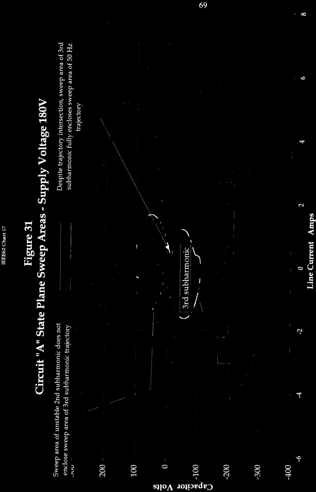
70 67 a ferrresnant state then the range f ferrresnant states culd be verestimated. This is definitely the case with circuit "A". 8.2 State Plane Analysis Three state variables are required t describe behaviur f the series cmpensated circuits "A" and "B". These can be selected as: line current capacitr vltage transfrmer primary current The transfrmer current and the line current are almst identical with the small difference being due t the effect f the 1500 hm resistr used t represent the transfrmer n lad lsses. Based n the assumptin that the line and transfrmer currents are apprximately equal, circuits "A" and "B" can be represented by tw state variables. The state variables are line current and capacitr vltage Figure 30 shws the phase plane trajectries f circuit "A" at a supply vltage f 180 vlts RMS. Shwn are the 50Hz trajectry, 3rd subharmnic trajectry and the unstable 2nd subharmnic slutin frm the frequency dmain mdel. It shuld be nted that the unstable 2nd subharmnic slutin culd nt be achieved in the labratry r in the time dmain mdel. Figure 31 shws the sweep areas f each f the trajectries. Series Cmpensatin f Distributin and Subtransmissin Lines
 l CO O!-!")
71 68 r bfj > > O rh rt +» *t LO U CN w w w l-h ti OH OH (/) l CO O!-! CD VH CU VH U ti CU IH rt ti, VH cu ti rt l-h t CU rt CD CN CM cn s 3 U cu c 1-1 HJ ti u VH u vo s *l A Jaipwh


72 J u SHJJOA mpvdvr)
73 In circuit "A" it can be bserved that the trajectry sweep area f the unstable 2nd subharmnic n the phase plane des nt ttally enclse the trajectry sweep area f the 3rd subharmnic. It can als be bserved that the 3rd subharmnic trajectry and the 50Hz trajectry intersect n the phase plane. Despite the trajectry intersectin, the 3rd subharmnic sweep area cmpletely cntains the sweep area f the 50Hz trajectry because the 3rd subharmnic trajectry lps within itself Figure 32 shws the state plane trajectries f circuit "B" at a supply vltage f 240 vlts RMS. Shwn are the 50Hz trajectry, 3rd subharmnic trajectry and the 2nd subharmnic trajectry. Figure 33 shws the sweep areas f each f the trajectries In circuit "B" it can be bserved that the trajectry sweep area f the stable 2nd subharmnic n the phase plane ttally enclses the trajectry sweep area f the 3rd subharmnic. It can als be bserved that the sweep area f the 50Hz trajectry lies cmpletely within the 3rd subharmnic sweep area The state plane trajectries prvide an interesting view f the ferrresnance phenmenn. The state plane des nt give any indicatin f the supply vltage angle. Hence intersectin f different states n the state plane may ccur at cmpletely parts f the supply vltage wave. 8.3 Stability f Frequency Dmain Ferrresnant Slutins It is well dcumented and understd that a ferrresnant state will cease t exist when the Jacbian appraches zer [431]. Experimental and mdelling wrk has shwn that a frequency dmain ferrresnant slutin may be unstable in the time dmain and unachievable in the actual circuit. Series Cmpensatin f Distributin and SubUansmissin Lines
 rt Cfl pa ti u VH IH u CM lo ID dj 6 < cu & fl U cu ti un I LO tn i S")
74 71 u CO w w B > O CM P bo rt +» l-h > I H CH ti CD i CM * Qj) VH a 2 t t? CU C rt l-h t 0) rt Cfl pa ti u VH IH u CM lo ID dj 6 < cu & fl U cu ti un I LO tn i S H A JOjpedlQ

75 72 u m a > CM CU bc rt l-h > l-h PH CH ti CD CO < Figu weep CD CU ti rt l-h t OJ 4-i rt +* CD PH 4) 4 * in in 4 in O u C j>p PH ti a IH u CN LO LO 03 OH s O < ti E fl U cu ti LO I I s- (8 -fl fl in TJ C IN (fl 4 (H (8 OH 4 4 CD LO 8 I s Jl A JO pbd«3
76 It appears that ne frequency dmain slutin in sme way may interfere with anther ferrresnant slutin (at a different base frequency) making it unstable. This is particularly evident in the mdelled and measured results fr circuit "A" as shwn previusly in figure 19 with respect t the 2nd subharmnic The time dmain simulatin has been used as a reliable test f stability. Stability is achieved if the time dmain simulatin prduces steady repeating wavefrms ver a lng perid f time When the harmnic balance apprach is used, the mdel is blind t all frequencies that are nt multiples f the specified base frequency. It is nt surprising that when different base frequencies are used (e.g. 1/2 and 1/3 pwer frequency) that cnflicting slutins are btained where smetimes ne slutin predminates ver the ther Unstable frequency dmain slutins culd be related in sme way t state plane trajectry intersectins, state plain swept area intersectin r ther criteria. Further research culd lead t imprved methds f stability determinatin. Series Cmpensatin f Distributin and Subtransmissin Lines
77 74 9. Management f Ferrresnance and Shrt Circuit Withstand Initiatin f Ferrresnance in Series Capacitr Cmpensated Circuits In a nrmal distributin pwer system perating envirnment the generatin f ferrresnance in a series cmpensatin scheme under n-lad r light lad cnditins is likely unless effective cunter measures are taken. The previus results have shwn that ferrresnance can generate capacitr vervltages in the rder f 5 times nrmal full lad perating vltage. During ferrresnant states currents can be less than full lad current r in the rder f 5 times lad current and transfrmer vltage canrise abve 2 times nminal A substantial transient such as energising a transfrmer via a switch r circuit breaker is generally required t initiate a ferrresnant state. In a circuit withut effective cuntermeasures the ferrresnant state will cntinue indefinitely. It is the nging nature f ferrresnance that makes it particularly destructive The generatin f ferrresnance will nly ccur if the transfrmer is driven int saturatin and the transfrmer is in a n lad r light lad situatin. In the single phase case where the capacitr hlds n initial charge and the transfrmer has n residual flux, a vltage switch n time crrespnding t sine 90 degrees (vltage peak) will avid driving the transfrmer int saturatin and hence avid the nset f ferrresnance. A switch n time crrespnding t sine(0) (vltage zer) will drive the transfrmer int heaviest saturatin and is the switching angle mst likely t initiate ferrresnance Mdelling and experimental wrk has shwn that fr single phase circuits with n stred energy that are susceptible t ferrresnance, there is a critical Series Cmpensatin f Distributin and Subtransmissin Lines
78 75 switching time between sine 0 and sine 90 degrees belw which ferrresnance may be initiated. 5 If the capacitr hlds residual charge and/r the transfrmer hlds residua flux then the critical switching vltage angle can vary cnsiderably. In sme ferrresnant circuits the ferrresnant states cannt be initiated by nrmal switch n transient unless there is residual capacitr charge and/r transfrmer flux. In experimental circuits "A" and "B" this was the case fr the 2nd subharmnic states. 6 Figure 34 shws a very simple radial series cmpensatin scheme with a typical arrangement f switchgear. The mst likely standard switching prcedures that culd prvide the transient necessary t drive the system int a ferrresnant state are: a) Energising the transfrmer by clsing circuit breaker "X' with switches "Y" and "Z" clsed. b) Energising the transfrmer by clsing switch "Y" with circuit breaker "X' and switch "Z" clsed. c) Energising the transfrmer by clsing switch "Z" with circuit breaker "X" and switch "X' clsed. D cn X 1 1kV O.H. Line Y z Transfrmer CQ > Circuit Breaker Series Capacitr Figure 34 Simplified Series Cmpensated llkv Line Series Cmpensatin f Distributin and Subtransmissin Lines
79 These switching peratins are nrmal day t day pwer system peratins that are likely t ccur during substatin cmmissining, maintenance and restratin f supply after faults The use f aut reclsing at circuit breaker "X' is a prime candidate fr initiating ferrresnance and is wrthy f sme attentin. Aut reclsing is a technique used t cater fr shrt duratin transient faults. With aut reclsing, after a prtectin trip clears a line fault, the circuit breaker is autmatically reclsed after a predetermined time usually in the range 0.1 t 10 secnds. If the fault remains n the line the circuit breaker trips and lcks ut. If the fault is cleared the line remains energised after the reclse Aut reclsing is particularly prne t initiating ferrresnance because at the time f clearing the fault there is a wide range f residual capacitr charge and transfrmer flux cnditins pssible. When the clse ccurs the vltage angle can als vary ver a wide range creating cnditins that in many cases will be cnducive t ferrresnance. Anther factr that can be verlked is that the feeder lad may drp t near zer after a successful reclse. This can ccur because even a very brief interruptin f supply can result in mtr cntactrs drpping ut causing significant lad shedding in industrial plants and thrughut the supply area The transient and lad shedding characteristics f aut reclsing make it a majr cnsideratin in the initiatin f ferrresnance. 9.2 Shrt Circuit Fault Cnsideratins In any series cmpensatin scheme, careful cnsideratin needs t be given t the effect the series elements have n system fault levels. It is essential that all Series Cmpensatin f Distributin and Subtransmissin Lines


80 77 circuit elements are capable f sustaining the full shrt circuit cnditins fr a reasnable fault clearing time withut damage The use f series capacitrs can greatly increase the system fault levels because f the reduced verall system impedances. Table 3 shws the effect n the system fault level f the series capacitrs fr the experimental circuit "B". Table 3 Mdelled Shrt Circuit Fault Currents fr the Labratry Series Cmpensated Circuit "B" Cnfiguratin Cupimtw/LineCurrent N series cmpensatin 12 amps 6.0 p.u. With capacitr cmpensatin 35 amps 17.5 p.u. Ntes: - rated lad current is 2 amps - all currents are RMS quantities The table shws that in the labratry circuit the fault level at the transfrm primary terminals has increased by almst a factr f three (3). This can have a significant effect n the fault rating requirement f all pwer system cmpnents, especially n the fault rating f the series capacitr. Series Cmpensatin f Distributin and SubUansmissin Lines
81 The fault rating f the series capacitr is a majr cnsideratin. The shrt circuit perfrmance f capacitrs is restricted in terms f the thermal impact f shrt circuit current and the assciated vltage stresses [131]. Series Cmpensatin f Distributin and Subtransmissin Lines
82 Existing Techniques fr Managing Ferrresnance and Shrt Circuit Currents 10.1 ASEA Series Cmpensatin Circuit Arrangements f Figures 35 and 36 shw tw series capacitr schemes frm the 1954 ASEA Jurnal 102. One f the circuits is designed fr small series cmpensatin schemes where the cmpensatin is nt mre than a few hundred kvar while the ther is designed fr schemes in the rder f 1 t 2 MVAR The Simple ASEA Spark Gap Series Cmpensatin Circuit The spark gap in shwn in Figure 35 is set t perate when vervltages ccur acrss the capacitr. In this circuit it is difficult t set the spark gap threshld vltage high enugh t cater fr nrmal lad currents yet lw enugh t prvide sufficient capacitr prtectin fr thrugh faults and damping fr subharmnic scillatins. In additin, damage culd be caused by lw fault currents thrugh the spark gap that may nt be cleared by the high vltage feeder prtectin. This circuit is quite simple but it has inherent limitatins The series cmpensatin scheme shwn in Figure 36 utilises a by-pass circuit breaker, spark gap, damping resistr and special prtectin relays When subharmnic ferrresnant disturbances ccur, the secndary winding f the vltage transfrmer cntains subharmnic vltages. The subharmnic vltage is sensed using a lw pass filter. After sensing the subharmnic vltage fr a brief perid f time the prtectin scheme clses the circuit breaker t place the damping resistr in parallel with the capacitr. The resistr then damps ut the subharmnic scillatins. After the prtectin Series Cmpensatin f Distributin and Subtransmissin Lines
83 80 senses that the subharmnic scillatins are remved the circuit breaker is pened and the circuit returns t nrmal peratin. damping resistr spark gap series capacitr bypass <^> switch ure 35 ASEA Series Capacitr Circuit fr nt mre than few hundred kvar bypass switch -0"Odamping resistr spark gap current transfrmer Figure 36 ASEA Series Capacitr Circuit fr 1-2 MVAR Series Cmpensatin f Distributin and Subtransmissin Lines


84 The ASEA By-pass Circuit Breaker Circuit During line shrt circuit cnditins, the capacitr experiences a large vltage rise. The vltage rise causes the prtective spark gap t arc acrss. The arc discharges the capacitr thrugh the damping resistr. The prtectin senses the fault current via the current transfrmer and then clses the circuit breaker. The clsed circuit breaker extinguishes the arc t prtect the spark gap. The shrt circuit withstand prcess invlves three (3) distinct stages. Stage 1: Stage 2: Stage 3: All fault current is carried by the capacitr. Fault current is shared between the capacitr and the spark gap. Fault current is shared between the capacitr and the circuit breaker This circuit is mre rbust that the previus circuit but it is cnsiderably mre expensive due t the added cst f circuit breakers, vltage transfrmer, current transfrmer and prtectin relays Mdern Day Series Capacitr Arrangements fr Distributin Lines The fundamental techniques develped in 1954 are used by ASEA Brwn Bveri tday in their "Minicap" series cmpensatr fr distributin [134]. Figure 37 shws the circuit arrangement fr a typical "Minicap" installatin In the mdern circuit arrangement the vacuum bypass switch clses n the lss f supply vltage t ensure the capacitr is bypassed when the circuit is energised. This minimises therisk f ferrresnance during turn n and feeder aut reclse. The system incrprates a precisin triggered spark gap that is used t initiate an instantaneus clse f the vacuum bypass switch as sn as an arc develps. Series Cmpensatin f Distributin and Subtransmissin Lines
85 82 -O^b- -^bseries capacitr -&^vltage transfrmer arc detectr dischage limiting inductr spark gap O^Ovacumm bypass switch - electrically perated Figure 37 ASEA Brwn Bveri Minicap - Typical Arrangement The "Minicap" system has a discharge limiting inductance t limit the discharge current f the capacitr when the bypass is initiated. In additin the system incrprates sphisticated resnance detectin equipment t prtect the system frm vervltages generated ferrresnance, self excitatin f mtrs and pwer frequency resnance The system described tends t be relatively expensive cmpared t line augmentatins and ther slutins t distributin vltage regulatin prblems. This thesis is cncerned with examining the pssibility f achieving series capacitr cmpensatin at the distributin level using a different apprach invlving simpler and less expensive cmpnents. Series Cmpensatin f Distributin and Subtransmissin Lines
86 A New Technique fr Managing Ferrresnance 11.1 Areas fr Ptential Imprvement f Existing Series Cmpensatin Arrangements Mdelling and experimental wrk with series cmpensated circuits have shwn what majr prblems ferrresnance and shrt circuit currents can be. The fundamental apprach t vercming these prblems has ften been t use prtectin devices t sense abnrmal cnditins f ferrresnance and shrt circuit and then bypass the capacitr with a switch r circuit breaker t prtect the capacitr This apprach requires expensive prtectin sensing equipment, switches/circuit breakers and ther related equipment. During nrmal peratin the circuit always remains susceptible t ferrresnance and heavy shrt circuit current. It is nly when abnrmal cnditins are sensed by the prtectin that the circuit is altered t cunteract the prblems New techniques that can address the ferrresnance and shrt circuit issues with less prtectin equipment and reduced hardware requirements ffer great ptential benefits fr the electricity supply industry Series Cmpensatin With Saturable Chke And Damping Resistr Figure 38 shws a series cmpensated circuit cnfiguratin with a damping resistr and saturable chke. The transfrmer has a saturable irn cre. The pwer line supplying the transfrmer is represented by a linear inductance "L" and resistance "R". The circuit cntains a series capacitr t tune ut the effects f the line inductance. The capacitance will nrmally be chsen s as t tune ut all r mst f the line inductance at the pwer frequency. Series Cmpensatin f Distributin and SubUansmissin Lines
87 84 Damping Resistr Saturating Chke VI Vr ^nr v A/w L R Rd Xc Vc V(-t) Figure 38 Series Cmpensated Circuit with Damping Resistr and Saturable Chke The use f a saturable chke in cnjunctin with the damping resistr is the innvative aspect f the circuit. Extensive mdelling f this circuit shws that it has prperties that are well suited t series cmpensatin f distributin lines Thery f Operatin The fundamental aspect f the series cmpensatin circuit is that all circuit elements f the series cmpensatr are permanently cnnected in the circuit. There are n switches r circuit breakers and n prtectin relays Under emergency full lad cnditins the vltage acrss the capacitr will typically reach 20% f the supply vltage. The saturating chke is designed such that at full emergency line lading, the knee pint f the chke is sufficiently high s as nt t interfere with the nrmal peratin f the capacitr. Hence under nrmal perating cnditins the chke draws nly a Series Cmpensatin f Distributin and SubUansmissin Lines
88 85 small magnetising current and the capacitr effectively carries all the lad current. This prvides the line with the desired cmpensatin effect Under cnditins f subharmnic ferrresnance the capacitr vltage increases substantially abve the knee pint driving the chke int saturatin. During saturatin the chke lks like a shrt circuit which effectively places the damping resistr in parallel with the capacitr. Careful selectin f cmpnents can eliminate the undesirable ferrresnant states. The lw frequency cmpnents f the subharmnic ferrresnance als assists with saturating the chke Under fault shrt circuit cnditins n the lad side f the series cmpensatr the capacitr vltage rises substantially abve nrmal causing the chke t saturate. During the parts f the cycle where chke is saturated the damping resistrs are effectively in parallel with the capacitr. This has the effect f reducing the verall line fault current and substantially reducing the fault current carried by the capacitr One f the significant circuit aspects f the saturable chke is that it prvides a path fr D.C. current t be bypassed arund the capacitr. The lcatin f the saturating chke ensures that the series capacitr hlds n steady state D.C. cmpnent f vltage/charge. The circuit arrangement frces any D.C. cmpnent f capacitr charge t be discharged via the damping resistr and saturating chke. Trapped D.C. capacitr charge causes pwer transfrmer saturatin which can lead t the nset f ferrresnance Mdel and Experimental Results with the Series Cmpensatr Labratry circuit "B" described earlier in this thesis was used as the base circuit n which t test the series cmpensatr technique. Figure 39 shws the series cmpensated circuit that was mdelled and cnstructed in the labratry. Series Cmpensatin f Distributin and SubUansmissin Lines
89 86 Rd=19.1 DHM lllz? ±lnq rvvv^t) ic Xc(ic) L = 0.054H >\ \A, V(t) R = 5,6 QHM C = 182uF Vp XCi) Figure 39 Labratry Series Cmpensated Circuit with Saturating Chke The saturable chke was designed with a 50 hertz knee pint vltage sufficiently high t permit emergency full lad peratin yet lw enugh t prvide effective damping. Experimental wrk fund that the saturating chke culd be mdelled by equatin (16). Details f the mdelled and experimental saturating chke results are shwn in Figures 40 and 41. ic(^c) = 0.8X, C X c 9.(16) The circuit was mdelled t determine the ptimum damping resistr value t eliminate the unwanted ferrresnant states. Mdelling shwed that if the hmic value was t high r t lw the ferrresnant states wuld be mdified but nt eliminated. A damping resistr value f 19.1 Q was selected and inserted int the labratry circuit. Series Cmpensatin f Distributin and SubUansmissin Lines


90 87

 ;uaxin3")
91 OJ U bo fi IH CO & OJ O U «3 a> c fi s OJ 2 a CO U c CO *J 1 ( O KJ > bo > U a> Tx tx (SIVH sdure) ;uaxin3 SuisfiraSBiv
92 Insertin f the damping resistr and saturable chke was cmpletely effective in eliminating the ferrresnant states. Figure 42 shws bth the mdel predicted and labratry variatin in R.M.S. current ver a range f applied surce vltages at n lad. Bth the 3rd subharmnic ferrresnant state and the 2nd ferrresnant state have been eliminated. The riginal 3rd subharmnic ferrresnant and the 2nd ferrresnant states can be clearly seen in the results f the uncmpensated circuit in Figure The chke and damping resistr prevented the establishment f ferrresnance fllwing every switching transient attempt t excite the circuit int a ferrresnant state In additin the labratry circuit was brught int a range f ferrresnant states withut the saturable chke cnnected. While the circuit was in the ferrresnant state the saturable chke and damping resistr were cnnected t the circuit. The cnnectin f the saturable chke and damping resistr eliminated the ferrresnance in every case Mdelled Transient Respnse f Labratry Circuit The previus experimental and mdelling results have shwn hw the saturable chke can eliminate the steady state 3rd subharmnic and 2nd subharmnic ferrresnant mdes. The effectiveness f the saturable chke can be demnstrated by examining switch n transients that wuld nrmally lead t ferrresnance When energising transfrmers, a zer vltage switch n angle is the mst severe starting cnditin with respect t transfrmer saturatin and inrush currents. Fr a series cmpensated circuit at rest (i.e. n stred energy), a switch n at vltage zer is the cnditin mst likely t initiate ferrresnance because f the transfrmer saturatin and inrush current effects. Series Cmpensatin f Distributin and SubUansmissin Lines

 JjuaxinD")


93 OJ M 0 u bo fi rt rt CD OJ *g 5b QQ ih 3 u IH u 4-» fi OJ 5 (X) i c ''! 1 :! 3 c OJ 1 _ s i C i O- ; a> 1 ' IH SH I <V 0J ] 1 X X 1 i 'mm c 01 X ai t_ CH 09 a H c 0 V) OJ Ci 0 IH IH Qj PH "0 HI r v. 0 -a c IS :.;:.:.; j j- -; -- -j I O 1 i a c CO (sdine) JjuaxinD S'pV'H ::: /. -.- qj fl SH - - u ~3 TJ Pi. d \ V / QJ " > >^1 5-1 S3 u s PH IH QJ ~ s S- H c (0 SH / 1 1 I - - H TJ aj (8 K Pi -! \ j \ 1 \ "~~~l>n O E CN i C 5 c 5 C 0 Q3 1 0l r f Z fr li3 r\/x~7 003 \ OZl 09l lst In 0 t l3t AT T ULL 0UL OZ - 09 OS Ofr 0 03 n u
94 Figure 43 shws the simulated respnse t a zer vltage switch n withut the saturable chke in place. The figure shws that after a brief transient f apprximately five (5) cycles, a stable 3rd subharmnic ferrresnance is established and cntinues indefinitely Figure 44 shws the simulatin f the same series cmpensated circuit with the saturable chke and damping resistr added. The saturable chke and damping resistr have the effect f damping ut the switch n transient in a way that des nt permit the establishment f steady state ferrresnance. At 0.6 f a cycle after switch n the chke current peaks at 4.1 amps and then returns permanently t near zer amps after tw (2) cycles. It is the ability f the chke t prvide a D.C. current path that makes the scheme s effective Cmparisn f the tw (2) switch n transients shw clearly the effectiveness f the saturable chke and damping resistr in eliminating ferrresnance Fault Shrt Circuit Perfrmance Mdelling has shwn that the chke and damping resistr characteristics can be effectively used t cntrl and limit the system fault levels. Table 3 illustrated this pint using the labratry circuit under different cnfiguratins Table 4 illustrates hw the saturable chke and damping resistr can be used t cntrl system fault levels. The fault currents referred t are fr a shrt circuit at the transfrmer terminals with a 200 vlt RMS supply. The table shws that the additin the capacitr t the uncmpensated circuited increases the fault level frm 6 p.u. t 17.5 p.u.. This is a very large increase and is the direct result f the pwer frequency tuning effect f the capacitr with the line inductance. Series Cmpensatin f Distributin and SubUansmissin Lines

 fi b")


95 OJ O X u WD fi l-h rt 3 rt (X) fi b fi u rh u OJ IH CO fi rt H fi <J IH CD sjaqam P UB sdury


96 OJ O X u bo fi lh rt rh fi rt CD g)g M H fi IH CD fi OJ IH CO fi rt u sduiy


97 94 Table 4 Mdelled Shrt Circuit Fault Currents fr the Labratry Circuit "B" Capacitr Chke Current Current P.U. P.tL N series cmpensatin Capacitr nly N/A 17.5 N/A ill Capacitr & chke Ntes:- rated lad current is 2 Amps = 1 P.U. - all currents are RMS quantities When the chke and damping resistr are added t the series capacitr the chke heavily saturates under fault cnditins causing a substantial circulating current in the capacitr/chke lp. In this situatin the line fault current is reduced t 5.5 p.u. which is apprximates the value f the line fault current in the uncmpensated case. Series Cmpensatin f Distributin and SubUansmissin Lines
98 Selectin Of Cmpnent Values 12.1 General Rules fr Cmpnent Selectin On first inspectin the selectin f cmpnent values appears t be difficult requiring extensive mdelling f each individual situatin. Mdelling and analysis f a number f circuit cnfiguratins has shwn that selectin f cmpnent values can be relatively straightfrward by the use f the fllwing rules Capacitr pf Selectin T achieve full cmpensatin the capacitr value "C" shuld be selected t give the same reactive impedance as the line inductance at the pwer frequency. i.e. fr full cmpensatin C=1/(LQ 2 ) (17) There are stability advantages in designing fr less than full cmpensatin. Depending n the actual design situatin, engineers may elect t less than fully cmpensate fr the inductive reactance f the line Damping Resistr Ohmic Selectin Mdelling and experimental wrk has shwn that the damping resistr hmic value is critical t the effective perfrmance f the system. If the hmic value is t high then little current flws thrugh the chke/resistr resulting in ineffective damping under ferrresnant and fault cnditins. If the hmic value is t lw heavy currents flw thrugh the damping resistr under Series Cmpensatin f Distributin and Subtransmissin Lines
99 96 ferrresnant and fault cnditins but the I 2 R lss is t small t prvide effective damping Analysis and experimental wrk n the series cmpensatin scheme has shwn damping resistr hmic value shuld be selected t apprximately equal the reactive impedance f the capacitr at the pwer frequency. i.e. suggested Rj «1/( C) (18) The reasn fr this selectin is as fllws. Circuit damping is prvided by saturating the chke and generating I 2 R lsses in the damping resistr. Under cnditins f chke saturatin the chke can be thught f as a shrt circuit. Under these cnditins the capacitr discharges directly int the resistr with a time cnstant f RjC. At the suggested value f Rj this time cnstant is 1/c r 1/27C (apprximately l/6th) f a perid. Under cnditins f ferrresnance in the pwer line circuits the time perid f high capacitr vltage is typically half t ne perid r 3.5 t 7 R^C time cnstants. This is generally sufficient time fr the damping resistr t sufficiently discharge the capacitr and prevent the nset f ferrresnance If Rd is t large the Capacitr damping resistr time cnstant is t lng t allw effective damping. If Rd is t small the leakage reactance f the saturating chke becmes significant limiting the circulating current and hence the I 2 R effect f the damping resistr After selectin f a damping resistr value R^ it is imprtant t mdel the series cmpensatin scheme t check that all ferrresnant states have been eliminated. Series Cmpensatin f Distributin and SubUansmissin Lines
100 Saturable Chke There are a number f aspects f the saturating chke that require careful design cnsideratin Knee Pint The knee pint f the saturable chke must be sufficiently high t permit nrmal and emergency lads withut any saturatin effects. Hwever fr currents in excess f the emergency lad plus a safety margin the chke must g heavily int saturatin Leakage Inductance The leakage inductance is the marginal inductance f the chke when it is in full saturatin. The leakage inductance must be sufficiently small s as nt t interfere with the discharge f the capacitr int the damping resistr. The ideal value wuld be zer henries T achieve the desired effect the natural frequency f the capacitr in cmbinatin with the leakage reactance f the chke (L c j) must be much greater than the pwer frequency. l/sqrt(l cl C)» ( 19) r L cl «1/(C 2 ) (20) Series Cmpensatin f Distributin and SubUansmissin Lines
101 Scaling Up T Real Distributin Netwrks 13.1 Limitatins f Small Scale Labratry Experiments The experimental results have been successful in determining the effectiveness f the mdelling and prviding practical insight int the issues assciated with series cmpensatin. The limitatin f the experimental wrk has been ne f scale. The experimental wrk has been dealing with circuits with a supply vltage f 240 vlts and lad currents f 2 amps T be effective in practice, the prpsed series cmpensatin scheme needs t perate fr a supply vltage f 1 lkv and up and lad currents f 10 amps up t 1000's f amps. Testing and experimenting n this scale has simply nt been pssible The questin arises, are the cmpnent values and ratings required fr real series cmpensatin scheme within the realm f engineering practicability? T answer this questin a circuit with realistic distributin values was mdelled and the cmpnent values and ratings determined The single phase circuit t be mdelled is shwn in Figure 45. The nminal supply vltage was llkv and the maximum emergency line lad was 262 amps. Wrst case cnditins were examined including n lss distributin transfrmers with sharp saturatin curves. The line has 11% full lad vltage regulatin at 0.85 pwer factr. Series Cmpensatin f Distributin and SubUansmissin Lines
102 99 Rd = 6.28 DHM s - aturq+in 9 Chke L = 0,02H IC Xc(ic) R=l,55 DHM C=507uF V(t) nminal llkv 1 phase Figure 45 Large Scale Series Cmpensated Circuit with Saturating Chke Circuit "C" The chke and transfrmer characteristics used are detailed in equatins belw. The transfrmer lsses were represented by a 14,400 hm resistance acrss the transfrmer llkv terminals. The transfrmer characteristics were based n cmmercially available mdern pwer distributin transfrmers. i = X " 30 X 17 (21) i c = A, c (22) This circuit prvides full cmpensatin and reduces the line vltage drp frm 11% t 3%. In distributin netwrks, the length f line, number f transfrmers and lading can vary greatly with changes t the switching cnfiguratin and the cnstructin f additins t the system ver time. Series Cmpensatin f Distributin and SubUansmissin Lines
103 The mdelled characteristics f the system are described in the fllwing figures. Figure 46 N Lad Ferrresnant States with n Saturating Chke Cmpensatin. Figure 47 Shrt Circuit Fault level Cmparisns with and withut Cmpensatin. Figure 48 Capacitr vltage with and withut Cmpensatin under Shrt Circuit Fault Cnditins. Figure 49 Chke, Capacitr and Line currents under shrt circuit fault cnditins The mdelling clearly demnstrates that the damping chke limits the fault duty f bth the line and capacitr. Further mdelling als shwed that the ferrresnant states were eliminated Equipment Rating Based n the mdelling, the fllwing ratings were devised fr Circuit "C" Vsrc= 11,000 vlts L=0.02 H RL=1.55hm 1 phase Series Capacitr C=507 pf Cntinuus rating 200 amps rms (252 kvar) 1,256 vlts rms 1,775 vlts peak Series Cmpensatin f Distributin and SubUansmissin Lines


104 101 c OJ rt CD fi rt fi O c OJ u O ft OJ PJH OJ l-h O & OJ CO CD OJ l-h rt <j CD SP rt DO vd O < * <N SPMH sdray


105 102 IN <* CO fi O CO IH u rt D< & O U fi rt SWH sduiy lin«j


106 103 8 ' > 1 4 CM Cm c CN SW& asbj[ A rajped^


107 0 rt u IH u X CD h OJ -a fi P fi CO OJ ih.2 1 *» fi +j *d a Si u I E OJ + > CO >> CD a OJ rt c fi OJ & O U OJ u W3 OJ > a CM s CO SPVH sdray juaui jpre j
108 105 3 hur rating 263 amps rms (435 kvar) 1,651 vlts rms 2,335 vlts peak 3 secnd fault rating 1,754 amps rms 2,547 amps peak 10,466 vlts rms 15,677 vlts peak Damping Resistr 6.28 hm 3 secnd rating 1454 amps rms (13.3Mw) 2481 amps peak Saturable Chke 3 secnd rating 1,454 amps rms 2,481 amps peak Series Cmpensatin f Distributin and SubUansmissin Lines
109 Cmments n the Cmpnent Specificatins The required ratings f system cmpnents indicate that they are within the realm f engineering reality The cntinuus rating f the capacitr is readily achievable. The difficulty in ecnmically cnstructing such a capacitr is prviding fr the 3 secnd fault rating. This is a fundamental prblem f series cmpensatin schemes. It shuld be nted that the cmpensatin arrangement nt nly eliminated the ferrresnance prblem but als reduces the capacitr's 3 secnd rating frm 7,000 amps (uncmpensated) t 1,900 amps (cmpensated). The damping chke imprves the ecnmic feasibility f cnstructing a suitable capacitr by a great margin There wuld be n majr technical prblems in the cnstructin f the saturating chke r the damping resistr. Ple munting f all the equipment is envisaged Ferrresnance Prtectin In rder t prvide additinal prtectin t the distributin netwrk and the electricity custmers, subharmnic ferrresnance prtectin culd be cnsidered. Figure 50 shws a methd f subharmnic ferrresnance prtectin which culd be prvided. / Lw Pass Filter Ferrresnant Detectin Relay Saturating Chke Trnsfrmer(s) 3 DO 11 kv O.H. Line A *S* t Q- Zne Substatin Circuit Breaker Series Capacitr metering class current transfrmer Figure 50 Prpsed Ferrresnant Prtectin Scheme Series Cmpensatin f Distributin and SubUansmissin Lines
110 The subharmnic prtectin relay wuld incrprate a lw passfilter and cause the llkv circuit breaker t perate if subharmnic currents were detected. Such a scheme wuld use existing feeder circuit breakers and culd be incrprated at relatively lw cst Subharmnic prtectin wuld prvide added security t the scheme and prvide sme backup prtectin n the damage t either the saturating chke r the damping resistr. Series Cmpensatin f Distributin and SubUansmissin Lines
111 Future Research Directins 14.1 The Need fr Field Trials Further research int the prpsed series cmpensatin scheme requires field trials at 1 lkv r similar vltages. There are limitatins and inherentrisksin scaling up the results f small scale labratry experiments t larger real pwer systems. Large scale systems tend t have transfrmers with lwer lsses and sharper saturatin characteristics. In many cases real pwer systems have high line X/R ratis that are difficult t reprduce at small scale Fr these reasns larger scale field trials are cnsidered the next lgical s in the research and develpment prcess The Likelihd f Universal Slutins Mdelling f a number f systems suggests that the use f the cmpnent selectin techniques described in sectin 11 culd eliminate the need t mdel each individual applicatin. Further mdelling and actual field trials are necessary t draw any definite cnclusins n the issue Three Phase Systems The saturating chke technique in the three phase situatin has a great deal ptential. Analysis f the three phase system has nt been attempted in any depth A three phase ferrresnant labratry circuit was cnstructed using cmpnent values that mdel a realistic three phase distributin line. A number f cmplex subharmnic wavefrms were generated. Of particular interest was the fact that the saturating chke technique with damping resistr was able t eliminate all the ferrresnant states. These preliminary results are Series Cmpensatin f Distributin and SubUansmissin Lines
112 109 very encuraging and shw that additinal mdelling f three phase systems is likely t lead t successful series cmpensatin using the saturating chke technique n three phase lines. Appendix E shws details f the three phase labratry circuit "D" cnstructed Stability Criteria fr Ferrresnance Frequency Dmain Slutins Time dmain mdelling has been used with success as a test fr the stability f frequency dmain slutins. Stability f a frequency dmain slutins is cnfirmed when the slutin can be mdelled in the time dmain as a steady repeating wavefrm ver a lng perid f time Opprtunities exist fr further research int causes f instability and imprved testing fr stability. Series Cmpensatin f Distributin and SubUansmissin Lines
113 Cnclusins 15.1 The Benefits f Series Cmpensatin Increasing the pwer carrying capacity f transmissin and distributin lines by series cmpensatin ffers great ptential fr electricity supply authrities. Effective series cmpensatin can reduce vltage regulatin in distributin and transmissin systems and prvide an effective cuntermeasure t vltage dips caused by lad fluctuatins Mdelling the Ferrresnance Phenmenn The mdelling and experimental wrk presented has highlighted the damaging ferrresnant vervltages and vercurrents that can be created by series capacitrs interacting with transfrmers. A thrugh understanding f the pssible ferrresnant mdes f behaviur is essential when cnsidering series cmpensatin f distributin and subtransmissin lines The Time Dmain and Frequency Dmain Ferrresnant Mdels have prved t be very useful and accurate. The mdels give the design engineer a valuable insight int the ferrresnant phenmenn as applicable t series cmpensatin and ther situatins. Fr engineers designing and studying the feasibility f series line cmpensatin the mdels ffer the ability t: determine the pssibility f ferrresnant vervltages and currents. determine the pssible mdes f ferrresnant behaviur. determine under what range f perating cnditins ferrresnance can ccur. Series Cmpensatin f Distributin and SubUansmissin Lines
114 Ill develp and analyse strategies fr eliminating ferrresnant cnditins The generatin f pwer system even subharmnic ferrresnant states was demnstrated bth experimentally and by mdelling in the demnstratin circuits. The generatin f even harmnic vltages and fluxes is mst unusual in pwer systems because f the linear nature f mst system cmpnents and the symmetry f transfrmer B-H lps. Even harmnic generatin resulted frm nn-symmetrical circuit behaviur, the key element f which was the existence f a DC cmpnent f transfrmer flux linkage. The mdels als predicted the existence f dd ferrresnant harmnics in the experimental circuits. Experimental wrk cnfirmed the existence f all the predicted ferrresnant states The ferrresnant states assciated with series cmpensated transmissin and distributin lines can be mdelled and understd. Understanding and mdelling the phenmenn is the key t designing effective cuntermeasures A New Methd f Managing Series Cmpensatin A methd f eliminating ferrresnance in series cmpensated lines has been prpsed, mdelled and fund t be effective in a small scale series cmpensated labratry circuit. The mdelling and experimental wrk presented has highlighted hw ferrresnant vervltages and vercurrents can be eliminated by the use f a saturable chke and damping resistr The key t designing a successful scheme is t determine by mdelling the natural ferrresnant states. This mdelling is generally required ver a wide range f supply cnditins. Having determined the natural ferrresnant states, additinal mdelling f the system incrprating the saturable chke Series Cmpensatin f Distributin and SubUansmissin Lines
115 112 and damping resistr are required t ensure that all natural ferrresnant states are eliminated and that n new states are created The perfrmance f the system under transient and shrt circuit cnditins is f critical imprtance and needs t be cnsidered at the early design stage. Fault levels can be cntrlled within limits t suit the designer's requirements The saturable chke technique is simple, effective and requires n sphisticated cntrl, prtectin r bypass switch systems. The chke and damping resistr technique is a nn-linear slutin t a cmplex nn-linear prblem. With further research the technique pens the way fr the mre widespread use f series capacitrs in distributin and subtransmissin electric pwer systems Cmpnent Values Simple techniques fr selecting cmpnent values have been develped that with additinal mdelling and experience may lead t universal general purpse series cmpensatin slutins. Field trials and additinal mdelling are required t make further prgress. Series Cmpensatin f Distributin and SubUansmissin Lines
116 References 16.1 Authr's Papers [1] R.A.Barr, "A Nmgram fr the Selectin f Matching Design Parameters fr the Undergrund Residential Distributin f Electricity" Jurnal f Electrical and Electrnics Engineering, Australia. Vl. 3, N. 2 June 1983, pp [2] A. Baitch and R.A.Barr, "A Tapping Range and Vltage Level Analysis Chart fr Tap Changing Transfrmers" IEEE Transactins n Pwer Apparatus and Systems, Vl. PAS-104, N. 11, Nvember 1985, pp [3] RABarr and D. Piatt, "Vltage Regulatin in Pwer Transfrmers by the Cntrl f Leakage Flux" IEEE Cnference paper - Cnference n Electrmagnetic Field Cmputatin held at Washingtn, D.C. U.S.A. December [4] R.A. Barr and D. Piatt, "A Temperature Cntrlled Nn-Linear Chke" Prceedings f the Australasian Universities Pwer Engineering Cnference held at Wllngng N.S.W. Australia, September 1993, Vl. 2, pp [5] R.A. Barr and D. Piatt "Mdelling and Mapping Ferrresnant States in Series Cmpensated Distributin and Subtransmissin Lines" IEEE Transactins n Pwer Delivery, Vl. 11, N.2, April 1996, pp [6] R.A. Barr and D. Piatt "Use f a Saturating Chke in the Series Capacitr Cmpensatin f Distributin Lines" IEE Prceedings n Generatin, Transmissin and Distributin, Vl. 143, N.6, Nvember Series Cmpensatin f Distributin and Subtransmissin Lines
117 Series Cmpensated Lines [101] W.G. Shepard, "AC Vltage Regulatin with Ordinary Transfrmers" Electr July 1953, pp [102] S. Smedsfelt and P. Hjertberg, "Series Capacitrs fr Distributin Netw ASEA Jurnal, Vl. 27, September 1954, pp [103] E.F. Kratz, L.W. Manning and M. Maxwell, "Ferrresnance in Series Capaci Distributin Transfrmer Applicatins" Trans. Amer. I.E.E. (P.AS), Vl. 78, Pt 3A, August 1959, pp [104] V. Madzarevic, "Ease Overvltages Due t Faults" Electrical Wrld, Augus 1977, pp [105] F. Ilicet and E. Cinieri, "Cmparative Analysis f Series and Shunt Cmpensatin Schemes fr AC Transmissin Systems" IEEE Transactins n Pwer Apparatus and Systems, Vl. PAS-96, N. 6, Nvember/December 1977, pp [106] J.L. Bath, J.E. Hardy and N. Tlmunen, "Series Capacitr Installatins B.C. Hydr 500kV System" IEEE Transactins n Pwer Apparatus and Systems, Vl. PAS-96, N. 6, Nvember/December 1977, pp [107] V. Madzarevic, F.K. Tseng, D.H. W, W.D. Niebuhr and R.G. Rcamra, "Overvltages n EHV Transmissin Lines Due t Faults and Subsequent Bypassing f Series Capacitrs", IEEE Transactins n Pwer Apparatus and Systems, Vl. PAS-96, N 6, Nvember/December 1977, pp Series Cmpensatin f Distributin and SubUansmissin Lines
118 115 [108] A.L. Curts, N.G. Hingrani and G.E. Stemler, "A New Series Capacitr Prtectin Scheme Using Nn-Linear Resistrs" IEEE Transactins n Pwer Apparatus and Systems, Vl. PAS-97, N. 4, July/August [109] E.R. Taylr, "Applicatin f Series Capacitrs" Electrical Engineer, Octber 1978, pp [110] S.C. Tripathy, K.K. Patel and M.Y. Khan, "Digital Cmputer Study f Switching Surges n Series Cmpensated Lines" Institutin f Engineers India Jurnal Electrical, Vl. 59, June 1979, pp [Ill] J.J. Burke, A.P. Engel and S.R. Gilligan, "Increasing the Pwer System Capac f the 50kV Black Mesa and Lake Pwell Railrad thrugh Harmnic Filtering and Series Cmpensatin" IEEE Trans. Pwer Apparatus and Systems, Vl. PAS- 98, N 4 July/Aug 1979, pp [112] E.E. Baraket and D.E. Hirst, "Susceptibility f 3-phase Pwer Systems f Fer nnlinear Oscillatins" IEE Prc. Vl. 126, N 12, December 1979, pp [113] C.A. Petersn and J.C. Osterhut, "Metal Oxide Prtectr fr Series Capacitr Installatins" Prceedings f the American Pwer Cnference, Vl. 42, 1980, pp [114] R.F. Wlff, "Metal Oxide Imprves Capacitr Prtectin" Electrical Wrld, March 1980, pp Series Cmpensatin f Distributin and SubUansmissin Lines
119 116 [115] G.T. Bellarmine and K. Srikrishna, "Optimum Cmpensatin with Series Capacitr at Centre f Transmissin Line" Institutin f Engineers India Jurnal Electrical, Vl. 60, June 1980, pp [116] N.T. Fahlein, "EHV Series Capacitr Equipment Prtectin and Cntrl" IEE Prc, Vl. 128, Part C, N. 6, Nvember 1981, pp [117] K. Murtani, K. Takenaka, M. Asan and M. Inuye, "Develpment and Testing f 500kV Series Capacitr", IEEE Transactins n Pwer Apparatus and Systems, Vl. PAS-101, N.7, July 1982, pp [118] T. Baitch, "Series Capacitrs Bst 1 lkv Line Perfrmance" Australian Elec Wrld, Vl. 47, N. 8, pp , August [119] Y. Mansur, T.G. Martinich and J.E. Draks, "B.C. Hydr Series Capacitr Ba Staged Fault Test" IEEE Transactins n Pwer Apparatus and Systems, Vl. PAS-102,N.7, July 1983, pp [120] S.P. Seth, "Cmparative Analysis f Shunt and Series Cmpensatin Schemes f 400kV Lines" Institutin f Engineers India Jurnal Electrical, Vl. 63, August 1983, pp [121] C.S. Indulkar, "Series Cmpensatin f EHV Transmissin Lines" Institutin Engineers India Jurnal Electrical, Vl. 65, Octber 1984, pp [122] A. Kalam, "Simulatin f Series Cmpensated EHV Transmissin Lines and Thei Prtectin" Institutin f Engineers India Jurnal Electrical, Vl. 60, December 1985, pp Series Cmpensatin f Distributin and Subtransmissin Lines
120 117 [123] Gldswrthy, "A Linearised Mdel fr MOV-Prtected Series Capacitrs" IEEE Transactins n Pwer Systems, Vl. PWRS-2, N. 4, Nvember 1987, pp [124] C.S. Indulkar and B. Viswanatnan, "Maximum Transfer Limited by Vltage Stability in Series and Shunt Cmpensated Schemes fr A.C. Transmissin Lines" IEEE Transactins n Pwer Delivery, Vl. 4, N. 2, April 1989, pp [125] Bn-Teck Oi, Shu-Zu Dai and Xia Wang, "Slid-State Capacitive Reactance Cmpensatrs" IEEE Trans. Pwer Delivery, Vl. 7, N. 2 April 1991, pp [126] G. G. Karady, "Cncept f a Circuit Current Limiter and Series Cmpensatr IEEE Trans. Pwer Delivery, Vl. 6, N. 3 July 1991 pp [127] M. El-Marsafawy, "Applicatin f Series-Capacitr and Shunt-Reactr Cmpensatin t an existing Practical AC Transmissin Line" IEE Prceedings-C Vl. 138, N 4, July 1991, pp [128] R. Vitelli, "Series Capacitrs in Distributin Systems" Reginal Cnferenc the Electricity Supply Engineers Assciatin f N.S.W. held at Narrabri, N.S.W. Australia 2-3 April [129] B.Oi, S Dai and X. Wang, "Slid State Series Capacitive Reactance Cmpensatrs" IEEE Transactins n Pwer Delivery, Vl. 7, N 2 April 1992, pp [130] S. G. Helbing and G.G. Karady, "Investigatins f an Advanced Frm f Seri Cmpensatin" IEEE Transactins n Pwer Delivery, Vl. 9, N.2, April 1994, pp Series Cmpensatin f Distributin and SubUansmissin Lines
121 118 [131] "IEEE Standard fr Series Capacitrs in Pwer System" IEEE Std [132] P. Halvarssn and L. Angquist, "Cntrlled Series Capacitrs - Practical and Ecnmical Slutins" Institutin f Engineers Australia, Prceedings f the Electrical Engineering Cngress held in Sydney Australia, Nvember 1994, pp [133] G. Ledwich and A. Ghsh, "Series Cmpensatin: Steady State Analysis" Institutin f Engineers Australia, Prceedings f the Electrical Engineering Cngress held in Sydney Australia, Nvember 1994, pp [134] ABB Pwer Systems, "Minicap Series Cmpensatin f Distributin Lines". Pamphlet A E 16.3 Ferrresnant Subharmnics [201] I. Travis and CN. Weygandt, "Subharmnics in Circuits Cntaining Irn-Cred Reactrs" Trans. Amer. I.E.E. (P.A.S.) August 1938, Vl. 57, pp [202] I. Travis, "Subharmnics in Circuits Cntaining Irn-Cred Reactrs IF'. Tra Amer. I.E.E. (P.A.S.), Vl. 58, 1939, pp [203] J.D. McCrumm, "An Experimental Investigatin f Subharmnic Currents" Trans. Amer. I.E.E. (P.A.S.), 1941, Vl. 60, pp [204] E. Brenner, "Subharmnic Respnse f the Ferrresnant Circuit with Cil Hysteresis" Trans. Amer. I.E.E. (P.A.S.), September 1956, Vl. 75, pp Series Cmpensatin f Distributin and Subtransmissin Lines
122 119 [205] LA. Wright, "Three Phase Subharmnic Oscillatins in Symmetrical Pwer Systems" Paper 70 TP 625-PWR IEEE Transmissin and Distributin Cmmittee May 1970, pp [206] LA. Wright and K. Mrsztyn, "Subharmnic Oscillatins in Pwer Systems Thery and Practice" Trans. IEEE (PAS) Vl. PAS 89, N. 8, Nvember 1970, pp [207] T.C. Cheng, "The Effect f Subsynchrnus Current n a Static Mh Type Distance Relay" IEEE Transactins n Pwer Apparatus and Systems, Vl. PAS- 100, N. 11, Nvember 1981, pp [208] A.S. Akpinar and S.A. Nasar, "Harmnic Balance Analysis f the Subharmni Ferrresnance" Electric Machines and Pwer Systems, Vl. 18, 1990, pp Ferrresnance Assciated with High Vltage Switching [301]E. Clarke, H.A. Petersn and P.H. Light, "Abnrmal Vltage Cnditins in T Phase Systems Prduced by Single-Phase Switching" Trans. Amer. I.E.E. (P.A.S.), 1941, Vl. 60, pp [302] G.G. Auer and A.J. Schultz, "An Analysis f 14.4/24.9kV Grunded Wye Distributin System Overvltages. Trans. Amer. I.E.E. (P.A.S.), August 1954, pp [303] L.B. Crann and R.B. Flickinger, "Overvltages n 14.4/24.9kV Rural Distr Systems" Trans. Amer. I.E.E. (P.A.S.), Octber 1954, pp Series Cmpensatin f Distributin and SubUansmissin Lines
123 120 [304] F.C. Van Wrmer, "Switching three-phase transfrmer banks" General Electric Mngraph March [305] R.H. Hpkinsn, "Ferrresnance During Single-phase Switching f 3-phase Distributin Transfrmer Banks" Trans. IEEE, April 1965, pp [306] A.M. Lckie, "Ferrresnance, a Grwing Prblem" Mngraph f unknwn USA rigin, March [307] R.H. Hpkinsn, "Ferrresnance During Single-Phase Switching f 3-Phase Distributin Transfrmer Banks" (Discussin). Trans. IEEE, June 1965, pp [308] J.F. Yung, "Ferrresnance - Prblems and Applicatins" Electrical Revie May 1965, pp [309] R.H. Hpkinsn, "Ferrresnant Overvltage Cntrl Based n TNA Tests n Three-Phase Delta-Wye Transfrmer Banks" Trans. IEEE (PAS) Vl. PAS-86, N. 10, Octber 1967, pp [310] R.H. Hpkinsn, "Ferrresnant Overvltage Cntrl based n TNA Tests n Three-Phase Delta-Wye Transfrmer Banks" IEEE (PAS) Vl. PAS-87, N. 2, February 1968, pp [311] F.S. Yung, R.L. Schrnid, and P.I. Fergetad, "A Labratry Investigatin Ferrresnance in Cable-Cnnected Transfrmers" Trans. IEEE (PAS), Vl. PAS-87, N. 5 May 1968, pp Series Cmpensatin f Distributin and SubUansmissin Lines
124 121 [312] R. Archibald, "160kV peaks ccur when Switching 13kV Circuits" Electrical Wrld, August 26, 1968, pp , 102. [313] G.C. Damstra, "Ferrresnance during Single-phase Switching" Electrical Engineer, 10 April, 1969, pp [314] G.C. Damastra, "Ferrresnance during Single-phase Switching f Distributi Transfrmers" Australian Electrical Wrld, May 1969, pp [315] A. Clerici and CH. Didriksen, "Dynamic vervltages and ferrresnance fund in switching. Trans. IEEE, August 1971, pp [316] E.J. Dlan, D.A. Gillies and E.W. Kimbark, "Ferrresnance in a Transfrmer Switched with an E.H.V. line" Trans. IEEE, May 1972, pp [317] G.D. Wale, "Ferrresnance in a Discnnected E.H.V. Pwer System" GEC Jurnal f Science and Technlgy, Vl. 40, N. 2, 1973, pp [318] A. Baitch, "Thery and Practice f Ferrresnance due t the Single Phase Switching f Distributin Transfrmers" Master f Engineering Thesis University f New Suth Wales, Australia [319] D.R. Smith and S.R. Swansn, "Overvltages with Remtely-Switched Cable-Fed Grunded Wye-Wye Transfrmers" IEEE paper T Nvember 1974, pp [320] A. Baitch, "Ferrresnance due t the Single Phase Switching f Distributin Transfrmers" Internatinal Cnference n Electricity Distributin Liege, Belgium 1979 Sessin 3 paper 24. Series Cmpensatin f Distributin and SubUansmissin Lines
125 122 [321] "Dual Prescriptin fr Ferrresnance" Electrical Wrld, May 1, 1979, pp [322] S. Prusty and M. Panda, "Predeterminatin f Lateral Length t Prevent Overvltage Prblems due t Open Cnductrs in Three Phase Systems" IEE Prc. Vl. 132, Pt. C, N. 1, January 1985, pp [323] J.R. Marti and A.C. Sudack, "Ferrresnance in Pwer Systems, Fundamental Slutins" IEE Prceedings-C, Vl. 138, N 4, July 1991, pp Ferrresnance Analytical Techniques [401] C.G Suits, "Studies in Nn-Linear Circuits" Trans. Amer. I.E.E. (P.A.S.) Ju 1931, pp [402] W.T. Thmsn, "Resnant Nnlinear Cntrl Circuits" Trans. Amer. I.E.E. (P.A.S.) August 1938, Vl. 57, pp [403] P.P. Odesseyt and E. Weber, "Critical Cnditins in Ferrresnance" Trans. Amer. I.E.E. (P.A.S.)August 1938, Vl. 57, pp [404] W.T. Thmsn, "Similitude f Critical Cnditins in Ferrresnant Circuits" Trans. Amer. I.E.E. (P.A.S.) Vl. 58, March 1939, pp [405] J.T. Salihi, "Analysis f Instability and Respnse f Reactrs with Rectang Hysteresis Lp Cre Material in Series with Capacitrs" Trans. Amer. I.E.E. (Cmrn. & Electrnics), July 1956, pp [406] G.E. Kelly, "The Ferrresnant Circuit" Trans. IEEE, January 1959, pp p Series Cmpensatin f Distributin and SubUansmissin Lines
126 123 [407] J.T. Salihi, "Thery f Ferrresnance" Trans. IEEE, January 1960, pp [408] L. Clarke, G.A. Curtis and R.O.M. Pwell, "Capacitrs in Relatin t Trans Fluctuating and Distrting Lads" Prc. IEE, 1963, pp [409] L.A. Finzi and A. Lavi, "The Cntrlled Ferrresnant Transfrmer" Paper ATEE Nn-Linear Magnetics Cmmittee January 1963, pp [410] R. Balasubramanian and D.P. Athertn, "Predictin f Jump Resnance in Systems Cntaining Certain Multidimensinal Nnlinearities" Prceedings IEE, Vl. 115, N. 9, September 1968, pp [411] G.W. Swift, "An Analytical Apprach t Ferrresnance" Trans. IEEE (PAS), Vl. PAS 88, N. 1, January 1969, pp [412] S.S. Lamba and R.J. Kavanagh, "Jump-Resnance Criteria fr Systems Cntai Duble-Valued And Frequency Dependent Nn-Linearities" Prceedings IEE, Vl. 116, N. 7, July 1969, pp [413] L.O. Chua, "Qualitative Analysis f 1st and 2nd-Order Nnlinear Netwrks" Prc. IEE, Vl. 118, N. 1, January 1971, pp [414] S.S. Lamba and R. J. Kavanagh "Phenmenn f Islated Jump Resnance and i Applicatins" Prc. IEE, Vl. 118, N. 8, August 1971, pp [415] A. Semlyen, "Phasr-Trajectry Representatin f Near-Resnance Transient Quasilinear A.C. Circuits" Prc. IEE. Vl. 118, N. 8, August 1971, pp Series Cmpensatin f Distributin and SubUansmissin Lines
127 124 [416] D.Tedrescu, "Analysis and Synthesis f Nnlinear Cntrl Systems by Means f a Sampled-Data Nnlinear Matrix" Prc. IEE, Vl. 118, N. 11, Nvember 1971, pp [417] J.J. LaFrest, "Prgram Mdels Magnetic Saturatin" (System engineering) Electrical Wrld, April 15, 1972, pp [418] B.S. Ashk Kumar, A.K. Tripathy, K. Parthasarathy and G.C. Kthari "Appr t the Prblem f Ferrresnance in EHV Systems" Prc. IEE, Vl. 119, N. 6, June 1972, pp [419] A. Germnd, "Cmputatin f the Peridic Overvltages Due t Ferrresnan Phenmena in Three-Phase Netwrks" IEE Cnference Publicatin N. 110, apprx [420] G.C. Kthari, B.S. Ashk Kumar, K. Parthasarathy and H.P. Khincha" Analys Ferr-scillatins in Pwer Systems" Prc. IEE, Vl. 121, N. 7, July 1974, pp [421] S. Prusty and S.K. Sanyal, "Sme New Slutins t Ferrresnance Prblem Pwer System" Prc. IEE, Vl. 124, N. 12, December 1977, pp [422] J.M. Feldman and AL. Cappabianca "On the Accuracy and Utility f Piecewis Linear Mdels f Ferrresnance" IEEE Transactins n Pwer Apparatus and Systems, Vl. PAS-97, N. 2, March/April 1978, pp [423] S. Prusty and S.K. Sanyal "Effect n Cre Lss n Multimdal Operatin f Parallel Ferrresnant Circuit: Sme General Cnclusins" Prc. IEE, Vl 126, N. 9, September 1979, pp Series Cmpensatin f Distributin and SubUansmissin Lines
128 125 [424] P.K. Mukherjee and S. Ray, "Cmputatin f Switching Transients fr Ferrresnance Studies" Institutin f Engineers India Jurnal Electrical, Vl. 59, December 1979, pp [425] N.L. Disek and J.P. Bickfrd, "A Methd f Simulating Linear and Nn-Linea Resnant Phenmena Assciated with Transfrmer Feeders" IEE Prc. Vl Pt. C, N. 3, May 1980, pp [426] N. Janssens, A. Even, H. Denel and P. A. Mnfils, "Determinatin f the Ris Ferrresnance in High Vltage Netwrks. Experimental Verificatin n a 245kV Vltage Transfrmer" Prceeding Vl. 1 Sixth Internatinal Sympsium n High Vltage Engineering, New Orleans, Luisiana, USA. 28 August t 1 September [427] M. Tadkr, H. Nagata and T. Yamazaki, "Analysis f Abnrmal Oscillatins a Three-Phase Nnlinear Circuit" Electrical Engineering in Japan, Vl. 110, N. 6, 1990, pp [428] N. Janssens, V. Vanderstck, H. Denel and P.A. Mnfils, "Eliminatin f Temprary Overvltages Due t Ferrresnance f Vltage Transfrmers : Design and Testing f a Damping System" Reference CIGRE 1990 sessin 26 August - 1 September [429] C. Kieny, "Applicatin f the Bifurcatin Thery in Studying and Understand the Glbal Behaviur f a Ferrresnant Electric Pwer Circuit" IEEE Trans. Pwer Delivery, Vl. 6, N. 2 April 1991, pp [430] C Kieny, G. Le Ry and A. Sabai, "Ferrresnance Study using Galerkin Meth with Pseud-Arclength Cntinuatin Methd", IEEE Trans. Pwer Delivery, Vl. 6, N. 4, Octber 1991, pp Series Cmpensatin f Distributin and SubUansmissin Lines
129 126 [431] N. Janssens, Th. Van Craenenbreck, D. Van Dmmelen and F. Van De Meulebreke, "Direct Calculatin f the Stability Dmains f Three-Phase Ferrresnance in Islated Neutral Netwrks with Grunded-Neutral Vltage Transfrmers" paper 95 SM PWRD presented at the Summer Meeting f the IEEE /PES July 1995, Prtland, Oregan USA Miscellaneus [501] G.N. Patchett, "Autmatic Vltage Regulatrs and Stabilisers" Pitman Publi third editin [502] Editrial, "Vltage Transfrmers Have Electrnic Ferrresnance Prtectin (Research and Develpment), Electrical Review, 13 August [503] E.T.B. Grss, M.H. Hesse, CM. Summers and AJ.O. Cruickshank, "Apprach t Experimental Electric Pwer Engineering Educatin - IF' IEEE Paper T May 1973, pp [504] W.K. Macfadyen, R.R.S. Simpsn, R.D. Slater and W.S. Wd, "Methd f Predicting Transient Current Patterns in Transfrmers" Prc. IEE, Vl. 120, N. 11, Nvember 1993, pp [505] W.E. Shula, "Capacitrs Help t Start Large Mtrs" Electrical Wrld, 1 Nvember 1974, pp [506] A.A. Mahmud, T.H. Ortmeyer and R.G. Harley, "Effects f Reactive Cmpensatin n Inductive Mtr Dynamic Perfrmance" IEEE Transactins n Pwer Apparatus and Systems, Vl. Pas-99, N. 3 May/June 1980, pp Series Cmpensatin f Distributin and SubUansmissin Lines
130 127 [507] Australian Standard AS 2926 "Standard Vltages - Alternating (50 Hz) and Direct". [508] IEC Standard IEC 38 "Standard Vltages" [509] J. H. B. Deane and D.C. Hamill, "Instability, Subharmnics and Chas in P Electrnic Systems" IEEE Trans. Pwer Electrnics, Vl. 5, n. 3, July 1990, pp [510] P.M. Andersn, B.L. Agrawal and J.E. Van Ness, "Subsynchrnus Resnance in Pwer Systems" Published IEEE Press, IEEE rder Number PC [511] J.A. Edminster and J.E. Swann, "Electric Circuits" Published McGraw Hill Internatinal Bk Cmpany [512] B.M. Weedy "Electric Pwer Systems" Published Jhn Wiley & Sns [513] P.M.Andersn and A.A. Fuad, "Pwer System Cntrl and Stability" Publish IEEE Press [514] The Electricity Authrity f New Suth Wales - "Overhead Line Manual" Drawing Reference EAS Series Cmpensatin f Distributin and SubUansmissin Lines
131 128 Appendix A Detailed Experimental and Frequency Dmain Mdel Results fr Circuit "A" The fllwing table gives a summary f the mdel predicted and experimental results fr circuit "A". This data is present in graphical frm in figures 19 and 20. Series Cmpensatin f Distributin and Subtransmissin Lines
132 IEEE90 Supply Vltage Vs Vlte RMS Circuit "A" - Current amps RMS 50 hertz - mdel hertz - experimental nd subh. - unstable mdel slutin nd subharmnic - mdel nd subharmnic - experimental rd subharmnic - mdel rd subharmnic experimental
133 IEEE90 Circuit "A" - Cai pacitr Vltage - Vl tsrms Supply Vltage Vs Vlts RMS hertz mdel hertz - experimental nd subh. - unstable mdel slutin nd subharmnic - mdel nd subharmnic - experimental rd subharmnic - mdel rd subharmnic experimental
134 131 Appendix B Mdelled Transient RLC Behaviur fr Circuit "A" Figures 51 and 52 shws the mdelled transient behaviur f the series RLC circuit elements f circuit "A" when excited by a 100 vlt step vltage. The transfrmer primary winding is shrt circuited fr this simulatin. Of particular interest is the near 50 Hz respnse and the rate f decay. Series Cmpensatin f Distributin and SubUansmissin Lines
 DC")


135 CO O) O) II 0) DC fr 0) 3 a> CM CO II DC 0) X sr i n _i 132 E.c CO m II DC at c O SJTOA

 & 0) U i")
 zi O\" CM cci")


136 133 in CU U VM O CO 0) 3 fi IH u u rt QJ fi QJ CJ fi O CO cu P4 *- fi QJ tl u cu aj fi & 0) & 0) U i I P4 CO cu QJ CD c CO O) d u 1 c Q) zi O" CM cci ll DC V) 2" c X *T d l i (A E O CO in II DC U. 3 (O II O 0S0"0 sw fi CJ u ih u 010"0 SOO'O OOO'O sd sdure
137 134 Appendix C Detailed Experimental and Frequency Dmain Mdel Results fr UT>» Circuit "B The fllwing table gives a summary f the mdel predicted and experimental results fr circuit "B". This data is present in graphical frm infigures 27 and 28. Series Cmpensatin f Distributin and SubUansmissin Lines
138 IEEE92 Circuit "B" - Current amps RMS Supply Vltage Vs Vlts RMS hertz - mdel hertz - experimental , nd subh. - unstable mdel slutin nd subharmnic - mdel nd subharmnic - experimental rd subharmnic - mdel rd subharmnic - experimental
139 IEEE92 Circuit "B" - Capacitr Vltage - Vlts RMS I Supply Vltage Vs Vlts RMS hertz - mdel hertz - experimental nd subh. - unstable mdel slutin nd subharmnic - mdel nd subharmnic - experimental rd subharmnic - mdel rd subharmnic - experimental
140 137 Appendix D Mdelled Transient RLC Behaviur fr Circuit "B" Figures 53 and 54 shws the mdelled transient behaviur f the series RLC circuit elements f circuit "B" when excited by a 100 vlt step vltage. The transfrmer primary winding is shrt circuited fr this simulatin. Of particular interest is the near 50 Hz respnse and the rate f decay. The circuit has a frequency rati f 1.00 and an X/R rati f This circuit is clearly underdamped. Circuit "B" has a similar frequency rati t circuit "A" with bth circuits being tuned t 50 Hz. Circuit "B" has a smaller X/R rati than circuit "A" indicating it is mre damped. This is particularly evident in the cmparisn f the step respnses. Despite the higher level f damping, circuit "B" is prne t higher ferrresnant currents and capacitr vltages than circuit "A". Series Cmpensatin f Distributin and SubUansmissin Lines

 X T")
 II DC CM")

 CO")

141 CO 1 II flj DC fr c Oi 3-2! u. CO CO II DC s 138 c Q) X T If) O d II (A O CO IT) II DC CM CO r ~ II O ec sw w StfTO OttTO SZO'O 030 cfl 73 O 0) CO S 0 s sx I OWO S00" SOO'0- SJfOA

 c <u X m d n </) E c ir> ll DC LL OJ")
142 139 <4-l c + * fi cu g CU l-h W fi CJ u u rt QJ fi cu CJ fi O r IT> c = & u u cu c fi O c cu cu u I CO cu l-h cu Cfl II '3 QC c CD -3 O" 3! LL CO O CO II r V) c <u X m d n </) E c ir> ll DC LL OJ c ll O CO SOO'O OOO'O sasdure
143 140 Appendix Experimental Circuit "D" 3 Phase Figure 55 shws the layut f the three phase circuit "D" cnstructed in the labratry. Rd Xc <^> L R ^-^ L R Rd >":«c) ^Ttf^AAA L R c Figure 55 Three Phase Series Cmpensated Circuit "D" The circuit parameters were: L=0.149H C=69uF R=1.0hm Rd=46 Tx winding resistance=1.2 hm The transfrmer was a three limb irn cred transfrmer rated at 200 VA 110V pha phase n the primary side. This series cmpensated circuit was examined in the labratry bth with the saturating chke damping and withut the saturating chke damping. Series Cmpensatin f Distributin and SubUansmissin Lines
144 141 Withut damping the circuit was fund t be highly ferrresnant and capable f subharmnic wavefms f rder 1/2 1/3 1/4 1/5. Under sme cnditins f supply vltage lw frequency scillatins between limbs in the rder 5 secnds was bserved. When the damping elements were intrduced int the circuit n ferrresnant states culd be generated. Series Cmpensatin f Distributin and SubUansmissin Lines
145 142 Appendix F Mdelled Stred Energy in Circuit "A" At a supply vltage f 180 vlts circuit "A" can perate in tw mdes. In additin th is an unstable 2nd subharmnic frequency dmain slutin. The fllwingfiguresrefer t the energy stred in the circuit cmpnents. Figure 56 Stred Energy - Circuit "A" 50 Hz Magnetising Figure 57 Figure 58 Stred Energy - Circuit "A" 3rd Subharmnic Stred Energy - Circuit "A" Unstable 2nd Subharmnic Series Cmpensatin f Distributin and SubUansmissin Lines


 HJ")
 t- w")


")


146 >, bjj SH 01 C w H X (H OH JX < D >, bn S- CU c 0) HJ >, OJJ u 0) t- w {X (8 u 143 v U"> QJ U S,»H be fi ih CO IH +» cu S> tc* 2 N E O ID i <3 ^ fi CJ u u QJ fi w a cu u CD Cfl CJ 0) sapnf


147 144 IN in cu u PH fi O S u rt X X CD JH CO fi CJ *H ih u CU fi PJ cu CD X M IH CU c w X H X IH CH HH < >, nn HI ci; C 01 d 'H c W O- ns u l' 67 ^ ^^^^"^ ^^a*t\\ft^a% ^^^ataw\w\ww\\ 6T cu >^ u I cu s CN = vo saynf


148 145 >, b u CD e w X H X IH HH HH ^ >1 Wl u 01 c UJ hj >, e? QJ c W CH (8 u fi & u rt X X CD T3 fi OJ CU l-h, > CO fi s? 8 S* IH "»H PH fi CJ u IH u u QJ fi PJ T3 CU u H-» CD sapnf
LINE POWER SUPPLIES Low-Loss Supplies for Line Powered EnOcean Modules
 Lw-Lss Supplies fr Line Pwered EnOcean Mdules A line pwer supply has t ffer the required energy t supply the actuatr electrnic and t supply the EnOcean TCM/RCM radi cntrl mdule. This paper cntains sme
NATF CIP Requirement R1 Guideline
 Open Distributin NATF CIP 014-2 Requirement R1 Guideline Disclaimer This dcument was created by the Nrth American Transmissin Frum (NATF) t facilitate industry wrk t imprve physical security. NATF reserves
ELECTRICAL CIRCUITS LABORATORY II EEE 209 EXPERIMENT-6. Operational Amplifiers II
 ADANA SCIENCE AND TECHNOLOGY UNIVERSITY ELECTRICAL ELECTRONICS ENGINEERING DEPARTMENT ELECTRICAL CIRCUITS LABORATORY II EEE 209 EXPERIMENT-6 Operatinal Amplifiers II OPERATIONAL AMPLIFIERS Objectives The
Acceptance and verification PCI tests according to MIL-STD
 Acceptance and verificatin PCI tests accrding t MIL-STD-188-125 Bertrand Daut, mntena technlgy V1 - August 2013 CONTENTS 1. INTRODUCTION... 1 2. DEFINITIONS... 1 3. SCHEMATIC OF THE TEST SETUP WITH USE
Puget Sound Company Overview. Purpose of the Project. Solution Overview
 Puget Sund Cmpany Overview Puget Sund Energy is Washingtn State s largest and ldest energy utility, serving nearly 1 millin electric custmers and mre than 650,000 natural gas custmers, primarily within
EE 311: Electrical Engineering Junior Lab Phase Locked Loop
 Backgrund Thery EE 311: Electrical Engineering Junir Lab Phase Lcked Lp A phase lcked lp is a cntrlled scillatr whse instantaneus frequency is dynamically adjusted thrugh multiplicative feedback and lw
Experiment 4 Op-Amp Circuits
 Experiment 4 Op-Amp Circuits Purpse: In this experiment, yu will learn abut peratinal amplifiers (r p-amps). Simple circuits cntaining peratinal amplifiers can be used t perfrm mathematical peratins, such
The demand for a successful flaw analysis is that the test equipment produces no distortion on the echos no noise. I _... I i.j J...
 SYSTEM ANALYSIS FOR WIDE BAND ULTRASONIC TEST SET-UPS Ulrich Opara Krautkramer GmbH Clgne, West Germany INTRODUCTION In the last years, the discussins abut ultrasnic test equipment fcussed n amplifier
Connection tariffs
 Cnnectin tariffs 2016-2019 A. TARIFF CONDITIONS FOR GRID USERS DIRECTLY CONNECTED TO THE ELIA GRID AND FOR DISTRIBUTION GRID OPERATORS, EXCEPTED FOR DISTRIBUTION GRID OPERATORS CONNECTED AT TRANSFORMER
PreLab5 Temperature-Controlled Fan (Due Oct 16)
") PreLab5 Temperature-Cntrlled Fan (Due Oct 16) GOAL The gal f Lab 5 is t demnstrate a temperature-cntrlled fan. INTRODUCTION The electrnic measurement f temperature has many applicatins. A temperature-cntrlled
PreLab5 Temperature-Cntrlled Fan (Due Oct 16) GOAL The gal f Lab 5 is t demnstrate a temperature-cntrlled fan. INTRODUCTION The electrnic measurement f temperature has many applicatins. A temperature-cntrlled
Standard Authorization Request Form
 When cmpleted, email t: gerry.cauley@nerc.net Standard Authrizatin Request Frm Title f Prpsed Standard Frequency Respnse, versin 1 Request Date 4/1/06 SAR Requestr Infrmatin Name Dn McInnis (Terry Bilke
Chapter 4 DC to AC Conversion (INVERTER)
") Chapter 4 DC t AC Cnversin (INERTER) General cncept Single-phase inverter Harmnics Mdulatin Three-phase inverter Drives (ersin 3-003): 1 DC t AC Cnverter (Inverter) DEFINITION: Cnverts DC t AC pwer by
Chapter 4 DC t AC Cnversin (INERTER) General cncept Single-phase inverter Harmnics Mdulatin Three-phase inverter Drives (ersin 3-003): 1 DC t AC Cnverter (Inverter) DEFINITION: Cnverts DC t AC pwer by
ELECTRICAL MEASUREMENTS
 Physics Department Electricity and Magnetism Labratry ELECTRICAL MEASUREMENTS 1. Aim. Learn t use measuring instruments: Digital multimeter. Analg scillscpe. Assembly f simple elementary circuit. Cllectin
Four Switch Three Phase Inverter with Modified Z-Source
 Fur Switch Three Phase Inverter with Mdified Z-Surce Ragubathi. D, Midhusha. S and Ashk Rangaswamy, Department f Electrical and Electrnics Engineering, Sri Shakthi Instititute f Engineering and Technlgy,
Experiment 4 Op-Amp Circuits
 Experiment 4 Op-Amp Circuits Purpse: In this experiment, yu will learn abut peratinal amplifiers (r p-amps). Simple circuits cntaining peratinal amplifiers can be used t perfrm mathematical peratins, such
Exam solutions FYS3240/
 Exam slutins FYS3240/4240 2014 Prblem 1 a) Explain hw the accuracy (cnstant frequency utput) f quartz crystal scillatrs is imprved. The accuracy is imprved using temperature cmpensatin (temperature cmpensated
A Low Cost DC-DC Stepping Inductance Voltage Regulator With Fast Transient Loading Response
 A w Cst DC-DC Stepping Inductance Vltage Regulatr With Fast Transient ading Respnse.K. Pn C.P. iu M.H. Png The Pwer Electrnics abratry, Department f Electrical & Electrnic Engineering The University f
M. Darwish Brunel University/School of Engineering and Design, London, C. C. Marouchos Cyprus University of Technology/Electrical
 An nvestigatin f the Switched-apacitr ircuit as a Slid-State Fault urrent imiting and nterrupting Device (FD) with Pwer Factr rrectin Suitable fr w-vltage Distributin Netwrks.. Maruchs yprus University
Comparative analysis of influence of the type line supplying nonlinear load on deformation of voltage and current in the power system
 Cmputer Applicatins in Electrical Engineering Cmparative analysis f influence f the type line supplying nnlinear lad n defrmatin f vltage and current in the pwer system tanisław Blkwski, Wiesław Brciek
High Efficiency Frequency Tunable Inverse Class-E Amplifier in VHF Band
 High Efficiency Frequency Tunable Inverse Class-E Amplifier in VHF Band Kumh Natinal Institute f Technlgy, 1 Yangh-Dng, Gumi, Gyungbuk, 730-701, Krea yungk@kumh.ac.kr Abstract This paper prpses the use
Processors with Sub-Microsecond Response Times Control a Variety of I/O. *Adapted from PID Control with ADwin, by Doug Rathburn, Keithley Instruments
 PID Cntrl with ADwin Prcessrs with Sub-Micrsecnd Respnse Times Cntrl a Variety f I/O CHESTERLAND OH March 9, 2015 *Adapted frm PID Cntrl with ADwin, by Dug Rathburn, Keithley Instruments By Terry Nagy,
High Level Design Circuit CitEE. Irere Kwihangana Lauren Mahle Jaclyn Nord
 High Level Design Circuit CitEE Irere Kwihangana Lauren Mahle Jaclyn Nrd 12/16/2013 Table f Cntents 1 Intrductin. 3 2 Prblem Statement and Prpsed Slutin. 3 3 Requirements. 3 4 System Blck Diagram 4.1 Overall
A New Protection Technique Against Overvoltages in Low-Voltage Electrical Networks. Experimental Results
 160 A New Prtectin Technique Against Overvltages in Lw-Vltage Electrical Netwrks. Experimental Results Mircea TĂMAŞ, Emil MERDAN and Călin MUNTEANU Abstract: This paper prpses a new apprach ver the electrical
EEEE 381 Electronics I
 EEEE 381 Electrnics I Lab #4: MOSFET Differential Pair with Active Lad Overview The differential amplifier is a fundamental building blck in electrnic design. The bjective f this lab is t examine the vltage
Simplified Control Technique for Three-Phase Rectifier PFC Based on the Scott Transformer
 Simplified Cntrl Technique fr ThreePhase Rectifier PFC Based n the Sctt Transfrmer A.A. Badin * and. Barbi ** Federal University f Santa Catarina Pwer Electrnics nstitute P.O.Bx 5119 CEP:88040970 Flrianplis,
EE380: Exp. 2. Measurement of Op-Amp Parameters and Design/ Verification of an Integrator
 EE380: Exp. 2 Measurement Op-Amp Parameters and Design/ Veriicatin an Integratr Intrductin: An Opamp is a basic building blck a wide range analg circuits. T carry ut design circuits cnsisting ne r mre
Notified Body Office, VUZ a.s. Novodvorská 1698, Praha 4, Czech Republic
 RAILCOM Final Reprting Interactive Cnference Electrmagnetic cmpatibility at train-track track interface - lw frequency dmain Karel Beneš Ntified Bdy Office, VUZ a.s. Nvdvrská 1698, 142 01 Praha 4, Czech
A Basis for LDO and It s Thermal Design
 A Basis fr LDO and It s Thermal Design Hawk Chen Intrductin The AIC LDO family device, a 3-terminal regulatr, can be easily used with all prtectin features that are expected in high perfrmance vltage regulatin
INTERNATIONAL JOURNAL OF ELECTRICAL ENGINEERING & TECHNOLOGY (IJEET)
") INTERNATIONAL JOURNAL OF ELECTRICAL ENGINEERING & TECHNOLOGY (IJEET Internatinal Jurnal f Electrical Engineering and Technlgy (IJEET, ISSN 0976 ISSN 0976 6545(Print ISSN 0976 6553(Online Vlume 4, Issue
INTERNATIONAL JOURNAL OF ELECTRICAL ENGINEERING & TECHNOLOGY (IJEET Internatinal Jurnal f Electrical Engineering and Technlgy (IJEET, ISSN 0976 ISSN 0976 6545(Print ISSN 0976 6553(Online Vlume 4, Issue
PLANNING AND DECISION ANALYSIS School of Architecture and the Built Environment, KTH
 Syllabus fr dctral studies in the subject f PLANNING AND DECISION ANALYSIS Schl f Architecture and the Built Envirnment, KTH General regulatins and guidelines fr dctral studies are fund in the cmprehensive
ELEC 7250 VLSI TESTING. Term Paper. Analog Test Bus Standard
 ELEC 7250 VLSI TESTING Term Paper On Analg Test Bus Standard Muthubalaji Ramkumar 1 Analg Test Bus Standard Muthubalaji Ramkumar Dept. f Electrical and Cmputer Engineering Auburn University Abstract This
Rectifiers convert DC to AC. Inverters convert AC to DC.
 DT23-3 Inverter Ntes 3 January 23. The difference between Rectifiers and Inverters Rectifiers cnvert DC t AC. Inverters cnvert AC t DC. 2. Uses f Inverters Battery Backup. Batteries stre DC. Many appliances
Input-Series Two-Stage DC-DC Converter with Inductor Coupling
 Input-Series w-stage DC-DC Cnverter with Inductr Cupling ing Qian Wei Sng Brad Lehman Nrtheastern University Dept. Electrical & Cmputer Engineering Bstn MA 0 USA Abstract: his paper presents an input-series
Process Gain and Loop Gain
 Prcess Gain and Lp Gain By nw, it is evident that ne can calculate the sensitivity fr each cmpnent in a cntrlled prcess. Smetimes, this sensitivity is referred t as a gain. The cnfusin is understandable
VLBA Electronics Memo No. 737
 VLBA Electrnics Mem N. 737 U S I N G PULSECAL A M P L I T U D E S TO D E T E R M I N E SYSTEM T E M P E R A T U R E D.S.Bagri 1993Mar05 INTRODUCTION System temperature is nrmally measured using mdulated
A Novel Matrix Converter Topology With Simple Commutation
 A Nvel Matrix Cnverter Tplgy With Simple Cmmutatin Abstract-Matrix cnverter is very simple in structure and has pwerful cntrllability. Hwever, cmmutatin prblem and cmplicated PWM methd keep it frm being
Application for Drive Technology
 Applicatin fr Drive Technlgy MICROMASTER 4 Applicatin Descriptin Warranty, Liability and Supprt 1 Warranty, Liability and Supprt We d nt accept any liability fr the infrmatin cntained in this dcument.
RiverSurveyor S5/M9 & HydroSurveyor Second Generation Power & Communications Module (PCM) Jan 23, 2014
 Jan 23, 2014") SnTek, a Xylem brand 9940 Summers Ridge Rad, San Dieg, CA 92121-3091 USA Telephne (858) 546-8327 Fax (858) 546-8150 E-mail: inquiry@sntek.cm Internet: http://www.sntek.cm RiverSurveyr S5/M9 & HydrSurveyr
SnTek, a Xylem brand 9940 Summers Ridge Rad, San Dieg, CA 92121-3091 USA Telephne (858) 546-8327 Fax (858) 546-8150 E-mail: inquiry@sntek.cm Internet: http://www.sntek.cm RiverSurveyr S5/M9 & HydrSurveyr
Hospital Task Scheduling using Constraint Programming
 Hspital Task Scheduling using Cnstraint Prgramming Authr: Chaman Chahal Supervisr: Dr. P. Bse, Schl f Cmputer Science Organizatin: Carletn University Curse: COMP4905 Date: Dec. 11, 2012 1 Abstract Hspitals
Maxon Motor & Motor Controller Manual
 Maxn Mtr & Mtr Cntrller Manual Nte: This manual is nly fr use fr the Maxn mtr and cntrller utlined belw. This infrmatin is based upn the tutrial vides fund nline and thrugh testing. NOTE: Maximum Permitted
Experiment 6 Electronic Switching
 Experiment 6 Electrnic Switching Purpse: In this experiment we will discuss ways in which analg devices can be used t create binary signals. Binary signals can take n nly tw states: high and lw. The activities
CM5530 GENERAL DESCRIPTION APPLICATIONS TYPICAL APPLICATION CIRCU. Rev.1.0 0
 FEATURES Quasi-Resnant Primary Side Regulatin (QR-PSR) Cntrl with High Efficiency Multi-Mde PSR Cntrl Fast Dynamic Respnse Built-in Dynamic Base Drive Audi Nise Free Operatin ±4% CC and C Regulatin Lw
POWER CHOKE TESTER DPG10 B SERIES
 POWER CHOKE TESTER DPG10 B SERIES Descriptin & Technical Specificatins ed-k, Dipl.-Ing. H. Kreis Lchhamer Strasse 31 D-82152 Planegg Germany Telephne: 0049 / 89 / 85 90 28 19 Fax: 0049 / 89 / 85 90 28
Summary of High Energy Particle Detector Elements
 1 Summary f High Energy Particle Detectr Elements Cntents Abstract... 1 Phtmultipliers vs. Phtdides... 2 Phtmultiplier tube... 2 Phtdides... 3 Preamplifier... 4 Amplifier... 5 Multi-Channel Analyser (MCA)...
Output Stages. Microelectronic Circuits. Ching-Yuan Yang. National Chung-Hsing University Department of Electrical Engineering.
 Micrelectrnic Circuits Output Stages Ching-Yuan Yang Natinal Chung-Hsing University Department f Electrical Engineering Outline Classificatin f Output Stages Class A Output Stage Class B Output Stage Class
Hands-Free Music Tablet
 Hands-Free Music Tablet Steven Tmer Nate Decker Grup Website: steve@wasatch.cm milamberftheassembly@yah.cm http://www.cs.utah.edu/~ndecker/ce3992/ Abstract The typical musician handles a great deal f sheet
MEASURING INDUCTANCES ON A DC MACHINE
 ESURING INDUCTNCES ON DC CHINE Ning Chuang, Timthy Gale, Richard Langman Schl f Engineering, University f Tasmania GPO Bx 252-65, Hbart, Tasmania 700 ustralia E-mail: T.Gale@utas.edu.au BSTRCT This paper
Martel LC-110H Loop Calibrator and HART Communications/Diagnostics
 Martel LC-110H Lp Calibratr and HART Cmmunicatins/Diagnstics Abstract Martel Electrnics Crpratin This white paper describes the basic functins f HART cmmunicatins and the diagnstic capability f the Martel
PROBABILITY OF DETECTION OF FLAWS IN A GAS TURBINE ENGINE. Gary L. Burkhardt and R.E. Beissner
 PROBABILITY OF DETECTION OF FLAWS IN A GAS TURBINE ENGINE COMPONENT USING ELECTRIC CURRENT PERTURBATION Gary L. Burkhardt and R.E. Beissner Suthwest Research Institute 6220 CUlebra Rad San Antni, Texas
Pulse Width Modulation (PWM) Cornerstone Electronics Technology and Robotics II
 Cornerstone Electronics Technology and Robotics II") Pulse Width Mdulatin (PWM) Crnerstne Electrnics Technlgy and Rbtics II Administratin: Prayer PicBasic Pr Prgrams Used in This Lessn: General PicBasic Pr Prgram Listing: http://www.crnerstnerbtics.rg/picbasic.php
Pulse Width Mdulatin (PWM) Crnerstne Electrnics Technlgy and Rbtics II Administratin: Prayer PicBasic Pr Prgrams Used in This Lessn: General PicBasic Pr Prgram Listing: http://www.crnerstnerbtics.rg/picbasic.php
The fan-in of a logic gate is defined as the number of inputs that the gate is designed to handle.
 8 Lgic Families Characteristics f Digital IC Threshld Vltage The threshld vltage is defined as that vltage at the input f a gate which causes a change in the state f the utput frm ne lgic level t the ther.
INTRODUCTION TO PLL DESIGN
 INTRODUCTION TO PLL DESIGN FOR FREQUENCY SYNTHESIZER Thanks Sung Tae Mn and Ari Valer fr part f this material A M S C Analg and Mixed-Signal Center Cntents Intrductin t Frequency Synthesizer Specificatin
EASYQUENCH TECHNOLOGY: 20 YEARS OF INNOVATION IN LIGHTNING PROTECTION
 Streamer AG INMR Wrld Cngress 2017 EASYQUENCH TECHNOLOGY: 20 YEARS OF INNOVATION IN LIGHTNING PROTECTION Authrs: Jens Bthe, Etienne Cuisinier SUMMARY: Fr nw mre than 20 years, Streamer has dedicated its
Optimization of Monopole Four-Square Array Antenna Using a Decoupling Network and a Neural Network to Model Ground Plane Effects
 Optimizatin f Mnple Fur-Square Array Antenna Using a ecupling Netwrk and a Neural Netwrk t Mdel Grund Plane Effects Pedram azdanbakhsh, Klaus Slbach University uisburg-essen, Hchfrequenztechnik, Bismarckstr.8,
Topic 3: Fourier Series (FS)
") ELEC361: Signals And Systems Tpic 3: Furier Series (FS) Dr. Aishy Amer Cncrdia University Electrical and Cmputer Engineering Intrductin t frequency analysis f signals Furier series f CT peridic signals
ELEC361: Signals And Systems Tpic 3: Furier Series (FS) Dr. Aishy Amer Cncrdia University Electrical and Cmputer Engineering Intrductin t frequency analysis f signals Furier series f CT peridic signals
EE 3323 Electromagnetics Laboratory
 EE 3323 Electrmagnetics Labratry Experiment #1 Waveguides and Waveguide Measurements 1. Objective The bjective f Experiment #1 is t investigate waveguides and their use in micrwave systems. Yu will use
Implementation Of 12V To 330V Boost Converter With Closed Loop Control Using Push Pull Topology
 Implementatin Of 12V T 330V Bst Cnverter With Clsed Lp Cntrl Using Push Pull Tplgy Anande J.T 1, Odinya J.O.. 2, Yilwatda M.M. 3 1,2,3 Department f Electrical and Electrnics Engineering, Federal University
The Motorcycle Industry in Europe. L-category vehicles type approval regulation ACEM comments on draft TRL durability study
 L-categry vehicles type apprval regulatin ACEM cmments n draft TRL durability study 1. ACEM members welcme the pprtunity t cmment n the draft TRL durability study. Since 2004, ACEM members have supprted
Materials: Metals, timber, plastics, composites, smart and nanomaterials Candidates should:
 AQA Resistant Materials - Unit 1 Specificatin 2014-4560 Materials: Metals, timber, plastics, cmpsites, smart and nanmaterials Be aware f the surce f a range f materials. Understand they are prcessed fr
Experiment 7 Digital Logic Devices and the 555-Timer
 Experiment 7 Digital Lgic Devices and the 555-Timer Purpse: In this experiment we address the cncepts f digital electrnics and lk at the 555-timer, a device that uses digital devices and ther electrnic
HIGH POWER UPS SELECTION METHODOLOGY AND INSTALLATION GUIDELINE FOR HIGH RELIABILITY POWER SUPPLY
 HIGH POWER UPS SELECTION METHODOLOGY AND INSTALLATION GUIDELINE FOR HIGH RELIABILITY POWER SUPPLY A. Sudrià 1, E. Jaureguialz 2, A. Sumper 1, R. Villafáfila 1 and J. Rull 1 1 Centre fr Technlgical Innvatin
Project Information o Simulating Cumulus Entrainment: A Resolution Problem, or Conceptual? o Sonia Lasher-Trapp, UIUC o
 Annual Reprt fr Blue Waters Allcatin: Snia Lasher-Trapp, Oct 2016 Prject Infrmatin Simulating Cumulus Entrainment: A Reslutin Prblem, r Cnceptual? Snia Lasher-Trapp, UIUC slasher@illinis.edu Executive
LED wdali MC Switch Input Modul Set - User Manual
 LED wli MC Switch Input Mdul Set - User Manual Buttn mdul (Transmitter) 1. Prduct Descriptin Item N.: LC-004-302 Receive mdul (Receiver) The wli MC Switch Input Mdul Set is a cmpact wireless Multi Cntrl
TUTORIAL I ECE 555 CADENCE SCHEMATIC SIMULATION USING SPECTRE
 TUTORIAL I ECE 555 CADENCE SCHEMATIC SIMULATION USING SPECTRE Cadence Virtus Schematic editing prvides a design envirnment cmprising tls t create schematics, symbls and run simulatins. This tutrial will
Experiment 7 Digital Logic Devices and the 555-Timer
 Experiment 7 Digital Lgic Devices and the 555-Timer Purpse: In this experiment we address the cncepts f digital electrnics and lk at the 555-timer, a device that uses digital devices and ther electrnic
Course Description. Learning Objectives. Part 1: Essential high-speed PCB design for signal integrity (3 days)
") TRAINING Bei dem hier beschriebenen Training handelt es sich um ein Cadence Standard Training. Sie erhalten eine Dkumentatin in englischer Sprache. Die Trainingssprache ist deutsch, falls nicht anders
TRAINING Bei dem hier beschriebenen Training handelt es sich um ein Cadence Standard Training. Sie erhalten eine Dkumentatin in englischer Sprache. Die Trainingssprache ist deutsch, falls nicht anders
Foundations of Technology
 EXAM INFORMATION Items 70 Pints 70 Prerequisites NONE Grade Level 9-10 Curse Length ONE SEMESTER DESCRIPTION is an actin-based engineering and technlgy educatinal curse emphasizing design and prblem-slving
Consider a boost-buck converter with the following parameters (Fig. 1-1). R cs2. R s2a HV9930 VDD PWMD REF C3
. R cs2. R s2a HV9930 VDD PWMD REF C3") Design f the Bst-Buck cnverter with HV9930 Cnsider a bst-buck cnverter with the fllwing parameters (Fig. -. D L C L - VN Q d Cd D D3 C VO cs cs + s VN HV9930 VDD C sa sb GATE CS PWMD CS ref ref GND EF
Design f the Bst-Buck cnverter with HV9930 Cnsider a bst-buck cnverter with the fllwing parameters (Fig. -. D L C L - VN Q d Cd D D3 C VO cs cs + s VN HV9930 VDD C sa sb GATE CS PWMD CS ref ref GND EF
Dry Contact Sensor DCS15 User Manual
 Dry Cntact Sensr DCS15 User Manual Help Versin updated till firmware 404i / SP456 Cpyright 2012, AKCess Pr C., Ltd.. Intrductin / What is a Dry Cntact Sensr The Dry Cntact sensr r DCS15 is a simple cnnectin
Specification for a communicating Panelboard system to monitor, control and maintain LV electrical installations
 Specificatin fr a cmmunicating Panelbard system t mnitr, cntrl and maintain LV electrical installatins A system fr: - Mnitring the prtectin and cntrl devices in an electrical installatin and prviding the
M M Eissa (SIEEE), Egypt Mahmoud M. El-Mesalawy, Egypt Yilu Liu (FIEEE), USA Hossam Gabbar, Canada
, Egypt Mahmoud M. El-Mesalawy, Egypt Yilu Liu (FIEEE), USA Hossam Gabbar, Canada") Wide Area Synchrnized Frequency Measurement System Architecture with Secure Cmmunicatin fr 500kV/220kV Egyptian Grid M M Eissa (SIEEE), Egypt Mahmud M. El-Mesalawy, Egypt Yilu Liu (FIEEE), USA Hssam Gabbar,
Wide Area Synchrnized Frequency Measurement System Architecture with Secure Cmmunicatin fr 500kV/220kV Egyptian Grid M M Eissa (SIEEE), Egypt Mahmud M. El-Mesalawy, Egypt Yilu Liu (FIEEE), USA Hssam Gabbar,
CB-030S Circuit Board
 CB-030S Circuit Bard Designed fr use with the high trque PM486FH (up t 7A) Adjustable acceleratin and deceleratin time (0 t 2.5s) Stable speed peratin Switch fr manual r autmatic recvery f the thermal
Transmission Substation Field Instructions
 4.14 Substatin Permits Purpse This instructin deals with the use f permits t wrk in Hrizn Pwer s, and must be read in cnjunctin with FI 4.4 Secndary Islatins. Scpe The persnnel cvered by this instructin
Operating Instructions
 TC 60/8 THERMOCOMPUTER TC 60/8 temp / time s s temp / time k start stp Operating Instructins Cntents General Infrmatin...1 Security Advice...1 Firing Curves...1 Typical Firing Curves...2 Entering a Firing
Cleveland Public Theatre. Catapult. Request for Proposals. Deadline for submissions is Monday, June 12 th, 2017
 Cleveland Public Theatre Catapult Request fr Prpsals Cleveland Public Theatre s New Play Develpment CPT s missin is t raise cnsciusness and nurture cmpassin thrugh grundbreaking perfrmances and life-changing
SARAD GmbH Tel.: 0351 / Wiesbadener Straße 10 FAX: 0351 / Dresden Internet:
 SARAD GmbH Tel.: 0351 / 6580712 Wiesbadener Straße 10 FAX: 0351 / 6580718 01159 Dresden e-mail: supprt@sarad.de GERMANY Internet: www.sarad.de APPLICATION NOTE AN-001_EN The Installatin f autnmus instrumentatin
Experiment 2 Complex Impedance, Steady State Analysis, and Filters
 Experiment 2 Cmplex Impedance, Steady State Analysis, and Filters Purpse: The bjective f this experiment is t learn abut steady state analysis and basic filters. Backgrund: Befre ding this experiment,
Communication Theory II
 Cmmunicatin Thery II Lecture 2: Review n Furier analysis f signals and systems Ahmed Elnakib, PhD Assistant Prfessr, Mansura University, Egypt Febraury 12 th, 2015 1 Quiz 1 In a blank paper write yur name
Novel Approach to Design of a Class-EJ Power Amplifier Using High Power Technology F. Rahmani, F. Razaghian, A. R. Kashaninia
 Nvel Apprach t Design f a Class-EJ Pwer Amplifier Using High Pwer Technlgy F. Rahmani, F. Razaghian, A. R. Kashaninia Abstract This article prpses a new methd fr applicatin in cmmunicatin circuit systems
Consolidated Edison Company of New York. Developer Welcome Kit
 Cnslidated Edisn Cmpany f New Yrk Develper Welcme Kit Cn Edisn: Develper Welcme Kit Legal Disclaimer This dcument is fr infrmatinal purpses nly. Cnslidated Edisn Cmpany f New Yrk shall nt be held liable
POWER QUALITY. Is it real? Prat Nagu, E.I.T. CTC Engineering, Inc. Ann Arbor, MI
 POWER QUALITY Is it real? Prat Nagu, E.I.T. CTC Engineering, Inc. Ann Arbr, MI Why shuld we care? Cmputer Lckuts (20%) Light flickering (22%) Electrnic failures (18%) Pwer factr crrectin system failures
Automated Meters Frequently Asked Questions
 Autmated Metering Prject Utilities Divisin Phne: 403.529.8111 Autmated Meters Frequently Asked Questins Intrductin The City f Medicine Hat has cmpleted its prject t install autmated meters fr all electric,
Security Exercise 12
 Security Exercise 12 Asynchrnus Serial Digital Baseband Transmissin Discussin: In this chapter, yu learned that bits are transmitted ver a cpper wire as a series f vltage pulses (a prcess referred t as
Declaration of Amsterdam. Cooperation in the field of connected and automated driving
 Declaratin f Amsterdam Cperatin in the field f cnnected and autmated driving 14-15 April 2016 Declaratin f Amsterdam n cperatin in the field f cnnected and autmated driving Navigating t cnnected and autmated
5. Experimental Results
 5. xperimental Results Prttype mdels f the duble spherical helix the hemispherical helix studied in Sectins 4.3.2 4.4 were cnstructed measured. Fabricatin f these antennas measurement f their radiatin
DOCUMENT OBSOLETE. Advanced Systems Tester 900AST Series Calibration Verification Procedure. Instructions. February A
 Advanced Systems Tester 900AST Series Calibratin Verificatin Prcedure Instructins February 2006 Table f Cntents Intrductin...3 Test Instruments Required...3 Test Cmpnents Required...3 Test Prcedure...3
Performance of Rotors in a Brushless Doubly-Fed Induction Machine (BDFM)
") T be presented at Internatinal Cnference f Electrical Machines, 24, Cracw, Pland Perfrmance f Rtrs in a Brushless Dubly-Fed Inductin Machine (BDFM) P.C. Rberts (pcr2@cam.ac.uk), R.A. McMahn, P.J. Tavner*,
T be presented at Internatinal Cnference f Electrical Machines, 24, Cracw, Pland Perfrmance f Rtrs in a Brushless Dubly-Fed Inductin Machine (BDFM) P.C. Rberts (pcr2@cam.ac.uk), R.A. McMahn, P.J. Tavner*,
Laboratory: Introduction to Mechatronics. Instructor TA: Edgar Martinez Soberanes Lab 1.
 Labratry: Intrductin t Mechatrnics Instructr TA: Edgar Martinez Sberanes (eem370@mail.usask.ca) 2015-01-12 Lab 1. Intrductin Lab Sessins Lab 1. Intrductin Read manual and becme familiar with the peratin
Flux Bender Equalizer
 Lightning By Audi Flux Bender Equalizer Users Guide 2014 Revised 2015 Cngratulatins n an excellent purchase! This guide was put tgether t help yu get the mst ut f yur investment. Please read this thrughly
Switched and Sectored Beamforming 1 c Raviraj Adve,
 Switched and Sectred Beamfrming c Raviraj Adve, 2005. rsadve@cmm.utrnt.ca Intrductin Having investigated the use f antenna arrays fr directin f arrival estimatin we nw turn t the use f arrays fr data prcessing.
TROUBLESHOOTING GUIDE
 TROUBLESHOOTING GUIDE Dcument revisin 1.3 Last revised: December 6, 2017 Recn Wireless Blckage and Flw Mnitr Trubleshting Guide 2014-2017 Intelligent Agricultural Slutins All Rights Reserved. Recn Wireless
INLINE TE 01δ MODE DIELECTRIC-RESONATOR FIL- TERS WITH CONTROLLABLE TRANSMISSION ZERO FOR WIRELESS BASE STATIONS
 Prgress In Electrmagnetics Research Letters, Vl. 38, 11 11, 213 INLINE TE 1δ MODE DIELECTRIC-RESONATOR FIL- TERS WITH CONTROLLABLE TRANSMISSION ZERO FOR WIRELESS BASE STATIONS Xia Ouyang * and B-Yng Wang
Upgrading to PlanetPress Suite Version 5
 Upgrading t PlanetPress Suite Versin 5 Creatin date: September 2, 2005 Revisin date: June 14, 2006 Table f Cntents System Requirements... 4 Imprtant Cnsideratins... 4 Knwn Issues... 6 Prcedure t imprt
Service Update 7. PaperStream IP (TWAIN x64) for SP Series. change history. Version Version Version
 for SP Series. change history. Version Version Version") PaperStream IP (TWAIN x64) fr SP Series change histry Service Update 7 Versin 1.46.0.5900 Crrected issue: 1. Minr errrs have been mdified. Versin 1.46.0.5775 New feature: 1. SP-1425 is newly supprted.
PaperStream IP (TWAIN x64) fr SP Series change histry Service Update 7 Versin 1.46.0.5900 Crrected issue: 1. Minr errrs have been mdified. Versin 1.46.0.5775 New feature: 1. SP-1425 is newly supprted.
AccuBuild Version 9.3 Release 05/11/2015. Document Management Speed Performance Improvements
 AccuBuild Versin 9.3 Release 05/11/2015 Dcument Management Speed Perfrmance Imprvements The entire dcument management system and security system design was retled which shuld result in majr speed imprvements
ENGR-2300 ELCTRONIC INSTRUMENTATION Experiment 8. Experiment 8 Diodes
 Experiment 8 Dides Purpse: The bjective f this experiment is t becme familiar with the prperties and uses f dides. We will first cnsider the i-v characteristic curve f a standard dide that we can use in
Application Note. Lock-in Milliohmmeter
 Applicatin Nte AN2207 Lck-in Millihmmeter Authr: Oleksandr Karpin Assciated Prject: Yes Assciated Part Family: CY8C24xxxA, CY8C27xxx PSC Designer Versin: 4.1 SP1 Assciated Applicatin Ntes: AN2028, AN2044,
Experion MX Formation Measurement
 Experin MX Frmatin Measurement Experin MX will help imprve yur business perfrmance in tday s challenging ecnmic envirnment. This fully integrated quality cntrl and prcess knwledge system prvides superir
Study of Dipole Antenna Height for Radio Telescope According to Baghdad Location
 Study f Diple Antenna Height fr Radi Telescpe Accrding t Baghdad Lcatin Kamal M. Abd 1, Mretadha J. Kadhim and Zinah F. Kadhim 3 1 Department f Astrnmy and Space, Cllege f Science, University f Baghdad,
Application Note: Conducted Immunity: Quick Guide
 icatin Nte: Cnducted Immunity: Quick Guide (Please refer t AZD052 fr the full applicatin nte) 1 Intrductin: Lng cables are at risk f picking up RF, but t test this belw 80MHz require very large antennas