Principles of Current Source Modeling
|
|
|
- Beatrice Phelps
- 6 years ago
- Views:
Transcription
1 Principles of Current Source Modeling Dipl.-Ing. Christoph Knoth
2 Outline Brief Introduction Evolution of Timing Models Current Source Models Basics Characterization Implementation Application Summary 2
3 Current Source Models in a Nutshell Highly accurate timing models for DSM designs CSMs are transistor models for logic gates. A holistic model for timing, noise, and power analysis. Means to reduce SPICE simulation times. 3


;")

4 Technische Universität München Optimization for Timing, Area, Power, and Yield MODULE CHIP ( ) NAND(Z1, in2, in1); NAND(Z2, A, Z1); ENDMODULE.lib Abstract views of standard cells Area, Power, and Timing 4
5 Simple Approach to Cell Delay Fixed (maximum) value auefor all gate. Fixed (maximum) value for each gate 5
6 Overview on Delay and Waveform Models (1) gate delay signal model 6
7 Helmholtz-Thévenin Model for Cell Delay 7
8 Overview on Delay and Waveform Models (2) gate delay signal model 8
9 Nonlinear Delay Model - NLDM 9
10 Overview on Delay and Waveform Models (3) gate delay signal model : Arrival time, signal slope, lookup table 10


11 RC Interconnect and the Analog side of Logic Cells Transistors are voltage controlled current sources. 11
12 Composite Current Source Model - CCS Replacement/Adhencement for NLDM Highly resistive interconnects 12
13 Effective Current Source Model - ECSM Additionally voltage waveform 13
14 Overview on Delay and Waveform Models (2) gate delay Current Source Models signal model : Arrival time, signal slope, lookup table 14
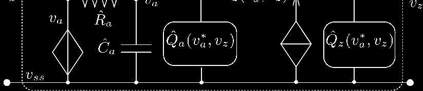
15 Waveform Independent Delay Models - CSM Model port currents as functions of port voltages At least one voltage controlled current source Additional components to model dynamic behaviour Capacitors Delay lines Charges Filters Usually one CSM per timing arc 15


16 Different CSM approaches Blade and Razor [Croix03] shape of output waveform Delay added d Error minimization CSM of Peng Li et. al. SPICE compatible Model parameters by error minimization Tuning of parameters 16


17 Different CSM approaches General Model [Amin06] Current and charges are functions of all port voltages Multiple input switching Internal nodes 17


18 Characterization Flows SPICE Logic Cell Transistor Netlist (SUBCKT) CSM Parameter Statistic Variation Topology Analysis Physical Reasoning More Information 18


19 Relation between Logic Cell and Current Source Model parasitic delay CSM DC port currents port charges lowpass filter (only for large gates) 19
20 DC-Transfer Characteristic Automaticaly derived from netlist DC simulation 20
21 Additional Dynamic Port Current Automatically derived from netlist DC simulation 21
22 Voltage Approximation Error for Large Inverter (input) 22


23 Characterization - cells with stacked transistors 23
24 Model each Channel Connected Block 24
25 Simulation for Buffer gate (parasitic layout) 25


26 Typical Lookup Tables for Model Components 26
27 Approximation of Lookup Tables Radial Base Functions [1] Splines Legendre Polynoms [Goel08] 27
28 Comparison of Static Output Current bilinear Interpolation, 50x50 grid, 100x100 for simulation 28
29 Model Implementation.SUBCKT R_SND3X015_A11_Z A B C Z VDD VSS LUT ZCHR_IN_A_Z A VSS Z VSS Z_CHARGE + params=(d_xl_thin=xl_thin D_XW_THIN=XW_THIN D_NDEP_NREG=NDEP_NREG) + MODLIB='CSM2' + file='r_snd3x015/zms/r_snd3x015_q_a_z_a10_z01_b1_c1' ZCUR_OUT_Z_A Z VSS A VSS Z_CURRENT + params=(d_xl_thin=xl_thin D_XW_THIN=XW_THIN D_NDEP_NREG=NDEP_NREG) + MODLIB='CSM2' + file='r_snd3x015/zms/r_snd3x015_i_z_a_a10_z01_b1_c1' ZCHR_OUT_Z_A Z VSS A VSS Z_CHARGE + params=(d_xl_thin=xl_thin D_XW_THIN=XW_THIN D_NDEP_NREG=NDEP_NREG) + MODLIB='CSM2' + file='r_snd3x015/zms/r_snd3x015_q_z_a_a10_z01_b1_c1'.ends VCCS: Compiled Models (C-Code) $tablemodel (Verilog-A) VC dynamic CS: C (constant capacitor) C(v) (voltage controlled capacitor) Compiled Models (C-Code) $tablemodel (Verilog-A) Data needed during Initialization Calculations during Newton Iteration Memory footprint (50x50, at least 3 tables) 29
30 CSM Implementation for SPICE Simulators.SUBCKT R_SND3X015_A11_Z A B C Z VDD VSS ZCHR_IN_A_Z A VSS Z VSS Z_CHARGE + MODLIB='CSM' + file='r_snd3x015/zms/r_snd3x015_q_a_z_a10_z01_b1_c1' ZCUR_OUT_Z_A Z Z VSS A VSS Z_CURRENT + MODLIB='CSM' + file='r_snd3x015/zms/r_snd3x015_i_z_a_a10_z01_b1_c1' ZCHR_OUT_Z_A Z Z VSS A VSS Z_CHARGE + MODLIB='CSM' + file='r_snd3x015/zms/r_snd3x015_q_z_a_a10_z01_b1_c1'.ends 30
31 Our experience Bilinear Interpolation is fine Bottleneck is Model-Simulator-Communication Nonlinear Charges also bilinear interpolation many might look good but others are nonlinear Derivativ matters! Best suited to long resistive interconnects This is very other models fail Dimensions Memory expensive 3D tables Speed X w.r.t. modern SPICE simulators 5-10X w.r.t. FastSPICE simulators 31
32 Summary on Current Source Models Very accurate delay models for logic cells Arbitrary loads and waveform -> SI, Timing, Noise In SPICE Simulators or special purpose simulators Naming ambiguity with EDA vendors Thank you for your attention 32
Amber Path FX SPICE Accurate Statistical Timing for 40nm and Below Traditional Sign-Off Wastes 20% of the Timing Margin at 40nm
 Amber Path FX SPICE Accurate Statistical Timing for 40nm and Below Amber Path FX is a trusted analysis solution for designers trying to close on power, performance, yield and area in 40 nanometer processes
Interconnect Delay Compensation in Timing Analysis for. Designs Containing Multiple Voltage Domains
 Interconnect Delay Compensation in Timing Analysis for Designs Containing Multiple oltage Domains Incentia Design Systems, Inc. 1. Introduction A timing signal may flow from one voltage domain to another
Current Based Delay Models: A Must For Nanometer Timing
 Current Based Delay Models: A Must For Nanometer Timing Ratnakar Goyal rgoyal@cadence.com Naresh Kumar nkumar@cadence.com Cadence Design Systems, Inc. Abstract In order to accurately account for nanometer
Mixed Signal Virtual Components COLINE, a case study
 Mixed Signal Virtual Components COLINE, a case study J.F. POLLET - DOLPHIN INTEGRATION Meylan - FRANCE http://www.dolphin.fr Overview of the presentation Introduction COLINE, an example of Mixed Signal
CMOS Digital Logic Design with Verilog. Chapter1 Digital IC Design &Technology
 CMOS Digital Logic Design with Verilog Chapter1 Digital IC Design &Technology Chapter Overview: In this chapter we study the concept of digital hardware design & technology. This chapter deals the standard
Lecture 4&5 CMOS Circuits
 Lecture 4&5 CMOS Circuits Xuan Silvia Zhang Washington University in St. Louis http://classes.engineering.wustl.edu/ese566/ Worst-Case V OL 2 3 Outline Combinational Logic (Delay Analysis) Sequential Circuits
Accurate Timing and Power Characterization of Static Single-Track Full-Buffers
 Accurate Timing and Power Characterization of Static Single-Track Full-Buffers By Rahul Rithe Department of Electronics & Electrical Communication Engineering Indian Institute of Technology Kharagpur,
THE SPICE BOOK. Andrei Vladimirescu. John Wiley & Sons, Inc. New York Chichester Brisbane Toronto Singapore
 THE SPICE BOOK Andrei Vladimirescu John Wiley & Sons, Inc. New York Chichester Brisbane Toronto Singapore CONTENTS Introduction SPICE THE THIRD DECADE 1 1.1 THE EARLY DAYS OF SPICE 1 1.2 SPICE IN THE 1970s
PHYSICAL STRUCTURE OF CMOS INTEGRATED CIRCUITS. Dr. Mohammed M. Farag
 PHYSICAL STRUCTURE OF CMOS INTEGRATED CIRCUITS Dr. Mohammed M. Farag Outline Integrated Circuit Layers MOSFETs CMOS Layers Designing FET Arrays EE 432 VLSI Modeling and Design 2 Integrated Circuit Layers
CharFlo-Cell! Cell! Next-Generation Solution for Characterizing and Modeling Standard Cell and I/O Library
 CharFlo-Cell! Cell! TM Next-Generation Solution for Characterizing and Modeling Standard Cell and I/O Library Agenda Introduction The Flow of CharFlo-Cell! The Applications and Features BiSection Methods
Power Estimation. Naehyuck Chang Dept. of EECS/CSE Seoul National University
 Power Estimation Naehyuck Chang Dept. of EECS/CSE Seoul National University naehyuck@snu.ac.kr 1 Contents Embedded Low-Power ELPL Laboratory SPICE power analysis Power estimation basics Signal probability
Substrate Level Noise Analysis Tool (SNAT) in Mixed Signal circuits
 in Mixed Signal circuits") Substrate Level Noise Analysis Tool (SNAT) in Mixed Signal circuits Anish joseph Research Scholar Abstract: There exist several tools that can be used to predict the substrate noise profile of digital
Substrate Level Noise Analysis Tool (SNAT) in Mixed Signal circuits Anish joseph Research Scholar Abstract: There exist several tools that can be used to predict the substrate noise profile of digital
CMOS VLSI Design (A3425)
") CMOS VLSI Design (A3425) Unit V Dynamic Logic Concept Circuits Contents Charge Leakage Charge Sharing The Dynamic RAM Cell Clocks and Synchronization Clocked-CMOS Clock Generation Circuits Communication
CMOS VLSI Design (A3425) Unit V Dynamic Logic Concept Circuits Contents Charge Leakage Charge Sharing The Dynamic RAM Cell Clocks and Synchronization Clocked-CMOS Clock Generation Circuits Communication
Mentor Analog Simulators
 ENGR-434 Spice Netlist Syntax Details Introduction Rev 5/25/11 As you may know, circuit simulators come in several types. They can be broadly grouped into those that simulate a circuit in an analog way,
UNIT-III POWER ESTIMATION AND ANALYSIS
 UNIT-III POWER ESTIMATION AND ANALYSIS In VLSI design implementation simulation software operating at various levels of design abstraction. In general simulation at a lower-level design abstraction offers
An Analog Phase-Locked Loop
 1 An Analog Phase-Locked Loop Greg Flewelling ABSTRACT This report discusses the design, simulation, and layout of an Analog Phase-Locked Loop (APLL). The circuit consists of five major parts: A differential
CS250 VLSI Systems Design. Lecture 3: Physical Realities: Beneath the Digital Abstraction, Part 1: Timing
 CS250 VLSI Systems Design Lecture 3: Physical Realities: Beneath the Digital Abstraction, Part 1: Timing Fall 2010 Krste Asanovic, John Wawrzynek with John Lazzaro and Yunsup Lee (TA) What do Computer
Accurate and Efficient Macromodel of Submicron Digital Standard Cells
 Accurate and Efficient Macromodel of Submicron Digital Standard Cells Cristiano Forzan, Bruno Franzini and Carlo Guardiani SGS-THOMSON Microelectronics, via C. Olivetti, 2, 241 Agrate Brianza (MI), ITALY
FDTD SPICE Analysis of High-Speed Cells in Silicon Integrated Circuits
 FDTD Analysis of High-Speed Cells in Silicon Integrated Circuits Neven Orhanovic and Norio Matsui Applied Simulation Technology Gateway Place, Suite 8 San Jose, CA 9 {neven, matsui}@apsimtech.com Abstract
2009 Spring CS211 Digital Systems & Lab 1 CHAPTER 3: TECHNOLOGY (PART 2)
") 1 CHAPTER 3: IMPLEMENTATION TECHNOLOGY (PART 2) Whatwillwelearninthischapter? we learn in this 2 How transistors operate and form simple switches CMOS logic gates IC technology FPGAs and other PLDs Basic
1 CHAPTER 3: IMPLEMENTATION TECHNOLOGY (PART 2) Whatwillwelearninthischapter? we learn in this 2 How transistors operate and form simple switches CMOS logic gates IC technology FPGAs and other PLDs Basic
Circuit Seed Overview
 Planting the Future of Electronic Designs Circuit Seed Overview Circuit Seed is family of inventions that work together to process analog signals using 100% digital parts. These are digital circuits and
Ramon Canal NCD Master MIRI. NCD Master MIRI 1
 Wattch, Hotspot, Hotleakage, McPAT http://www.eecs.harvard.edu/~dbrooks/wattch-form.html http://lava.cs.virginia.edu/hotspot http://lava.cs.virginia.edu/hotleakage http://www.hpl.hp.com/research/mcpat/
EE241 - Spring 2013 Advanced Digital Integrated Circuits. Projects. Groups of 3 Proposals in two weeks (2/20) Topics: Lecture 5: Transistor Models
 Topics: Lecture 5: Transistor Models") EE241 - Spring 2013 Advanced Digital Integrated Circuits Lecture 5: Transistor Models Projects Groups of 3 Proposals in two weeks (2/20) Topics: Soft errors in datapaths Soft errors in memory Integration
EE241 - Spring 2013 Advanced Digital Integrated Circuits Lecture 5: Transistor Models Projects Groups of 3 Proposals in two weeks (2/20) Topics: Soft errors in datapaths Soft errors in memory Integration
Low Power Design Methods: Design Flows and Kits
 JOINT ADVANCED STUDENT SCHOOL 2011, Moscow Low Power Design Methods: Design Flows and Kits Reported by Shushanik Karapetyan Synopsys Armenia Educational Department State Engineering University of Armenia
ELEC Digital Logic Circuits Fall 2015 Delay and Power
 ELEC - Digital Logic Circuits Fall 5 Delay and Power Vishwani D. Agrawal James J. Danaher Professor Department of Electrical and Computer Engineering Auburn University, Auburn, AL 36849 http://www.eng.auburn.edu/~vagrawal
EDA Challenges for Low Power Design. Anand Iyer, Cadence Design Systems
 EDA Challenges for Low Power Design Anand Iyer, Cadence Design Systems Agenda Introduction ti LP techniques in detail Challenges to low power techniques Guidelines for choosing various techniques Why is
Jack Keil Wolf Lecture. ESE 570: Digital Integrated Circuits and VLSI Fundamentals. Lecture Outline. MOSFET N-Type, P-Type.
 ESE 570: Digital Integrated Circuits and VLSI Fundamentals Jack Keil Wolf Lecture Lec 3: January 24, 2019 MOS Fabrication pt. 2: Design Rules and Layout http://www.ese.upenn.edu/about-ese/events/wolf.php
3-2-1 Contact: An Experimental Approach to the Analysis of Contacts in 45 nm and Below. Rasit Onur Topaloglu, Ph.D.
 3-2-1 Contact: An Experimental Approach to the Analysis of Contacts in 45 nm and Below Rasit Onur Topaloglu, Ph.D. Outline Introduction and Motivation Impact of Contact Resistance Test Structures for Contact
Evaluation of Package Properties for RF BJTs
 Application Note Evaluation of Package Properties for RF BJTs Overview EDA simulation software streamlines the development of digital and analog circuits from definition of concept and estimation of required
Transistor Digital Circuits
 Recapitulation Transistor Digital Circuits The transistor Operating principle and regions Utilization of the transistor Transfer characteristics, symbols Controlled switch model BJT digital circuits MOSFET
Appendix. RF Transient Simulator. Page 1
 Appendix RF Transient Simulator Page 1 RF Transient/Convolution Simulation This simulator can be used to solve problems associated with circuit simulation, when the signal and waveforms involved are modulated
ECE 471/571 The CMOS Inverter Lecture-6. Gurjeet Singh
 ECE 471/571 The CMOS Inverter Lecture-6 Gurjeet Singh NMOS-to-PMOS ratio,pmos are made β times larger than NMOS Sizing Inverters for Performance Conclusions: Intrinsic delay tp0 is independent of sizing
Andrew Clinton, Matt Liberty, Ian Kuon
 Andrew Clinton, Matt Liberty, Ian Kuon FPGA Routing (Interconnect) FPGA routing consists of a network of wires and programmable switches Wire is modeled with a reduced RC network Drivers are modeled as
Dr. Ralf Sommer. Munich, March 8th, 2006 COM BTS DAT DF AMF. Presenter Dept Titel presentation Date Page 1
 DATE 2006 Special Session: DFM/DFY Design for Manufacturability and Yield - Influence of Process Variations in Digital, Analog and Mixed-Signal Circuit Design DATE 06 Munich, March 8th, 2006 Presenter
ESE 570: Digital Integrated Circuits and VLSI Fundamentals
 ESE 570: Digital Integrated Circuits and VLSI Fundamentals Lec 3: January 24, 2019 MOS Fabrication pt. 2: Design Rules and Layout Penn ESE 570 Spring 2019 Khanna Jack Keil Wolf Lecture http://www.ese.upenn.edu/about-ese/events/wolf.php
! Review: MOS IV Curves and Switch Model. ! MOS Device Layout. ! Inverter Layout. ! Gate Layout and Stick Diagrams. ! Design Rules. !
 ESE 570: Digital Integrated Circuits and VLSI Fundamentals Lec 3: January 21, 2016 MOS Fabrication pt. 2: Design Rules and Layout Lecture Outline! Review: MOS IV Curves and Switch Model! MOS Device Layout!
ESE 570: Digital Integrated Circuits and VLSI Fundamentals
 ESE 570: Digital Integrated Circuits and VLSI Fundamentals Lec 3: January 21, 2016 MOS Fabrication pt. 2: Design Rules and Layout Penn ESE 570 Spring 2016 Khanna Adapted from GATech ESE3060 Slides Lecture
Engr354: Digital Logic Circuits
 Engr354: Digital Logic Circuits Chapter 3: Implementation Technology Curtis Nelson Chapter 3 Overview In this chapter you will learn about: How transistors are used as switches; Integrated circuit technology;
DATASHEET CADENCE QRC EXTRACTION
 DATASHEET Cadence QRC Etraction, the industry s premier 3D fullchip parasitic etractor that is independent of design style or flow, is a fast and accurate RLCK etraction solution used during design implementation
Lecture 10. Circuit Pitfalls
 Lecture 10 Circuit Pitfalls Intel Corporation jstinson@stanford.edu 1 Overview Reading Lev Signal and Power Network Integrity Chandrakasen Chapter 7 (Logic Families) and Chapter 8 (Dynamic logic) Gronowski
FinFET SPICE Modeling
 FinFET SPICE Modeling Synopsys Solutions to Simulation Challenges of Advanced Technology Nodes Joddy Wang December 9, 2015 Outline SPICE Model for IC Design FinFET Modeling Challenges Solutions Summary
Microelectronics, BSc course
 Microelectronics, BSc course MOS circuits: CMOS circuits, construction http://www.eet.bme.hu/~poppe/miel/en/14-cmos.pptx http://www.eet.bme.hu The abstraction level of our study: SYSTEM + MODULE GATE CIRCUIT
Analog-aware Schematic Synthesis
 12 Analog-aware Schematic Synthesis Yuping Wu Institute of Microelectronics, Chinese Academy of Sciences, China 1. Introduction An analog circuit has great requirements of constraints on circuit and layout
RECENT technology trends have lead to an increase in
 IEEE JOURNAL OF SOLID-STATE CIRCUITS, VOL. 39, NO. 9, SEPTEMBER 2004 1581 Noise Analysis Methodology for Partially Depleted SOI Circuits Mini Nanua and David Blaauw Abstract In partially depleted silicon-on-insulator
A Current-based Method for Short Circuit Power Calculation under Noisy Input Waveforms *
 A Current-based Method for Short Circuit Power Calculation under Noisy Input Waveforms * Hanif Fatemi Shahin Nazarian Massoud Pedram EE-Systems Dept., University of Southern California Los Angeles, CA
The Physical Design of Long Time Delay-chip
 2011 International Conference on Computer Science and Information Technology (ICCSIT 2011) IPCSIT vol. 51 (2012) (2012) IACSIT Press, Singapore DOI: 10.7763/IPCSIT.2012.V51.137 The Physical Design of Long
! Review: MOS IV Curves and Switch Model. ! MOS Device Layout. ! Inverter Layout. ! Gate Layout and Stick Diagrams. ! Design Rules. !
 ESE 570: Digital Integrated Circuits and VLSI Fundamentals Lec 3: January 21, 2017 MOS Fabrication pt. 2: Design Rules and Layout Lecture Outline! Review: MOS IV Curves and Switch Model! MOS Device Layout!
! MOS Device Layout. ! Inverter Layout. ! Gate Layout and Stick Diagrams. ! Design Rules. ! Standard Cells. ! CMOS Process Enhancements
 EE 570: igital Integrated Circuits and VLI Fundamentals Lec 3: January 18, 2018 MO Fabrication pt. 2: esign Rules and Layout Lecture Outline! MO evice Layout! Inverter Layout! Gate Layout and tick iagrams!
Simulation using Tutorial Verilog XL Release Date: 02/12/2005
 Simulation using Tutorial - 1 - Logic Simulation using Verilog XL: This tutorial includes one way of simulating digital circuits using Verilog XL. Here we have taken an example of two cascaded inverters.
Introduction to Digital VLSI Design מבוא לתכנון VLSI ספרתי
 Design מבוא לתכנון VLSI ספרתי Extraction Lecturer: Gil Rahav Semester B, EE Dept. BGU. Freescale Semiconductors Israel Slide 1 Extraction Extraction is a process of creating electrical representation (R&C)
Ansoft Designer with Nexxim. Statistical Eye Capabilities
 Ansoft Designer with Nexxim Statistical Eye Capabilities Problem Statement Load Generic 0.25um M odels Buffer PCIE Connector BYPASS Planar EM S S S TRL TRL TRL TRL TRL TRL Programmable W-Element SI Wave
On Chip Active Decoupling Capacitors for Supply Noise Reduction for Power Gating and Dynamic Dual Vdd Circuits in Digital VLSI
 ELEN 689 606 Techniques for Layout Synthesis and Simulation in EDA Project Report On Chip Active Decoupling Capacitors for Supply Noise Reduction for Power Gating and Dynamic Dual Vdd Circuits in Digital
Analog Technology Forum 2008
 Single Vendor Design Flow Solutions for Low Power Electronics Analog Technology Forum 2008 Dr. Ivan Pesic June 25 2008 Simucad 社製品販売サポート Pressure Points on EDA Vendors for Continuous Improvements To be
Experiences and Benefits of 16nm and 10nm FinFET Development
 Experiences and Benefits of 16nm and 10nm FinFET Development Jeff Galloway, Paweł Banachowicz, Michael Kroger, Brian Eplett, Andrew Cole, Randy Caplan Silicon Creations Process Experience Silicon Creations
Behavioural Modeling and Simulation of a Switched-Current Phase Locked Loop
 Behavioural Modeling and Simulation of a Switched-Current Phase Locked Loop Peter R. Wilson, Reuben Wilcock, Bashir Al-Hashimi & Andrew D. Brown Electronic Systems Design Group prw@ecs.soton.ac.uk 1 Introduction
EE E6930 Advanced Digital Integrated Circuits. Spring, 2002 Lecture 7. Clocked and self-resetting logic I
 EE E6930 Advanced Digital Integrated Circuits Spring, 2002 Lecture 7. Clocked and self-resetting logic I References CBF, Chapter 8 DP, Section 4.3.3.1-4.3.3.4 Bernstein, High-speed CMOS design styles,
PROCESS-VOLTAGE-TEMPERATURE (PVT) VARIATIONS AND STATIC TIMING ANALYSIS
 VARIATIONS AND STATIC TIMING ANALYSIS") PROCESS-VOLTAGE-TEMPERATURE (PVT) VARIATIONS AND STATIC TIMING ANALYSIS The major design challenges of ASIC design consist of microscopic issues and macroscopic issues [1]. The microscopic issues are ultra-high
PROCESS-VOLTAGE-TEMPERATURE (PVT) VARIATIONS AND STATIC TIMING ANALYSIS The major design challenges of ASIC design consist of microscopic issues and macroscopic issues [1]. The microscopic issues are ultra-high
Ramya Srinivasan GLOBALFOUNDRIES 22FDX: Tempus Body-Bias Interpolation QoR. April
 Ramya Srinivasan GLOBALFOUNDRIES 22FDX: Tempus Body-Bias Interpolation QoR April 12 2017 22FDX: Tempus Body-Bias Interpolation QoR Presenter: Ramya Srinivasan Authors GLOBALFOUNDRIES: Haritez Narisetty
The backend duplication method
 The backend duplication method - A Leakage-Proof Place-and and-route Strategy for Secured ASICs - CHES Workshop August 30th September 1st 2005 Edinburgh, Scotland, UK. Sylvain GUILLEY (*), Philippe HOOGVORST
Intelligent Systems Group Department of Electronics. An Evolvable, Field-Programmable Full Custom Analogue Transistor Array (FPTA)
") Department of Electronics n Evolvable, Field-Programmable Full Custom nalogue Transistor rray (FPT) Outline What`s Behind nalog? Evolution Substrate custom made configurable transistor array (FPT) Ways
Department of Electronics n Evolvable, Field-Programmable Full Custom nalogue Transistor rray (FPT) Outline What`s Behind nalog? Evolution Substrate custom made configurable transistor array (FPT) Ways
Minimizing Spurious Switching Activities With Transistor Sizing
 Minimizing Spurious Switching Activities With Transistor Sizing Artur Wróblewski Munich University of Technology Arcisstr. 1, 80333 München, Germany e mail: arwr@nws.e-technik.tu-muenchen.de Christian
Timing analysis can be done right after synthesis. But it can only be accurately done when layout is available
 Timing Analysis Lecture 9 ECE 156A-B 1 General Timing analysis can be done right after synthesis But it can only be accurately done when layout is available Timing analysis at an early stage is not accurate
Announcements. Advanced Digital Integrated Circuits. Project proposals due today. Homework 1. Lecture 8: Gate delays,
 EE4 - Spring 008 Advanced Digital Integrated Circuits Lecture 8: Gate delays, Variability Announcements Project proposals due today Title Team members ½ page ~5 references Post it on your EECS web page
VLSI Designed Low Power Based DPDT Switch
 International Journal of Electronics and Communication Engineering. ISSN 0974-2166 Volume 8, Number 1 (2015), pp. 81-86 International Research Publication House http://www.irphouse.com VLSI Designed Low
Introduction. Timing Verification
 Timing Verification Sungho Kang Yonsei University YONSEI UNIVERSITY Outline Introduction Timing Simulation Static Timing Verification PITA Conclusion 2 1 Introduction Introduction Variations in component
Worst-Case Aggressor-Victim Alignment with Current-Source Driver Models
 3.1 Worst-Case Aggressor-Victim Alignment with Current-Source Driver Models Ravikishore Gandikota University of Michigan Li Ding Synopsys, CA David Blaauw University of Michigan Peivand Tehrani Synopsys,
A Self-Contained Large-Scale FPAA Development Platform
 A SelfContained LargeScale FPAA Development Platform Christopher M. Twigg, Paul E. Hasler, Faik Baskaya School of Electrical and Computer Engineering Georgia Institute of Technology, Atlanta, Georgia 303320250
IC Layout Design of 4-bit Universal Shift Register using Electric VLSI Design System
 IC Layout Design of 4-bit Universal Shift Register using Electric VLSI Design System 1 Raj Kumar Mistri, 2 Rahul Ranjan, 1,2 Assistant Professor, RTC Institute of Technology, Anandi, Ranchi, Jharkhand,
30 ma flash LDO voltage regulator (output voltage 1.8 ± 0.2 V)
") SPECIFICATION 1 FEATURES Global Foundries CMOS 55 nm Low drop out Low current consumption Two modes operations: Normal, Economy Mode operation Bypass No discrete filtering capacitors required (cap-less
SPECIFICATION 1 FEATURES Global Foundries CMOS 55 nm Low drop out Low current consumption Two modes operations: Normal, Economy Mode operation Bypass No discrete filtering capacitors required (cap-less
ECEN 474/704 Lab 5: Frequency Response of Inverting Amplifiers
 ECEN 474/704 Lab 5: Frequency Response of Inverting Amplifiers Objective Design, simulate and layout various inverting amplifiers. Introduction Inverting amplifiers are fundamental building blocks of electronic
DesignCon On-Chip Power Supply Noise and Reliability Analysis for Multi-Gigabit I/O Interfaces
 DesignCon 2010 On-Chip Power Supply Noise and Reliability Analysis for Multi-Gigabit I/O Interfaces Ralf Schmitt, Rambus Inc. [Email: rschmitt@rambus.com] Hai Lan, Rambus Inc. Ling Yang, Rambus Inc. Abstract
ECE321 Electronics I Fall 2006
 ECE321 Electronics I Fall 2006 Professor James E. Morris Lecture 1 25 th September, 2006 PowerPoint Overheads for Sedra/Smith Microelectronic Circuits 5/e 2004 Oxford University Press. 1 Oxford University
ECE 521. Design Flow. Fall 2016 Simulation. Design Verification. Why Solve Equations on a Computer?
 Design Flow Comparison with specs Redesign Concept Implementation Design Specifications Circuit Schematic ECE 521 Layout SPICE etc. Physical definition Fall 2016 Physical verification Parasitic Extraction
A CMOS CURRENT CONTROLLED RING OSCILLATOR WITH WIDE AND LINEAR TUNING RANGE
 A CMOS CURRENT CONTROLLED RING OSCILLATOR WI WIDE AND LINEAR TUNING RANGE Abstract Ekachai Leelarasmee 1 1 Electrical Engineering Department, Chulalongkorn University, Bangkok 10330, Thailand Tel./Fax.
A Review of Phase Locked Loop Design Using VLSI Technology for Wireless Communication.
 A Review of Phase Locked Loop Design Using VLSI Technology for Wireless Communication. PG student, M.E. (VLSI and Embedded system) G.H.Raisoni College of Engineering and Management, A nagar Abstract: The
Static Random Access Memory - SRAM Dr. Lynn Fuller Webpage:
 ROCHESTER INSTITUTE OF TECHNOLOGY MICROELECTRONIC ENGINEERING Static Random Access Memory - SRAM Dr. Lynn Fuller Webpage: http://people.rit.edu/lffeee 82 Lomb Memorial Drive Rochester, NY 14623-5604 Email:
The Design and Characterization of an 8-bit ADC for 250 o C Operation
 The Design and Characterization of an 8-bit ADC for 25 o C Operation By Lynn Reed, John Hoenig and Vema Reddy Tekmos, Inc. 791 E. Riverside Drive, Bldg. 2, Suite 15, Austin, TX 78744 Abstract Many high
MDLL & Slave Delay Line performance analysis using novel delay modeling
 MDLL & Slave Delay Line performance analysis using novel delay modeling Abhijith Kashyap, Avinash S and Kalpesh Shah Backplane IP division, Texas Instruments, Bangalore, India E-mail : abhijith.r.kashyap@ti.com
ELEC451 Integrated Circuit Engineering Fall 2009 Solution to CAD Assignment 2 Inverter Voltage Transfer Characteristic (VTC)
") ELEC451 Integrated Circuit Engineering Fall 2009 Solution to CAD Assignment 2 Inverter Voltage Transfer Characteristic (VTC) The plot below shows how the inverter's threshold voltage changes with the relative
ELEC451 Integrated Circuit Engineering Fall 2009 Solution to CAD Assignment 2 Inverter Voltage Transfer Characteristic (VTC) The plot below shows how the inverter's threshold voltage changes with the relative
Advanced Techniques for Using ARM's Power Management Kit
 ARM Connected Community Technical Symposium Advanced Techniques for Using ARM's Power Management Kit Libo Chang( 常骊波 ) ARM China 2006 年 12 月 4/6/8 日, 上海 / 北京 / 深圳 Power is Out of Control! Up to 90nm redu
A New and Accurate Interconnection Delay Time Evaluation in a general Tree Type Network.
 A New and Accurate Interconnection Delay Time Evaluation in a general Tree Type Network. D. DESCHACHT, C. DABRIN Laboratoire d Informatique, de Robotique et de Microélectronique UMR CNRS 998 Université
Noise Constraint Driven Placement for Mixed Signal Designs. William Kao and Wenkung Chu October 20, 2003 CAS IEEE SCV Meeting
 Noise Constraint Driven Placement for Mixed Signal Designs William Kao and Wenkung Chu October 20, 2003 CAS IEEE SCV Meeting Introduction OUTLINE Substrate Noise: Some Background Substrate Noise Network
Towards PVT-Tolerant Glitch-Free Operation in FPGAs
 Towards PVT-Tolerant Glitch-Free Operation in FPGAs Safeen Huda and Jason H. Anderson ECE Department, University of Toronto, Canada 24 th ACM/SIGDA International Symposium on FPGAs February 22, 2016 Motivation
Characterization and Variation Modeling for 22FDX. Ning Jin Digital Design Methodology Team
 Characterization and Variation Modeling for 22FDX Ning Jin Digital Design Methodology Team Agenda 1 2 3 4 Introduction to 22FDX Technology Library Characterization in Liberate and Variety Library Characterization
A Practical Approach to Obtain Defect Matrix for Integrated Circuit Testing
 A Practical Approach to Obtain Defect Matrix for Integrated Circuit Testing LARISSA SOARES Federal University of Paraíba Department of Electrical Engineering Cidade Universitária, n/n João Pessoa BRAZIL
Digital Integrated Circuits Designing Combinational Logic Circuits. Fuyuzhuo
 Digital Integrated Circuits Designing Combinational Logic Circuits Fuyuzhuo Introduction Digital IC Combinational vs. Sequential Logic In Combinational Logic Circuit Out In Combinational Logic Circuit
Using GoldenGate to Verify and Improve Your Designs Using Real Signals
 Using GoldenGate to Verify and Improve Your Designs Using Real Signals Enabling more complete understanding of your designs Agilent EEsof EDA 1 Outline What problems do designers face? Main point of this
Fixing Antenna Problem by Dynamic Diode Dropping and Jumper Insertion
 Fixing Antenna Problem by Dynamic Dropping and Jumper Insertion Peter H. Chen and Sunil Malkani Chun-Mou Peng James Lin TeraLogic, Inc. International Tech. Univ. National Semi. Corp. 1240 Villa Street
Methodology for Circuit Optimization
 Methodology for Circuit Optimization by KENDRA L. MARKLE Submitted to the Department of Electrical Engineering and Computer Science in partial fulfillment of the requirements for the degree of Bachelor
43.2. Figure 1. Interconnect analysis using linear simulation and superposition
 43.2 Driver Modeling and Alignment for Worst-Case Delay Noise Supamas Sirichotiyakul, David Blaauw, Chanhee Oh, Rafi Levy*, Vladimir Zolotov, Jingyan Zuo Motorola Inc. Austin, TX, *Motorola Semiconductor
INF4420. Outline. Switched capacitor circuits. Switched capacitor introduction. MOSFET as an analog switch 1 / 26 2 / 26.
 INF4420 Switched capacitor circuits Spring 2012 Jørgen Andreas Michaelsen (jorgenam@ifi.uil.no) 1 / 26 Outline Switched capacitor introduction MOSFET as an analog switch 2 / 26 Introduction Discrete time
Design of Low Power CMOS Startup Charge Pump Based on Body Biasing Technique
 Design of Low Power CMOS Startup Charge Pump Based on Body Biasing Technique Juliet Abraham 1, Dr. B. Paulchamy 2 1 PG Scholar, Hindusthan institute of Technology, coimbtore-32, India 2 Professor and HOD,
Homework 10 posted just for practice. Office hours next week, schedule TBD. HKN review today. Your feedback is important!
 EE141 Fall 2005 Lecture 26 Memory (Cont.) Perspectives Administrative Stuff Homework 10 posted just for practice No need to turn in Office hours next week, schedule TBD. HKN review today. Your feedback
PROGRAMMABLE ASIC INTERCONNECT
 PROGRAMMABLE ASIC INTERCONNECT The structure and complexity of the interconnect is largely determined by the programming technology and the architecture of the basic logic cell The first programmable ASICs
DIGITAL INTEGRATED CIRCUITS A DESIGN PERSPECTIVE 2 N D E D I T I O N
 DIGITAL INTEGRATED CIRCUITS A DESIGN PERSPECTIVE 2 N D E D I T I O N Jan M. Rabaey, Anantha Chandrakasan, and Borivoje Nikolic CONTENTS PART I: THE FABRICS Chapter 1: Introduction (32 pages) 1.1 A Historical
NanoFabrics: : Spatial Computing Using Molecular Electronics
 NanoFabrics: : Spatial Computing Using Molecular Electronics Seth Copen Goldstein and Mihai Budiu Computer Architecture, 2001. Proceedings. 28th Annual International Symposium on 30 June-4 4 July 2001
Logic Synthesis. Logic synthesis transforms RTL code into a gate-level netlist. RTL Verilog converted into Structural Verilog
 Logic Synthesis Logic synthesis transforms RTL code into a gate-level netlist RTL Verilog converted into Structural Verilog Logic Synthesis - The process and steps Translation Check RTL for valid syntax
Preface to Third Edition Deep Submicron Digital IC Design p. 1 Introduction p. 1 Brief History of IC Industry p. 3 Review of Digital Logic Gate
 Preface to Third Edition p. xiii Deep Submicron Digital IC Design p. 1 Introduction p. 1 Brief History of IC Industry p. 3 Review of Digital Logic Gate Design p. 6 Basic Logic Functions p. 6 Implementation
EECS150 - Digital Design Lecture 15 - CMOS Implementation Technologies. Overview of Physical Implementations
 EECS150 - Digital Design Lecture 15 - CMOS Implementation Technologies Mar 12, 2013 John Wawrzynek Spring 2013 EECS150 - Lec15-CMOS Page 1 Overview of Physical Implementations Integrated Circuits (ICs)
EECS150 - Digital Design Lecture 9 - CMOS Implementation Technologies
 EECS150 - Digital Design Lecture 9 - CMOS Implementation Technologies Feb 14, 2012 John Wawrzynek Spring 2012 EECS150 - Lec09-CMOS Page 1 Overview of Physical Implementations Integrated Circuits (ICs)