電子回路論第 7 回 Electric Circuits for Physicists
|
|
|
- Cameron Wilson
- 5 years ago
- Views:
Transcription
1 電子回路論第 7 回 Electric Circuits for Physicists 東京大学理学部 理学系研究科物性研究所勝本信吾 Shingo Katsumoto
2 Outline 4.5 Field Effect Transistors (FETs) Ch.5 Distributed constant circuits 5.1 Transmission lines Coaxial cables Lecher lines Micro-strip lines 5.2 Wave propagation through transmission lines Connection and termination of transmission lines

3 Combination of an OP-amp and discrete transistors 10m 10k a Complementary push-pull V + R i R f 10k a 10m v in R in - R f + v out v in R in J in = J v out V R i Inversion amplifier Voltage, current booster
4 Depletion layer width with reverse bias voltage V bi + V Poisson equation p w p w n n

5 Effective capacitance and reverse bias voltage Doping profiler V bi V Varicap diode KB505 Frequency modulation Phase lock loop
 Junction FET (JFET)")

6 4.4 Field effect transistor (FET) Junction FET (JFET) Circuit symbols D D G G S S n-channel p-channel Pinch-off
7 Static characteristics of FET Ohmic area Space charge limited area
8 Space-charge limitation of source-drain current L G p+ w d (y) S n -N D e p+ V ch (y) G 2w t V g D y conductivity electric field channel width pinch off (internal) voltage: Only valid for w d < w t /2.
9 Static characteristics of FET transconductance Low bias current: small power consumption Drain resistance Locally linear approximation Amplification factor (voltage gain)
10 Biasing circuits for FETs Fixed bias circuit R 1 R D V DD V DD J D J D R D V GS R 2 Self-biasing circuit V DD V DS Generally more stable R D V DD V DD R D + R S J D J D V GS R 2 V GS R S V GS V DD V DS

11 Equivalent signal circuits for FET G S D Source grounded Drain grounded Gate grounded v i - + μv i r d v i + - μv i 1 + μ r d 1 + μ v i - + μv i r d
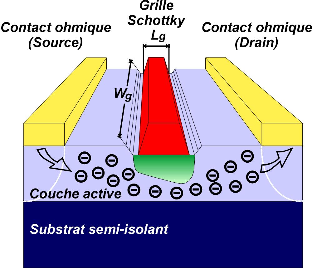


12 MES-FET


13 MOS-FET enhancement Simplified CMOS inverter circuit depletion Low leakage current Single gate input both on/off switch inversion
.")
14 MOSFET switching characteristics From datasheet CSD87381P power MOSFET (Texas instr.). More than 7 orders change in J D within 3 V change of V GS.
15 Ch.5 Distributed constant circuits Submarine cable map
16 Distributed constant circuit concept 1. In what case we need to consider distributed constant circuits? Characteristic sizes of devices wavelength of electromagnetic signal 2. A typical scheme to make the shift for distributed circuit Lumped constant circuit 1. Connection of unit circuits 2. Taking the infinitesimal limit Distributed constant circuit 3. Distributed constant circuits : transmission lines Coaxial cables, Lecher lines, micro-strip lines, waveguides, optical fibers


17 5.1.1 Coaxial cable Thin coaxial cable AWG50 (f25mm)

18 Transmission line as a series of infinitesimal terminal-pairs Transmission line divide into four terminal circuits Each unit should have delay. Ignore energy dissipation. L L L L L L C C C C C C Oliver Heaviside Then take the infinitesimal limit dx J J + dj Zdx Width 0, Number V Ydx V + dv Telegraphic equation

19 Characteristic impedance (dimension: L 1 ) -: Progressive, +: Retrograde Characteristic impedance Pure reactance Y = iωc, Z = iωl For L and C model (dimension: velocity)
20 Coaxial cable setup b r a e, m
21 Maxwell theory a b From Maxwell equations y z x However in TEM (transverse electric and magnetic) mode: i.e., the RHSs are zero. For the fields along x and y to survive, Propagation velocity In such a case, from Maxwell equations: Potentials are conceivable for H and E.

, the equivalence is")
22 Maxwell theory Cauchy-Riemann theorem Characteristic impedance: If we can express V and J in the form of distributed constant circuit model (L and C model), the equivalence is certified. Capacitance part
23 Maxwell theory Inductance part Core current J, shield current J Flux per length: Self inductance per length: cf. Characteristic impedance of vacuum

24 Coaxial cable 2
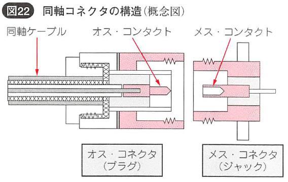

25 Coaxial connectors
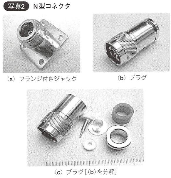

26 Coaxial connectors


27 Coaxial connectors 2 SMA-type jack plug K-type V-type


28 LEMO cables and connectors High-energy physics experiment, etc.

29 Lecher line
 strip Narrow (W/h<3.")
30 Micro strip line Wide (W/h>3.3) strip Narrow (W/h<3.3) strip
31 Connection and termination Z 0 Z 1 -l 0 x
32 Connection and termination J = J + + J (definition right positive) At x = 0: progressive retrograde V = V + + V = Z 0 J + J Reflection coefficient: Z 1 = Z 0 : no reflection, i.e., impedance matching Z 1 = + (open circuit end) : r = 1, i.e., free end Z 1 = 0 (short circuit end) : r = 1, i.e., fixed end
33 Connection and termination Finite reflection Standing wave Voltage-Standing Wave Ratio (VSWR): At x = - l Reflection coefficient:
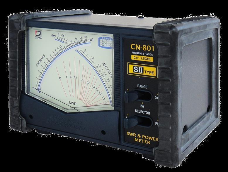


34 SWR measurement SWR Meters: Desktop types Cross-meter Handy type
35 Connection and termination Z 0 Z 1 -l 0 x
36 Connection and termination Transmission line connection. Characteristic impedance Z 0, Z 0 At the connection point, only the local relation between V and J affects the reflection coefficient. The local impedance from the left hand side is Z 0.
電子回路論第 7 回 Electric Circuits for Physicists #7
 電子回路論第 7 回 Electric Circuits for Physicists #7 東京大学理学部 理学系研究科物性研究所勝本信吾 Shingo Katsumoto Outline 4.5 Field Effect Transistors (FETs) Ch.5 Distributed constant circuits 5.1 Transmission lines 5.1.1 Coaxial
電子回路論第 6 回 Electric Circuits for Physicists
 電子回路論第 6 回 Electric Circuits for Physicists 東京大学理学部 理学系研究科物性研究所勝本信吾 Shingo Katsumoto Outline 4.3 Feedback control 4.3.1 Disturbance and noise 4.3.2 PID control 4.4 PN junction transistors 4.4.1 Diodes
IENGINEERS-CONSULTANTS QUESTION BANK SERIES ELECTRONICS ENGINEERING 1 YEAR UPTU ELECTRONICS ENGINEERING EC 101 UNIT 3 (JFET AND MOSFET)
") ELECTRONICS ENGINEERING EC 101 UNIT 3 (JFET AND MOSFET) LONG QUESTIONS (10 MARKS) 1. Draw the construction diagram and explain the working of P-Channel JFET. Also draw the characteristics curve and transfer
ELECTRONICS ENGINEERING EC 101 UNIT 3 (JFET AND MOSFET) LONG QUESTIONS (10 MARKS) 1. Draw the construction diagram and explain the working of P-Channel JFET. Also draw the characteristics curve and transfer
Field Effect Transistors (npn)
") Field Effect Transistors (npn) gate drain source FET 3 terminal device channel e - current from source to drain controlled by the electric field generated by the gate base collector emitter BJT 3 terminal
Field Effect Transistors (npn) gate drain source FET 3 terminal device channel e - current from source to drain controlled by the electric field generated by the gate base collector emitter BJT 3 terminal
FET(Field Effect Transistor)
") Field Effect Transistor: Construction and Characteristic of JFETs. Transfer Characteristic. CS,CD,CG amplifier and analysis of CS amplifier MOSFET (Depletion and Enhancement) Type, Transfer Characteristic,
Field Effect Transistor: Construction and Characteristic of JFETs. Transfer Characteristic. CS,CD,CG amplifier and analysis of CS amplifier MOSFET (Depletion and Enhancement) Type, Transfer Characteristic,
Three Terminal Devices
 Three Terminal Devices - field effect transistor (FET) - bipolar junction transistor (BJT) - foundation on which modern electronics is built - active devices - devices described completely by considering
Depletion-mode operation ( 공핍형 ): Using an input gate voltage to effectively decrease the channel size of an FET
: Using an input gate voltage to effectively decrease the channel size of an FET") Ch. 13 MOSFET Metal-Oxide-Semiconductor Field-Effect Transistor : I D D-mode E-mode V g The gate oxide is made of dielectric SiO 2 with e = 3.9 Depletion-mode operation ( 공핍형 ): Using an input gate voltage
Ch. 13 MOSFET Metal-Oxide-Semiconductor Field-Effect Transistor : I D D-mode E-mode V g The gate oxide is made of dielectric SiO 2 with e = 3.9 Depletion-mode operation ( 공핍형 ): Using an input gate voltage
Metal-Oxide-Silicon (MOS) devices PMOS. n-type
 devices PMOS. n-type") Metal-Oxide-Silicon (MOS devices Principle of MOS Field Effect Transistor transistor operation Metal (poly gate on oxide between source and drain Source and drain implants of opposite type to substrate.
Metal-Oxide-Silicon (MOS devices Principle of MOS Field Effect Transistor transistor operation Metal (poly gate on oxide between source and drain Source and drain implants of opposite type to substrate.
Radio Frequency Electronics
 Radio Frequency Electronics Active Components II Harry Nyquist Born in 1889 in Sweden Received B.S. and M.S. from U. North Dakota Received Ph.D. from Yale Worked and Bell Laboratories for all of his career
UNIT-VI FIELD EFFECT TRANSISTOR. 1. Explain about the Field Effect Transistor and also mention types of FET s.
 UNIT-I FIELD EFFECT TRANSISTOR 1. Explain about the Field Effect Transistor and also mention types of FET s. The Field Effect Transistor, or simply FET however, uses the voltage that is applied to their
(a) Current-controlled and (b) voltage-controlled amplifiers.
 Current-controlled and (b) voltage-controlled amplifiers.") Fig. 6.1 (a) Current-controlled and (b) voltage-controlled amplifiers. Fig. 6.2 Drs. Ian Munro Ross (front) and G. C. Dacey jointly developed an experimental procedure for measuring the characteristics
Fig. 6.1 (a) Current-controlled and (b) voltage-controlled amplifiers. Fig. 6.2 Drs. Ian Munro Ross (front) and G. C. Dacey jointly developed an experimental procedure for measuring the characteristics
Unit III FET and its Applications. 2 Marks Questions and Answers
 Unit III FET and its Applications 2 Marks Questions and Answers 1. Why do you call FET as field effect transistor? The name field effect is derived from the fact that the current is controlled by an electric
KOM2751 Analog Electronics :: Dr. Muharrem Mercimek :: YTU - Control and Automation Dept. 1 6 FIELD-EFFECT TRANSISTORS
 KOM2751 Analog Electronics :: Dr. Muharrem Mercimek :: YTU - Control and Automation Dept. 1 6 FIELD-EFFECT TRANSISTORS Most of the content is from the textbook: Electronic devices and circuit theory, Robert
ECE 340 Lecture 40 : MOSFET I
 ECE 340 Lecture 40 : MOSFET I Class Outline: MOS Capacitance-Voltage Analysis MOSFET - Output Characteristics MOSFET - Transfer Characteristics Things you should know when you leave Key Questions How do
Gechstudentszone.wordpress.com
 UNIT 4: Small Signal Analysis of Amplifiers 4.1 Basic FET Amplifiers In the last chapter, we described the operation of the FET, in particular the MOSFET, and analyzed and designed the dc response of circuits
Lecture 3: Transistors
 Lecture 3: Transistors Now that we know about diodes, let s put two of them together, as follows: collector base emitter n p n moderately doped lightly doped, and very thin heavily doped At first glance,
6. Field-Effect Transistor
 6. Outline: Introduction to three types of FET: JFET MOSFET & CMOS MESFET Constructions, Characteristics & Transfer curves of: JFET & MOSFET Introduction The field-effect transistor (FET) is a threeterminal
Difference between BJTs and FETs. Junction Field Effect Transistors (JFET)
") Difference between BJTs and FETs Transistors can be categorized according to their structure, and two of the more commonly known transistor structures, are the BJT and FET. The comparison between BJTs
Difference between BJTs and FETs Transistors can be categorized according to their structure, and two of the more commonly known transistor structures, are the BJT and FET. The comparison between BJTs
Exam Below are two schematics of current sources implemented with MOSFETs. Which current source has the best compliance voltage?
 Exam 2 Name: Score /90 Question 1 Short Takes 1 point each unless noted otherwise. 1. Below are two schematics of current sources implemented with MOSFETs. Which current source has the best compliance
Electronic PRINCIPLES
 MALVINO & BATES Electronic PRINCIPLES SEVENTH EDITION Chapter 13 JFETs Topics Covered in Chapter 13 Basic ideas Drain curves Transconductance curve Biasing in the ohmic region Biasing in the active region
I E I C since I B is very small
 Figure 2: Symbols and nomenclature of a (a) npn and (b) pnp transistor. The BJT consists of three regions, emitter, base, and collector. The emitter and collector are usually of one type of doping, while
Field-Effect Transistor (FET) is one of the two major transistors; FET derives its name from its working mechanism;
 is one of the two major transistors; FET derives its name from its working mechanism;") Chapter 3 Field-Effect Transistors (FETs) 3.1 Introduction Field-Effect Transistor (FET) is one of the two major transistors; FET derives its name from its working mechanism; The concept has been known
Chapter 3 Field-Effect Transistors (FETs) 3.1 Introduction Field-Effect Transistor (FET) is one of the two major transistors; FET derives its name from its working mechanism; The concept has been known
Basic Electronics Prof. Dr. Chitralekha Mahanta Department of Electronics and Communication Engineering Indian Institute of Technology, Guwahati
 Basic Electronics Prof. Dr. Chitralekha Mahanta Department of Electronics and Communication Engineering Indian Institute of Technology, Guwahati Module: 3 Field Effect Transistors Lecture-7 High Frequency
Chapter 8. Field Effect Transistor
 Chapter 8. Field Effect Transistor Field Effect Transistor: The field effect transistor is a semiconductor device, which depends for its operation on the control of current by an electric field. There
55:041 Electronic Circuits
 55:041 Electronic Circuits Mosfet Review Sections of Chapter 3 &4 A. Kruger Mosfet Review, Page-1 Basic Structure of MOS Capacitor Sect. 3.1 Width 1 10-6 m or less Thickness 50 10-9 m or less ` MOS Metal-Oxide-Semiconductor
Federal Urdu University of Arts, Science & Technology Islamabad Pakistan THIRD SEMESTER ELECTRONICS - II BASIC ELECTRICAL & ELECTRONICS LAB
 THIRD SEMESTER ELECTRONICS - II BASIC ELECTRICAL & ELECTRONICS LAB DEPARTMENT OF ELECTRICAL ENGINEERING Prepared By: Checked By: Approved By: Engr. Saqib Riaz Engr. M.Nasim Khan Dr.Noman Jafri Lecturer
MTLE-6120: Advanced Electronic Properties of Materials. Semiconductor transistors for logic and memory. Reading: Kasap
 MTLE-6120: Advanced Electronic Properties of Materials 1 Semiconductor transistors for logic and memory Reading: Kasap 6.6-6.8 Vacuum tube diodes 2 Thermionic emission from cathode Electrons collected
55:041 Electronic Circuits
 55:041 Electronic Circuits MOSFETs Sections of Chapter 3 &4 A. Kruger MOSFETs, Page-1 Basic Structure of MOS Capacitor Sect. 3.1 Width = 1 10-6 m or less Thickness = 50 10-9 m or less ` MOS Metal-Oxide-Semiconductor
CHAPTER 8 FIELD EFFECT TRANSISTOR (FETs)
") CHAPTER 8 FIELD EFFECT TRANSISTOR (FETs) INTRODUCTION - FETs are voltage controlled devices as opposed to BJT which are current controlled. - There are two types of FETs. o Junction FET (JFET) o Metal
CHAPTER 8 FIELD EFFECT TRANSISTOR (FETs) INTRODUCTION - FETs are voltage controlled devices as opposed to BJT which are current controlled. - There are two types of FETs. o Junction FET (JFET) o Metal
Figure 1: JFET common-source amplifier. A v = V ds V gs
 Chapter 7: FET Amplifiers Switching and Circuits The Common-Source Amplifier In a common-source (CS) amplifier, the input signal is applied to the gate and the output signal is taken from the drain. The
UNIT 3: FIELD EFFECT TRANSISTORS
 FIELD EFFECT TRANSISTOR: UNIT 3: FIELD EFFECT TRANSISTORS The field effect transistor is a semiconductor device, which depends for its operation on the control of current by an electric field. There are
IFB270 Advanced Electronic Circuits
 IFB270 Advanced Electronic Circuits Chapter 9: FET amplifiers and switching circuits Prof. Manar Mohaisen Department of EEC Engineering Review of the Precedent Lecture Review of basic electronic devices
EEE118: Electronic Devices and Circuits
 EEE118: Electronic Devices and Circuits Lecture XI James E Green Department of Electronic Engineering University of Sheffield j.e.green@sheffield.ac.uk Review Review Introduced the idea of a dynamic resistance
Analog Electronics. Electronic Devices, 9th edition Thomas L. Floyd Pearson Education. Upper Saddle River, NJ, All rights reserved.
 Analog Electronics BJT Structure The BJT has three regions called the emitter, base, and collector. Between the regions are junctions as indicated. The base is a thin lightly doped region compared to the
Questions on JFET: 1) Which of the following component is a unipolar device?
 Which of the following component is a unipolar device?") Questions on JFET: 1) Which of the following component is a unipolar device? a) BJT b) FET c) DJT d) EFT 2) Current Conduction in FET takes place due e) Majority charge carriers only f) Minority charge
Questions on JFET: 1) Which of the following component is a unipolar device? a) BJT b) FET c) DJT d) EFT 2) Current Conduction in FET takes place due e) Majority charge carriers only f) Minority charge
FET. FET (field-effect transistor) JFET. Prepared by Engr. JP Timola Reference: Electronic Devices by Floyd
 JFET. Prepared by Engr. JP Timola Reference: Electronic Devices by Floyd") FET Prepared by Engr. JP Timola Reference: Electronic Devices by Floyd FET (field-effect transistor) unipolar devices - unlike BJTs that use both electron and hole current, they operate only with one type
FET Prepared by Engr. JP Timola Reference: Electronic Devices by Floyd FET (field-effect transistor) unipolar devices - unlike BJTs that use both electron and hole current, they operate only with one type
Q1. Explain the construction and principle of operation of N-Channel and P-Channel Junction Field Effect Transistor (JFET).
.") Q. Explain the construction and principle of operation of N-Channel and P-Channel Junction Field Effect Transistor (JFET). Answer: N-Channel Junction Field Effect Transistor (JFET) Construction: Drain(D)
Q. Explain the construction and principle of operation of N-Channel and P-Channel Junction Field Effect Transistor (JFET). Answer: N-Channel Junction Field Effect Transistor (JFET) Construction: Drain(D)
Electronic Devices. Floyd. Chapter 9. Ninth Edition. Electronic Devices, 9th edition Thomas L. Floyd
 Electronic Devices Ninth Edition Floyd Chapter 9 The Common-Source Amplifier In a CS amplifier, the input signal is applied to the gate and the output signal is taken from the drain. The amplifier has
Conduction Characteristics of MOS Transistors (for fixed Vds)! Topic 2. Basic MOS theory & SPICE simulation. MOS Transistor
! Topic 2. Basic MOS theory & SPICE simulation. MOS Transistor") Conduction Characteristics of MOS Transistors (for fixed Vds)! Topic 2 Basic MOS theory & SPICE simulation Peter Cheung Department of Electrical & Electronic Engineering Imperial College London (Weste&Harris,
Conduction Characteristics of MOS Transistors (for fixed Vds)! Topic 2 Basic MOS theory & SPICE simulation Peter Cheung Department of Electrical & Electronic Engineering Imperial College London (Weste&Harris,
Topic 2. Basic MOS theory & SPICE simulation
 Topic 2 Basic MOS theory & SPICE simulation Peter Cheung Department of Electrical & Electronic Engineering Imperial College London (Weste&Harris, Ch 2 & 5.1-5.3 Rabaey, Ch 3) URL: www.ee.ic.ac.uk/pcheung/
Conduction Characteristics of MOS Transistors (for fixed Vds) Topic 2. Basic MOS theory & SPICE simulation. MOS Transistor
 Topic 2. Basic MOS theory & SPICE simulation. MOS Transistor") Conduction Characteristics of MOS Transistors (for fixed Vds) Topic 2 Basic MOS theory & SPICE simulation Peter Cheung Department of Electrical & Electronic Engineering Imperial College London (Weste&Harris,
Conduction Characteristics of MOS Transistors (for fixed Vds) Topic 2 Basic MOS theory & SPICE simulation Peter Cheung Department of Electrical & Electronic Engineering Imperial College London (Weste&Harris,
FIELD EFFECT TRANSISTOR (FET) 1. JUNCTION FIELD EFFECT TRANSISTOR (JFET)
 1. JUNCTION FIELD EFFECT TRANSISTOR (JFET)") FIELD EFFECT TRANSISTOR (FET) The field-effect transistor (FET) is a three-terminal device used for a variety of applications that match, to a large extent, those of the BJT transistor. Although there
FIELD EFFECT TRANSISTOR (FET) The field-effect transistor (FET) is a three-terminal device used for a variety of applications that match, to a large extent, those of the BJT transistor. Although there
Field Effect Transistors
 Chapter 5: Field Effect Transistors Slide 1 FET FET s (Field Effect Transistors) are much like BJT s (Bipolar Junction Transistors). Similarities: Amplifiers Switching devices Impedance matching circuits
Phy 335, Unit 4 Transistors and transistor circuits (part one)
") Mini-lecture topics (multiple lectures): Phy 335, Unit 4 Transistors and transistor circuits (part one) p-n junctions re-visited How does a bipolar transistor works; analogy with a valve Basic circuit
Mini-lecture topics (multiple lectures): Phy 335, Unit 4 Transistors and transistor circuits (part one) p-n junctions re-visited How does a bipolar transistor works; analogy with a valve Basic circuit
Electronic Circuits. Junction Field-effect Transistors. Dr. Manar Mohaisen Office: F208 Department of EECE
 Electronic Circuits Junction Field-effect Transistors Dr. Manar Mohaisen Office: F208 Email: manar.subhi@kut.ac.kr Department of EECE Review of the Precedent Lecture Explain the Operation Class A Power
Lecture - 18 Transistors
 Electronic Materials, Devices and Fabrication Dr. S. Prarasuraman Department of Metallurgical and Materials Engineering Indian Institute of Technology, Madras Lecture - 18 Transistors Last couple of classes
Prof. Paolo Colantonio a.a
 Prof. Paolo Colantonio a.a. 20 2 Field effect transistors (FETs) are probably the simplest form of transistor, widely used in both analogue and digital applications They are characterised by a very high
Field - Effect Transistor
 Page 1 of 6 Field - Effect Transistor Aim :- To draw and study the out put and transfer characteristics of the given FET and to determine its parameters. Apparatus :- FET, two variable power supplies,
Basic Electronics Prof. Dr. Chitralekha Mahanta Department of Electronics and Communication Engineering Indian Institute of Technology, Guwahati
 Basic Electronics Prof. Dr. Chitralekha Mahanta Department of Electronics and Communication Engineering Indian Institute of Technology, Guwahati Module: 3 Field Effect Transistors Lecture-8 Junction Field
ITT Technical Institute. ET215 Devices 1. Unit 7 Chapter 4, Sections
 ITT Technical Institute ET215 Devices 1 Unit 7 Chapter 4, Sections 4.1 4.3 Chapter 4 Section 4.1 Structure of Field-Effect Transistors Recall that the BJT is a current-controlling device; the field-effect
Laboratory #5 BJT Basics and MOSFET Basics
 Laboratory #5 BJT Basics and MOSFET Basics I. Objectives 1. Understand the physical structure of BJTs and MOSFETs. 2. Learn to measure I-V characteristics of BJTs and MOSFETs. II. Components and Instruments
COLLECTOR DRAIN BASE GATE EMITTER. Applying a voltage to the Gate connection allows current to flow between the Drain and Source connections.
 MOSFETS Although the base current in a transistor is usually small (< 0.1 ma), some input devices (e.g. a crystal microphone) may be limited in their output. In order to overcome this, a Field Effect Transistor
problem grade total
 Fall 2005 6.012 Microelectronic Devices and Circuits Prof. J. A. del Alamo Name: Recitation: November 16, 2005 Quiz #2 problem grade 1 2 3 4 total General guidelines (please read carefully before starting):
Digital Electronics. By: FARHAD FARADJI, Ph.D. Assistant Professor, Electrical and Computer Engineering, K. N. Toosi University of Technology
 K. N. Toosi University of Technology Chapter 7. Field-Effect Transistors By: FARHAD FARADJI, Ph.D. Assistant Professor, Electrical and Computer Engineering, K. N. Toosi University of Technology http://wp.kntu.ac.ir/faradji/digitalelectronics.htm
ECE 334: Electronic Circuits Lecture 10: Digital CMOS Circuits
 Faculty of Engineering ECE 334: Electronic Circuits Lecture 10: Digital CMOS Circuits CMOS Technology Complementary MOS, or CMOS, needs both PMOS and NMOS FET devices for their logic gates to be realized
MEASUREMENT AND INSTRUMENTATION STUDY NOTES UNIT-I
 MEASUREMENT AND INSTRUMENTATION STUDY NOTES The MOSFET The MOSFET Metal Oxide FET UNIT-I As well as the Junction Field Effect Transistor (JFET), there is another type of Field Effect Transistor available
EDC UNIT IV- Transistor and FET Characteristics EDC Lesson 9- ", Raj Kamal, 1
 EDC UNIT IV- Transistor and FET Characteristics Lesson-9: JFET and Construction of JFET 2008 EDC Lesson 9- ", Raj Kamal, 1 1. Transistor 2008 EDC Lesson 9- ", Raj Kamal, 2 Transistor Definition The transferred-resistance
BJT Amplifier. Superposition principle (linear amplifier)
") BJT Amplifier Two types analysis DC analysis Applied DC voltage source AC analysis Time varying signal source Superposition principle (linear amplifier) The response of a linear amplifier circuit excited
BJT Amplifier Two types analysis DC analysis Applied DC voltage source AC analysis Time varying signal source Superposition principle (linear amplifier) The response of a linear amplifier circuit excited
4.2.2 Metal Oxide Semiconductor Field Effect Transistor (MOSFET)
") 4.2.2 Metal Oxide Semiconductor Field Effect Transistor (MOSFET) The Metal Oxide Semitonductor Field Effect Transistor (MOSFET) has two modes of operation, the depletion mode, and the enhancement mode.
4.2.2 Metal Oxide Semiconductor Field Effect Transistor (MOSFET) The Metal Oxide Semitonductor Field Effect Transistor (MOSFET) has two modes of operation, the depletion mode, and the enhancement mode.
SRM INSTITUTE OF SCIENCE AND TECHNOLOGY (DEEMED UNIVERSITY)
") SRM INSTITUTE OF SCIENCE AND TECHNOLOGY (DEEMED UNIVERSITY) QUESTION BANK I YEAR B.Tech (II Semester) ELECTRONIC DEVICES (COMMON FOR EC102, EE104, IC108, BM106) UNIT-I PART-A 1. What are intrinsic and
SRM INSTITUTE OF SCIENCE AND TECHNOLOGY (DEEMED UNIVERSITY) QUESTION BANK I YEAR B.Tech (II Semester) ELECTRONIC DEVICES (COMMON FOR EC102, EE104, IC108, BM106) UNIT-I PART-A 1. What are intrinsic and
Chapter 5: Field Effect Transistors
 Chapter 5: Field Effect Transistors Slide 1 FET FET s (Field Effect Transistors) are much like BJT s (Bipolar Junction Transistors). Similarities: Amplifiers Switching devices Impedance matching circuits
Electronics Prof. D. C. Dube Department of Physics Indian Institute of Technology, Delhi
 Electronics Prof. D. C. Dube Department of Physics Indian Institute of Technology, Delhi Module No # 05 FETS and MOSFETS Lecture No # 06 FET/MOSFET Amplifiers and their Analysis In the previous lecture
Physics 364, Fall 2012, reading due your answers to by 11pm on Thursday
 Physics 364, Fall 2012, reading due 2012-10-25. Email your answers to ashmansk@hep.upenn.edu by 11pm on Thursday Course materials and schedule are at http://positron.hep.upenn.edu/p364 Assignment: (a)
State the application of negative feedback and positive feedback (one in each case)
") (ISO/IEC - 700-005 Certified) Subject Code: 073 Model wer Page No: / N Important Instructions to examiners: ) The answers should be examined by key words and not as word-to-word as given in the model answer
(ISO/IEC - 700-005 Certified) Subject Code: 073 Model wer Page No: / N Important Instructions to examiners: ) The answers should be examined by key words and not as word-to-word as given in the model answer
Introduction to semiconductor technology
 Introduction to semiconductor technology Outline 7 Field effect transistors MOS transistor current equation" MOS transistor channel mobility Substrate bias effect 7 Bipolar transistors Introduction Minority
UNIT 3 Transistors JFET
 UNIT 3 Transistors JFET Mosfet Definition of BJT A bipolar junction transistor is a three terminal semiconductor device consisting of two p-n junctions which is able to amplify or magnify a signal. It
Lecture 14. Field Effect Transistor (FET) Sunday 26/11/2017 FET 1-1
 Sunday 26/11/2017 FET 1-1") Lecture 14 Field Effect Transistor (FET) Sunday 26/11/2017 FET 1-1 Outline Introduction to FET transistors Types of FET Transistors Junction Field Effect Transistor (JFET) Characteristics Construction
Lecture 14 Field Effect Transistor (FET) Sunday 26/11/2017 FET 1-1 Outline Introduction to FET transistors Types of FET Transistors Junction Field Effect Transistor (JFET) Characteristics Construction
WINTER 14 EXAMINATION. Model Answer. 1) The answers should be examined by key words and not as word-to-word as given in the
 The answers should be examined by key words and not as word-to-word as given in the") WINTER 14 EXAMINATION Subject Code: 17213 Model Answer Important Instructions to examiners: 1) The answers should be examined by key words and not as word-to-word as given in the model answer scheme. 2)
WINTER 14 EXAMINATION Subject Code: 17213 Model Answer Important Instructions to examiners: 1) The answers should be examined by key words and not as word-to-word as given in the model answer scheme. 2)
UNIT I - TRANSISTOR BIAS STABILITY
 UNIT I - TRANSISTOR BIAS STABILITY OBJECTIVE On the completion of this unit the student will understand NEED OF BIASING CONCEPTS OF LOAD LINE Q-POINT AND ITS STABILIZATION AND COMPENSATION DIFFERENT TYPES
ET475 Electronic Circuit Design I [Onsite]
![ET475 Electronic Circuit Design I [Onsite]](/thumbs/89/98281525.jpg "ET475 Electronic Circuit Design I [Onsite]") ET475 Electronic Circuit Design I [Onsite] Course Description: This course covers the analysis and design of electronic circuits, and includes a laboratory that utilizes computer-aided software tools for
ET475 Electronic Circuit Design I [Onsite] Course Description: This course covers the analysis and design of electronic circuits, and includes a laboratory that utilizes computer-aided software tools for
THE JFET. Script. Discuss the JFET and how it differs from the BJT. Describe the basic structure of n-channel and p -channel JFETs
 Course: B.Sc. Applied Physical Science (Computer Science) Year & Sem.: Ist Year, Sem - IInd Subject: Electronics Paper No.: V Paper Title: Analog Circuits Lecture No.: 12 Lecture Title: Analog Circuits
Chapter 6: Field-Effect Transistors
 Chapter 6: Field-Effect Transistors FETs vs. BJTs Similarities: Amplifiers Switching devices Impedance matching circuits Differences: FETs are voltage controlled devices. BJTs are current controlled devices.
Field-Effect Transistors
 R L 2 Field-Effect Transistors 2.1 BAIC PRINCIPLE OF JFET The eld-effect transistor (FET) is an electric- eld (voltage) operated transistor, developed as a semiconductor equivalent of the vacuum-tube device,
C H A P T E R 5. Amplifier Design
 C H A P T E 5 Amplifier Design The Common-Source Amplifier v 0 = r ( g mvgs )( D 0 ) A v0 = g m r ( D 0 ) Performing the analysis directly on the circuit diagram with the MOSFET model used implicitly.
EE70 - Intro. Electronics
 EE70 - Intro. Electronics Course website: ~/classes/ee70/fall05 Today s class agenda (November 28, 2005) review Serial/parallel resonant circuits Diode Field Effect Transistor (FET) f 0 = Qs = Qs = 1 2π
ITT Technical Institute. ET215 Devices 1. Unit 8 Chapter 4, Sections
 ITT Technical Institute ET215 Devices 1 Unit 8 Chapter 4, Sections 4.4 4.5 Chapter 4 Section 4.4 MOSFET Characteristics A Metal-Oxide semiconductor field-effect transistor is the other major category of
Index. Small-Signal Models, 14 saturation current, 3, 5 Transistor Cutoff Frequency, 18 transconductance, 16, 22 transit time, 10
 Index A absolute value, 308 additional pole, 271 analog multiplier, 190 B BiCMOS,107 Bode plot, 266 base-emitter voltage, 16, 50 base-emitter voltages, 296 bias current, 111, 124, 133, 137, 166, 185 bipolar
EE301 Electronics I , Fall
 EE301 Electronics I 2018-2019, Fall 1. Introduction to Microelectronics (1 Week/3 Hrs.) Introduction, Historical Background, Basic Consepts 2. Rewiev of Semiconductors (1 Week/3 Hrs.) Semiconductor materials
UNIT 4 BIASING AND STABILIZATION
 UNIT 4 BIASING AND STABILIZATION TRANSISTOR BIASING: To operate the transistor in the desired region, we have to apply external dec voltages of correct polarity and magnitude to the two junctions of the
ANALOG FUNDAMENTALS C. Topic 4 BASIC FET AMPLIFIER CONFIGURATIONS
 AV18-AFC ANALOG FUNDAMENTALS C Topic 4 BASIC FET AMPLIFIER CONFIGURATIONS 1 ANALOG FUNDAMENTALS C AV18-AFC Overview This topic identifies the basic FET amplifier configurations and their principles of
MODULE-2: Field Effect Transistors (FET)
") FORMAT-1B Definition: MODULE-2: Field Effect Transistors (FET) FET is a three terminal electronic device used for variety of applications that match with BJT. In FET, an electric field is established by
FORMAT-1B Definition: MODULE-2: Field Effect Transistors (FET) FET is a three terminal electronic device used for variety of applications that match with BJT. In FET, an electric field is established by
Scheme Q.1 Attempt any SIX of following: 12-Total Marks a) Draw symbol NPN and PNP transistor. 2 M Ans: Symbol Of NPN and PNP BJT (1M each)
 Draw symbol NPN and PNP transistor. 2 M Ans: Symbol Of NPN and PNP BJT (1M each)") Q. No. WINTER 16 EXAMINATION (Subject Code: 17319) Model Answer Important Instructions to examiners: 1) The answers should be examined by key words and not as word-to-word as given in the model answer
Q. No. WINTER 16 EXAMINATION (Subject Code: 17319) Model Answer Important Instructions to examiners: 1) The answers should be examined by key words and not as word-to-word as given in the model answer
Lecture 15. Field Effect Transistor (FET) Wednesday 29/11/2017 MOSFET 1-1
 Wednesday 29/11/2017 MOSFET 1-1") Lecture 15 Field Effect Transistor (FET) Wednesday 29/11/2017 MOSFET 1-1 Outline MOSFET transistors Introduction to MOSFET MOSFET Types epletion-type MOSFET Characteristics Comparison between JFET and
Lecture 15 Field Effect Transistor (FET) Wednesday 29/11/2017 MOSFET 1-1 Outline MOSFET transistors Introduction to MOSFET MOSFET Types epletion-type MOSFET Characteristics Comparison between JFET and
FET. Field Effect Transistors ELEKTRONIKA KONTROL. Eka Maulana, ST, MT, M.Eng. Universitas Brawijaya. p + S n n-channel. Gate. Basic structure.
 FET Field Effect Transistors ELEKTRONIKA KONTROL Basic structure Gate G Source S n n-channel Cross section p + p + p + G Depletion region Drain D Eka Maulana, ST, MT, M.Eng. Universitas Brawijaya S Channel
Reading. Lecture 17: MOS transistors digital. Context. Digital techniques:
 Reading Lecture 17: MOS transistors digital Today we are going to look at the analog characteristics of simple digital devices, 5. 5.4 And following the midterm, we will cover PN diodes again in forward
Scheme I Sample. : Second : Basic. Electronics : 70. Marks. Time: 3 Hrs. 2] b) State any. e) State any. Figure Definition.
![Scheme I Sample. : Second : Basic. Electronics : 70. Marks. Time: 3 Hrs. 2] b) State any. e) State any. Figure Definition.](/thumbs/96/128002629.jpg "Scheme I Sample. : Second : Basic. Electronics : 70. Marks. Time: 3 Hrs. 2] b) State any. e) State any. Figure Definition.") Program Name Program Code Semester Course Title Scheme I Sample Question Paper : Diploma in Electronics Program Group : DE/EJ/IE/IS/ET/EN/EX : Second : Basic Electronics : 70 22216 Time: 3 Hrs. Instructions:
Program Name Program Code Semester Course Title Scheme I Sample Question Paper : Diploma in Electronics Program Group : DE/EJ/IE/IS/ET/EN/EX : Second : Basic Electronics : 70 22216 Time: 3 Hrs. Instructions:
FIELD- EFFECT TRANSISTORS: MOSFETS
 FIELD- EFFECT TRANSISTORS: MOSFETS LAB 8: INTRODUCTION TO FETS AND USING THEM AS CURRENT CONTROLLERS As discussed in the last lab, transistors are the basic devices providing control of large currents
Week 9a OUTLINE. MOSFET I D vs. V GS characteristic Circuit models for the MOSFET. Reading. resistive switch model small-signal model
 Week 9a OUTLINE MOSFET I vs. V GS characteristic Circuit models for the MOSFET resistive switch model small-signal model Reading Rabaey et al.: Chapter 3.3.2 Hambley: Chapter 12 (through 12.5); Section
Today's Goals. Finish MOS transistor Finish NMOS logic Start CMOS logic
 Bi Today's Goals Finish MOS transistor Finish Start Bi MOS Capacitor Equations Threshold voltage Gate capacitance V T = ms Q i C i Q II C i Q d C i 2 F n-channel - - p-channel ± ± + + - - Contributions
Design cycle for MEMS
 Design cycle for MEMS Design cycle for ICs IC Process Selection nmos CMOS BiCMOS ECL for logic for I/O and driver circuit for critical high speed parts of the system The Real Estate of a Wafer MOS Transistor
Roll No. B.Tech. SEM I (CS-11, 12; ME-11, 12, 13, & 14) MID SEMESTER EXAMINATION, ELECTRONICS ENGINEERING (EEC-101)
 MID SEMESTER EXAMINATION, ELECTRONICS ENGINEERING (EEC-101)") F:/Academic/22 Refer/WI/ACAD/10 SHRI RAMSWAROOP MEMORIAL COLLEGE OF ENGG. & MANAGEMENT (Following Paper-ID and Roll No. to be filled by the student in the Answer Book) PAPER ID: 3301 Roll No. B.Tech. SEM
F:/Academic/22 Refer/WI/ACAD/10 SHRI RAMSWAROOP MEMORIAL COLLEGE OF ENGG. & MANAGEMENT (Following Paper-ID and Roll No. to be filled by the student in the Answer Book) PAPER ID: 3301 Roll No. B.Tech. SEM
Introductory Electronics for Scientists and Engineers
 Introductory Electronics for Scientists and Engineers Second Edition ROBERT E. SIMPSON University of New Hampshire Allyn and Bacon, Inc. Boston London Sydney Toronto Contents Preface xiü 1 Direct Current
Field Effect Transistors
 Field Effect Transistors Purpose In this experiment we introduce field effect transistors (FETs). We will measure the output characteristics of a FET, and then construct a common-source amplifier stage,
Field-Effect Transistor
 Philadelphia University Faculty of Engineering Communication and Electronics Engineering Field-Effect Transistor Introduction FETs (Field-Effect Transistors) are much like BJTs (Bipolar Junction Transistors).
Fundamentals of Power Semiconductor Devices
 В. Jayant Baliga Fundamentals of Power Semiconductor Devices 4y Spri ringer Contents Preface vii Chapter 1 Introduction 1 1.1 Ideal and Typical Power Switching Waveforms 3 1.2 Ideal and Typical Power Device
Field Effect Transistor (FET) FET 1-1
 FET 1-1") Field Effect Transistor (FET) FET 1-1 Outline MOSFET transistors ntroduction to MOSFET MOSFET Types epletion-type MOSFET Characteristics Biasing Circuits and Examples Comparison between JFET and epletion-type
Field Effect Transistor (FET) FET 1-1 Outline MOSFET transistors ntroduction to MOSFET MOSFET Types epletion-type MOSFET Characteristics Biasing Circuits and Examples Comparison between JFET and epletion-type
UNIT II JFET, MOSFET, SCR & UJT
 UNIT II JFET, MOSFET, SCR & UJT JFET JFET as an Amplifier and its Output Characteristics JFET Applications MOSFET Working Principles, SCR Equivalent Circuit and V-I Characteristics. SCR as a Half wave
Semiconductors, ICs and Digital Fundamentals
 Semiconductors, ICs and Digital Fundamentals The Diode The semiconductor phenomena. Diode performance with ac and dc currents. Diode types: General purpose LED Zener The Diode The semiconductor phenomena
Chapter 6: Field-Effect Transistors
 Chapter 6: Field-Effect Transistors Islamic University of Gaza Dr. Talal Skaik MOSFETs MOSFETs have characteristics similar to JFETs and additional characteristics that make then very useful. There are
Lecture 02: Logic Families. R.J. Harris & D.G. Bailey
 Lecture 02: Logic Families R.J. Harris & D.G. Bailey Objectives Show how diodes can be used to form logic gates (Diode logic). Explain the need for introducing transistors in the output (DTL and TTL).